Xilinx UG393 Spartan-6 FPGA PCB Design Guide
Xilinx UG393 Spartan-6 FPGA PCB Design Guide
Xilinx UG393 Spartan-6 FPGA PCB Design Guide

You also want an ePaper? Increase the reach of your titles
YUMPU automatically turns print PDFs into web optimized ePapers that Google loves.
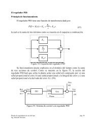
Chapter 5: <strong>Design</strong> of Transitions for High-Speed Signals<br />
X-Ref Target - Figure 5-1<br />
Td<br />
C<br />
50Ω<br />
2Td<br />
Figure 5-1:<br />
TDR Signature of Shunt Capacitance<br />
<strong>UG393</strong>_c5_01_091809<br />
X-Ref Target - Figure 5-2<br />
50Ω<br />
Figure 5-2:<br />
TDR Signature of Series Inductance<br />
<strong>UG393</strong>_c5_02_091809<br />
The magnitude of this excess capacitance (C) or inductance (L) can also be extracted from<br />
the TDR waveform by integrating the normalized area of the transition’s TDR response.<br />
The respective equations for capacitance and inductance are:<br />
t2<br />
2 V tdr () t – V step<br />
C = – -----<br />
Z 0<br />
∫<br />
------------------------------------ dt<br />
V<br />
t1 step<br />
t2 V tdr () t – V step<br />
L = 2Z 0 ∫<br />
------------------------------------ dt<br />
V<br />
t1 step<br />
Figure 5-3 shows the integration of the normalized TDR area.<br />
Equation 5-1<br />
Equation 5-2<br />
X-Ref Target - Figure 5-3<br />
t 1<br />
t 2<br />
Shaded area goes into the<br />
integral for Equation 13-2<br />
<strong>UG393</strong>_c5_03_091809<br />
Figure 5-3:<br />
Integration of Normalized TDR Area<br />
48 www.xilinx.com <strong>Spartan</strong>-6 <strong>FPGA</strong> <strong>PCB</strong> <strong>Design</strong> and Pin Planning<br />
<strong>UG393</strong> (v1.1) April 29, 2010