TSV technology for large die Cu/low K chip packaging
TSV technology for large die Cu/low K chip packaging
TSV technology for large die Cu/low K chip packaging

Create successful ePaper yourself
Turn your PDF publications into a flip-book with our unique Google optimized e-Paper software.
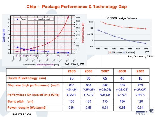
Chip – Package Per<strong>for</strong>mance & Technology Gap<br />
IC / PCB design features<br />
Ref; Gottward, EIPC<br />
Ref: J Wolf, IZM<br />
2005 2006 2007 2008 2009<br />
<strong>Cu</strong> <strong>low</strong> K <strong>technology</strong> (nm) 90 65 65 45 45<br />
Chip size (high per<strong>for</strong>mance) (mm 2 ) 600<br />
630<br />
662<br />
695<br />
729<br />
(~24x24)<br />
(~25x25)<br />
(~26x26)<br />
(~26x26)<br />
(~27x27)<br />
Per<strong>for</strong>mance On-<strong>chip</strong>/off-<strong>chip</strong> (GHz) 5.2/3.1 5.7/3.9 6.8/4.9 8.1/6.1 9.8/7.6<br />
Bump pitch (um) 150 130 130 130 120<br />
Power density (Watt/mm2) 0.54 0.58 0.61 0.64 0.64<br />
Ref: ITRS 2006