TSV technology for large die Cu/low K chip packaging
TSV technology for large die Cu/low K chip packaging
TSV technology for large die Cu/low K chip packaging

You also want an ePaper? Increase the reach of your titles
YUMPU automatically turns print PDFs into web optimized ePapers that Google loves.
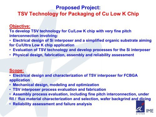
Proposed Project:<br />
<strong>TSV</strong> Technology <strong>for</strong> Packaging of <strong>Cu</strong> Low K Chip<br />
Objective:<br />
To develop <strong>TSV</strong> <strong>technology</strong> <strong>for</strong> <strong>Cu</strong>/Low K <strong>chip</strong> with very fine pitch<br />
interconnection involving:<br />
• Electrical design of Si interposer and a simplified organic substrate aiming<br />
<strong>for</strong> <strong>Cu</strong>/Ultra Low K <strong>chip</strong> application<br />
• Evaluation of <strong>TSV</strong> <strong>technology</strong> and develop processes <strong>for</strong> the Si interposer<br />
• Physical design, fabrication, assembly and reliability assessment<br />
Scope:<br />
• Electrical design and characterization of <strong>TSV</strong> interposer <strong>for</strong> FCBGA<br />
application<br />
• Mechanical design, modeling and optimization<br />
• <strong>TSV</strong> interposer process evaluation and fabrication<br />
• Assembly process evaluation, including fine pitch interconnection, under<br />
fill / flux material characterization and selection, wafer backgrind and dicing<br />
• Reliability assessment and failure analysis