Rahul Dewan - Jacobs University
Rahul Dewan - Jacobs University
Rahul Dewan - Jacobs University

You also want an ePaper? Increase the reach of your titles
YUMPU automatically turns print PDFs into web optimized ePapers that Google loves.
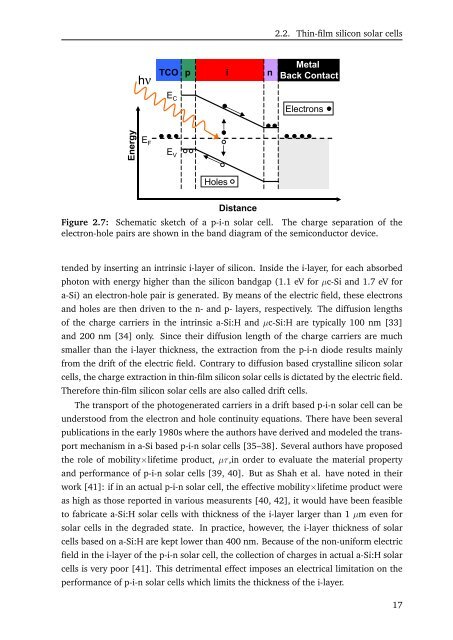
2.2. Thin-film silicon solar cells<br />
hν<br />
TCO p i n<br />
E C<br />
Metal<br />
Back Contact<br />
Electrons<br />
Energy<br />
E F<br />
E V<br />
Holes<br />
Distance<br />
Figure 2.7: Schematic sketch of a p-i-n solar cell. The charge separation of the<br />
electron-hole pairs are shown in the band diagram of the semiconductor device.<br />
tended by inserting an intrinsic i-layer of silicon. Inside the i-layer, for each absorbed<br />
photon with energy higher than the silicon bandgap (1.1 eV for µc-Si and 1.7 eV for<br />
a-Si) an electron-hole pair is generated. By means of the electric field, these electrons<br />
and holes are then driven to the n- and p- layers, respectively. The diffusion lengths<br />
of the charge carriers in the intrinsic a-Si:H and µc-Si:H are typically 100 nm [33]<br />
and 200 nm [34] only. Since their diffusion length of the charge carriers are much<br />
smaller than the i-layer thickness, the extraction from the p-i-n diode results mainly<br />
from the drift of the electric field. Contrary to diffusion based crystalline silicon solar<br />
cells, the charge extraction in thin-film silicon solar cells is dictated by the electric field.<br />
Therefore thin-film silicon solar cells are also called drift cells.<br />
The transport of the photogenerated carriers in a drift based p-i-n solar cell can be<br />
understood from the electron and hole continuity equations. There have been several<br />
publications in the early 1980s where the authors have derived and modeled the transport<br />
mechanism in a-Si based p-i-n solar cells [35–38]. Several authors have proposed<br />
the role of mobility×lifetime product, µτ,in order to evaluate the material property<br />
and performance of p-i-n solar cells [39, 40]. But as Shah et al. have noted in their<br />
work [41]: if in an actual p-i-n solar cell, the effective mobility×lifetime product were<br />
as high as those reported in various measurents [40, 42], it would have been feasible<br />
to fabricate a-Si:H solar cells with thickness of the i-layer larger than 1 µm even for<br />
solar cells in the degraded state. In practice, however, the i-layer thickness of solar<br />
cells based on a-Si:H are kept lower than 400 nm. Because of the non-uniform electric<br />
field in the i-layer of the p-i-n solar cell, the collection of charges in actual a-Si:H solar<br />
cells is very poor [41]. This detrimental effect imposes an electrical limitation on the<br />
performance of p-i-n solar cells which limits the thickness of the i-layer.<br />
17