Rahul Dewan - Jacobs University
Rahul Dewan - Jacobs University
Rahul Dewan - Jacobs University

Create successful ePaper yourself
Turn your PDF publications into a flip-book with our unique Google optimized e-Paper software.
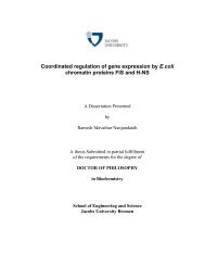
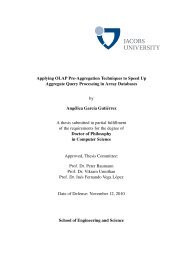
4. µC-SI SOLAR CELLS WITH INTEGRATED LAMELLAR GRATINGS<br />
Incoming<br />
Light<br />
Glass<br />
Glass<br />
Glass<br />
Transparent<br />
Conductive Oxide<br />
ZnO: Al<br />
ZnO: Al<br />
Microcrystalline<br />
Silicon Diode<br />
µc-Si<br />
Profile<br />
Height<br />
µc-Si<br />
Metal<br />
Back Contact<br />
Metal<br />
Back Contact<br />
Metal<br />
Back Contact<br />
Period<br />
(a) (b) (c)<br />
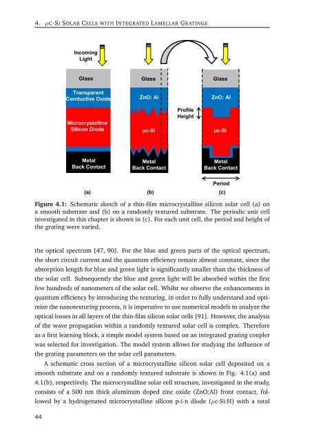
Figure 4.1: Schematic sketch of a thin-film microcrystalline silicon solar cell (a) on<br />
a smooth substrate and (b) on a randomly textured substrate. The periodic unit cell<br />
investigated in this chapter is shown in (c). For each unit cell, the period and height of<br />
the grating were varied.<br />
the optical spectrum [47, 90]. For the blue and green parts of the optical spectrum,<br />
the short circuit current and the quantum efficiency remain almost constant, since the<br />
absorption length for blue and green light is significantly smaller than the thickness of<br />
the solar cell. Subsequently the blue and green light will be absorbed within the first<br />
few hundreds of nanometers of the solar cell. Whilst we observe the enhancements in<br />
quantum efficiency by introducing the texturing, in order to fully understand and optimize<br />
the nanotexturing process, it is imperative to use numerical models to analyze the<br />
optical losses in all layers of the thin-film silicon solar cells [91]. However, the analysis<br />
of the wave propagation within a randomly textured solar cell is complex. Therefore<br />
as a first learning block, a simple model system based on an integrated grating coupler<br />
was selected for investigation. The model system allows for studying the influence of<br />
the grating parameters on the solar cell parameters.<br />
A schematic cross section of a microcrystalline silicon solar cell deposited on a<br />
smooth substrate and on a randomly textured substrate is shown in Fig. 4.1(a) and<br />
4.1(b), respectively. The microcrystalline solar cell structure, investigated in the study,<br />
consists of a 500 nm thick aluminum doped zinc oxide (ZnO:Al) front contact, followed<br />
by a hydrogenated microcrystalline silicon p-i-n diode (µc-Si:H) with a total<br />
44