
You also want an ePaper? Increase the reach of your titles
YUMPU automatically turns print PDFs into web optimized ePapers that Google loves.
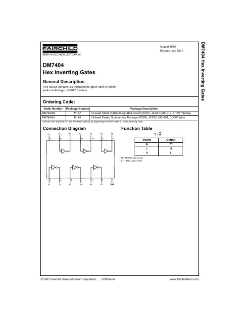
<strong>DM7404</strong><br />
<strong>Hex</strong> <strong>Inverting</strong> <strong>Gates</strong><br />
General Description<br />
This device contains six independent gates each of which<br />
performs the logic INVERT function.<br />
Ordering Code:<br />
August 1986<br />
Revised July 2001<br />
<strong>DM7404</strong> <strong>Hex</strong> <strong>Inverting</strong> <strong>Gates</strong><br />
Order Number Package Number Package Description<br />
<strong>DM7404</strong>M M14A 14-Lead Small Outline Integrated Circuit (SOIC), JEDEC MS-012, 0.150" Narrow<br />
<strong>DM7404</strong>N N14A 14-Lead Plastic Dual-In-Line Package (PDIP), JEDEC MS-001, 0.300" Wide<br />
Devices also available in Tape and Reel. Specify by appending the suffix letter “X” to the ordering code.<br />
Connection Diagram<br />
Function Table<br />
H = HIGH Logic Level<br />
L = LOW Logic Level<br />
Inputs<br />
A<br />
L<br />
H<br />
Y = A<br />
Output<br />
Y<br />
H<br />
L<br />
© 2001 Fairchild Semiconductor Corporation DS006494 www.fairchildsemi.com
<strong>DM7404</strong><br />
Absolute Maximum Ratings(Note 1)<br />
Supply Voltage<br />
7V<br />
Input Voltage 5.5V<br />
Operating Free Air Temperature Range 0°C to +70°C<br />
Storage Temperature Range<br />
−65°C to +150°C<br />
Note 1: The “Absolute Maximum Ratings” are those values beyond which<br />
the safety of the device cannot be guaranteed. The device should not be<br />
operated at these limits. The parametric values defined in the Electrical<br />
Characteristics tables are not guaranteed at the absolute maximum ratings.<br />
The “Recommended Operating Conditions” table will define the conditions<br />
for actual device operation.<br />
Recommended Operating Conditions<br />
Symbol Parameter Min Nom Max Units<br />
V CC Supply Voltage 4.75 5 5.25 V<br />
V IH HIGH Level Input Voltage 2 V<br />
V IL LOW Level Input Voltage 0.8 V<br />
I OH HIGH Level Output Current −0.4 mA<br />
I OL LOW Level Output Current 16 mA<br />
T A Free Air Operating Temperature 0 70 °C<br />
Electrical Characteristics<br />
over recommended operating free air temperature range (unless otherwise noted)<br />
Typ<br />
Symbol Parameter Conditions Min<br />
(Note 2)<br />
Max Units<br />
V I Input Clamp Voltage V CC = Min, I I = −12 mA −1.5 V<br />
V OH HIGH Level V CC = Min, I OH = Max<br />
Output Voltage<br />
V IL = Max<br />
2.4 3.4 V<br />
V OL LOW Level V CC = Min, I OL = Max<br />
Output Voltage<br />
V IH = Min<br />
0.2 0.4 V<br />
I I Input Current @ Max Input Voltage V CC = Max, V I = 5.5V 1 mA<br />
I IH HIGH Level Input Current V CC = Max, V I = 2.4V 40 µA<br />
I IL LOW Level Input Current V CC = Max, V I = 0.4V −1.6 mA<br />
I OS Short Circuit Output Current V CC = Max (Note 3) −18 −55 mA<br />
I CCH Supply Current with Outputs HIGH V CC = Max 6 12 mA<br />
I CCL Supply Current with Outputs LOW V CC = Max 18 33 mA<br />
Note 2: All typicals are at V CC = 5V, T A = 25°C.<br />
Note 3: Not more than one output should be shorted at a time.<br />
Switching Characteristics<br />
at V CC = 5V and T A = 25°C<br />
Symbol Parameter Conditions Min Max Units<br />
t PLH Propagation Delay Time C L = 15 pF<br />
LOW-to-HIGH Level Output<br />
R L = 400Ω<br />
22 ns<br />
t PHL Propagation Delay Time<br />
HIGH-to-LOW Level Output<br />
15 ns<br />
www.fairchildsemi.com 2
Physical Dimensions inches (millimeters) unless otherwise noted<br />
<strong>DM7404</strong><br />
14-Lead Small Outline Integrated Circuit (SOIC), JEDEC MS-012, 0.150" Narrow<br />
Package Number M14A<br />
3 www.fairchildsemi.com
<strong>DM7404</strong> <strong>Hex</strong> <strong>Inverting</strong> <strong>Gates</strong><br />
Physical Dimensions inches (millimeters) unless otherwise noted (Continued)<br />
14-Lead Plastic Dual-In-Line Package (PDIP), JEDEC MS-001, 0.300" Wide<br />
Package Number N14A<br />
Fairchild does not assume any responsibility for use of any circuitry described, no circuit patent licenses are implied and<br />
Fairchild reserves the right at any time without notice to change said circuitry and specifications.<br />
LIFE SUPPORT POLICY<br />
FAIRCHILD’S PRODUCTS ARE NOT AUTHORIZED FOR USE AS CRITICAL COMPONENTS IN LIFE SUPPORT<br />
DEVICES OR SYSTEMS WITHOUT THE EXPRESS WRITTEN APPROVAL OF THE PRESIDENT OF FAIRCHILD<br />
SEMICONDUCTOR CORPORATION. As used herein:<br />
1. Life support devices or systems are devices or systems<br />
which, (a) are intended for surgical implant into the<br />
body, or (b) support or sustain life, and (c) whose failure<br />
to perform when properly used in accordance with<br />
instructions for use provided in the labeling, can be reasonably<br />
expected to result in a significant injury to the<br />
user.<br />
www.fairchildsemi.com 4<br />
2. A critical component in any component of a life support<br />
device or system whose failure to perform can be reasonably<br />
expected to cause the failure of the life support<br />
device or system, or to affect its safety or effectiveness.<br />
www.fairchildsemi.com