Rated Power and VSWR Improvement of Termination Resistor with ...
Rated Power and VSWR Improvement of Termination Resistor with ...
Rated Power and VSWR Improvement of Termination Resistor with ...

You also want an ePaper? Increase the reach of your titles
YUMPU automatically turns print PDFs into web optimized ePapers that Google loves.
March 28-31, 2011 CARTS USA 2011 Jacksonville, FL<br />
<strong>Rated</strong> <strong>Power</strong> <strong>and</strong> <strong>VSWR</strong> <strong>Improvement</strong> <strong>of</strong> <strong>Termination</strong><br />
<strong>Resistor</strong> <strong>with</strong> Innovative Design <strong>and</strong> Integrated Matching<br />
Network<br />
Abstract<br />
A. Rahman, F. Olinger, <strong>and</strong> M. Howieson<br />
Thin Film Technology Corporation<br />
1980 Commerce Drive,<br />
North Mankato, MN, 56003, USA<br />
Phone: 507-625-8445, Fax: 507-625-9175, email: arahman@thin-film.com<br />
Matching RF <strong>and</strong> Microwave signals to components <strong>with</strong>in a circuit has become more<br />
challenging for circuit designer as operating frequency <strong>and</strong> power h<strong>and</strong>ling requirement<br />
increase. <strong>Termination</strong> resistors <strong>with</strong> excellent power h<strong>and</strong>ling capability <strong>with</strong> superior<br />
voltage st<strong>and</strong>ing wave ratio (<strong>VSWR</strong>) characteristics are needed for microwave circuit<br />
components in various wireless <strong>and</strong> telecommunication application. In this work, we<br />
extensively studied to improve the power h<strong>and</strong>ling capability <strong>and</strong> <strong>VSWR</strong> <strong>of</strong> termination<br />
resistor while maintaining the smaller size. We optimized the energy transmission <strong>with</strong>in the<br />
component <strong>and</strong> significantly improved the efficiency <strong>of</strong> energy transfer between the<br />
transmission lines <strong>and</strong> the terminations. We discussed techniques <strong>of</strong> improving power<br />
h<strong>and</strong>ling capability <strong>and</strong> reduction <strong>of</strong> thermal fatigue to the component’s structure. By using<br />
innovative techniques <strong>of</strong> heat transfer we appreciably increased power h<strong>and</strong>ling capability<br />
while keeping the product size as minimum. We improved the package technology <strong>and</strong><br />
reduced the chance <strong>of</strong> solder cracking due to thermal fatigue. We constructed matching<br />
network using integrated microstrip line at the beginning <strong>of</strong> the resistor material. We<br />
optimized impedance matching by varying length, width <strong>and</strong> pattern <strong>of</strong> transmission line as<br />
well as using defective ground structure (DGS) technique. We minimized the detrimental<br />
influence <strong>of</strong> component footprint <strong>and</strong> resistor material characteristics effect on signal<br />
reflection.<br />
Considering the necessary microwave parameters <strong>and</strong> required thermal performance, we<br />
designed <strong>and</strong> manufactured Pb free high power termination resistor. Several sizes <strong>of</strong> resistor<br />
are manufactured <strong>with</strong> rated power <strong>of</strong> 20 Watt, <strong>and</strong> 100 Watt which provides excellent<br />
<strong>VSWR</strong> characteristics for frequency up to 4 GHz. <strong>Resistor</strong>s are manufactured for 50 ohm<br />
impedance; however, methods mentioned in the study are applicable to any impedance.<br />
Introduction:
The wireless telecommunication, broadcast <strong>and</strong> radar industries rely on high power<br />
transmission <strong>of</strong> the radio waves to reach subscribers or measure the environment. Ever<br />
growing multimedia data communication constantly increases data traffic to the systems. As<br />
the wireless revolution extends, component requirement in higher frequency, elevated<br />
operating power, smaller in size, <strong>and</strong> improved performance dem<strong>and</strong>s on resistive devices<br />
grow even more stringent. Several research works have been done on increasing power<br />
h<strong>and</strong>ling capability in smaller size resistors. Other work was done on 50 Ω microwave<br />
termination resistors for up to certain frequency. Simulant high power resistor development<br />
technique was discussed in [1]. Based on proven ceramic resistor technology, a new type <strong>of</strong><br />
power resistor has been developed to <strong>of</strong>fer significant advantages over conventional wire<br />
wound <strong>and</strong> thick/thin film devices [2]. <strong>Power</strong>-dividing-based microwave power thin film<br />
resistor (MPTFR) that exhibits high operating frequency <strong>and</strong> high power load was discussed<br />
in [3]. Thick film <strong>and</strong> wirewound resistors were studied for high temperature storage <strong>and</strong><br />
thermal cycle [4]. Ceramic component <strong>of</strong> high energy resistors ware studied in [5].<br />
Microwave transmission line <strong>with</strong> dielectric <strong>and</strong> ground plane <strong>and</strong> its importance was argued<br />
in [6].<br />
In this work, we studied how to improve the microwave termination resistor’s power<br />
h<strong>and</strong>ling capability while keeping the size smaller. One <strong>of</strong> the eminent reasons <strong>of</strong> power<br />
resistors failure is not being able to keep surface temperature below the level <strong>of</strong> component<br />
failure mode. We analyzed how to remove the heat as the component surface temperature<br />
increases. We explored techniques on efficiently heat dissipation through the resistors. Then<br />
we applied this heat removal technique for microwave termination resistors. For higher<br />
frequency compatibility, we used integrated impedance matching network on the resistor<br />
surface to achieve excellent return loss characteristics. We used High Z Low Z transmission<br />
line method to realize the impedance matching network. Based on the simulation results we<br />
fabricated the chip power resistors. We provided return loss characteristics frequency <strong>of</strong><br />
response results <strong>and</strong> thermal pr<strong>of</strong>ile <strong>of</strong> the fabricated termination power resistor. Thermal<br />
pr<strong>of</strong>ile demonstrates the true power h<strong>and</strong>ling capability <strong>of</strong> the resistor.<br />
Improving rated power efficiency in chip resistor:<br />
The biggest challenge to improve power efficiency in chip resistor is heat removal. As the<br />
power gets increased, the product gets extremely hot <strong>and</strong> starts to degrade its performance.<br />
Excessive generated heat can change the resistor value during hot temperature. If the power<br />
resistor is extremely hot for a longer period <strong>of</strong> time, the heat can cause irreversible change in<br />
the resistance. <strong>Resistor</strong> eventually starts entering in the failure mode <strong>and</strong> finally quits<br />
performing. We worked on several different ways to efficiently reduce the heat. Since the<br />
product size is exceptionally small to remove excessive generated heat, we improved several<br />
different parameters <strong>of</strong> the product to remove heat. We worked on mainly three key areas to<br />
reduce heat from the product surface. We improved the product to distribute the uniformly to<br />
entire resistor <strong>and</strong> improve current density. Then we lowered the thermal resistive interface<br />
between the chip <strong>and</strong> printed circuit board. Finally we improved the rate <strong>of</strong> heat transfer from<br />
the resistor to the circuit board.
Improve heat dissipation:<br />
The dominant form <strong>of</strong> heat removal from a chip power resistor is by conduction through the<br />
circuit board from which heat is removed from the larger area <strong>of</strong> the board, ultimately by<br />
convection. We significantly enlarged the resistive material area in the chip to uniformly<br />
distribute the heat in all part <strong>of</strong> the resistor. As a result, we eliminated one single point <strong>of</strong><br />
heat transfer. Using distinctive thin film sputtering process, we maximized the resistive<br />
portion <strong>of</strong> the chip, therefore resistive material is distributed uniformly throughout the<br />
product. Consequently, heat is removed throughout the product instead on one single point.<br />
Accordingly, no single point gets too hot to make the part damaged. Hence excessive power<br />
is dissipated in a smaller size chip <strong>with</strong>out increasing the peak surface temperature<br />
Bigger resistive area <strong>of</strong> the product not only helps <strong>with</strong> uniformly distribute the heat; it also<br />
improves the current density. Just as overheating a resistor can cause irreversible changes in<br />
resistance, exceeding the resistive elements maximum current density can as well – even if<br />
the heat is sufficiently conducted away. The maximum current density refers to the<br />
maximum tolerated current per unit <strong>of</strong> cross-sectional area perpendicular to the current <strong>of</strong> the<br />
conducting resistive element before subjected to mass transport effects (i.e. electromigration).<br />
Electro-migration results in the drift <strong>of</strong> atoms in the conducting material. The<br />
drift <strong>of</strong> atoms is due to the continuous momentum transfer from conducting electrons.<br />
Electrons have very little mass, so it takes a lot <strong>of</strong> them at once to carry enough energy to<br />
make an atom from the structure <strong>of</strong> the resistive element drift. This effectively reduces at<br />
some point the cross-sectional area <strong>of</strong> the conducting resistive element. As this process <strong>of</strong><br />
electro-migration continues, the probability <strong>of</strong> additional electro-migration becomes greater<br />
<strong>and</strong> greater. For instance, applying a current source in excess <strong>of</strong> the maximum current<br />
density <strong>of</strong> a resistor would lead to eventual resistive runaway.<br />
The material properties <strong>of</strong> the resistive element determine the current density limit <strong>and</strong> play a<br />
major role in the resulting absolute maximum power <strong>and</strong> pulse power ratings for a given<br />
design <strong>and</strong> level <strong>of</strong> reliability. We used Nickel Chromium as resistive material. Nickel<br />
Chromium has very high current density limits, which make them very suitable for surface<br />
mount power resistor applications. In addition, since Nickel Chromium is deposited directly<br />
onto the thermally conductive chip carrier <strong>with</strong> which they have an intimate interface, there<br />
is virtually zero thermal resistance between them.<br />
Improve thermal resistivity:<br />
After convection process, the most significant path to remove heat is the component<br />
footprint. Heat is generated in the resistor surface area then it travels through the footprint to<br />
the circuit board. By optimizing the heat transfer through the footprint can improve the<br />
power dissipation process. A lower thermal resistance interface will enable more efficient<br />
heat transfer from the component, enabling lower surface temperatures at greater power
levels by making good use <strong>of</strong> the relatively larger area <strong>of</strong> the circuit board to dissipate the<br />
heat.<br />
We explored the ways to improve heat transfer through the footprint. We established a low<br />
thermal resistance interface from the resistive element to the circuit board. We maximized<br />
the termination electrode’s size. Therefore heat has more ways to transfer from the surface to<br />
the circuit board. We also used high purity, high thermal conductivity chip carrier to further<br />
lower the thermal resistivity. We also investigated special design consideration, to ensure a<br />
balanced distribution <strong>of</strong> the generated heat.<br />
Improve heat transfer rate:<br />
We studied to improve the heat transfer rate through the component footprint. We realized<br />
that the faster the heat can transfer from the electrodes, the less time the heat has to keep the<br />
electrodes hot. If the heat cannot move faster through the electrodes <strong>and</strong> more heat is<br />
generating in the chip resistor, then the electrodes keep getting hotter. As the temperature<br />
rise, at some point the surface temperature could exceed the melting point <strong>of</strong> the mounting<br />
solder <strong>and</strong> potentially makes a crack in the solder joint. This phenomenon can potentially<br />
cause irreversible changes in resistance – as well as potential damage to the printed circuit<br />
board. We significantly improved the rate <strong>of</strong> heat transfer through the termination electrodes.<br />
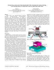
We showed the result <strong>of</strong> the heat transfer improvement in Figure 1.<br />
Fig 1 a. Conventional power resistor after 1000 cycle<br />
Fig 1 b. TFT power chip resistor after 1000 cycle
Fig 1 c. Conventional power resistor after 2000 cycle<br />
Fig 1 d. TFT power chip resistor after 2000 cycle<br />
Figure 1. <strong>Power</strong> chip resistors solder joint picture after applying high temperature expected<br />
to generate from dissipated power.<br />
Figure 1a <strong>and</strong> Figure1c represent conventional chip resistor where heat transfer rate is<br />
ordinary. It illustrates that excessive heat made the temperature rise more than the melting<br />
point <strong>of</strong> mounting solder <strong>and</strong> made a crack in the resistor joint. As a result the product went<br />
into failure more. Figure 1b <strong>and</strong> Figure 1d represents our new improved chip resistor, where<br />
heat transfer rate is optimized. This figure demonstrates that for exact same heat, generated<br />
from applied power, there is no change in the solder joint. As a no result, no damage is done<br />
in the chip resistor. For this test, we used thermal shock cycles. Test condition was -55˚<br />
temperature applied for 30 min , followed by room temperature applied for 3min followed by<br />
+155°C applied for 30min, followed by room temperature applied for 3min, repeating to<br />
1000 cycles <strong>and</strong> 2000 cycles on FR4 0.6mm thickness PC board.<br />
Thermal pr<strong>of</strong>ile comparison:<br />
After making the several changes in heat removal process we fabricated the chip power<br />
resistor. Then we compared the temperature differences between conventional chip resistor<br />
<strong>and</strong> our new chip power resistor. Figure 2 illustrates the thermal pr<strong>of</strong>ile <strong>of</strong> the comparison<br />
between two chip power resistors. In the figure, the thermal pr<strong>of</strong>iles shows the surface<br />
temperature differences between a conventional chip power resistor <strong>and</strong> our improved chip<br />
power resistor, at thermal equilibrium. The horizontal line across the thermal images titled<br />
REGION (extending across electrodes) is the position for the pr<strong>of</strong>iles shown in Figure 2.<br />
The chip power resistors compared are identical sizes (2525, 6.3 x 6.3 mm) <strong>and</strong> mounted to
identical PCB’s (1 x 3 inch FR-4) <strong>with</strong> the same amount <strong>of</strong> power applied in a static<br />
environment (no air flow). Each was coated <strong>with</strong> a flat black paint to eliminate any<br />
emissivity differences that might have biased the infrared images.<br />
Figure 2a. Thermal pr<strong>of</strong>ile for conventional<br />
type chip power resistor<br />
Figure 2b. Thermal pr<strong>of</strong>ile for improved<br />
chip power resistor<br />
Fig 2a illustrates the presence <strong>of</strong> the single point in the chip surface. For the given power,<br />
temperature rises from all sides <strong>of</strong> the part to the middle <strong>of</strong> the part. In the middle, peak<br />
surface temperature rose as much as 180˚ C. Fig 2b illustrates the surface temperature for the<br />
same given power. Here temperature is distributed uniformly to the whole chip. Surface<br />
temperature never rises more than 137˚ C. In the figures, green color represents the printed<br />
circuit board temperature. In Figure 2a, PCB temperature is around 80˚ C; while in figure 2b,<br />
PCB temperature is around 100˚ C. The ratio <strong>of</strong> the differences between electrode <strong>and</strong> PCB<br />
temperatures (from the thermal pr<strong>of</strong>iles shown in Figure 2 demonstrates how much more<br />
efficiently the new power resistor removes heat from the resistive element to the PCB. The<br />
far more uniform surface temperature <strong>of</strong> the new power resistor is a further testament <strong>of</strong> this.
The sample PCB used for this test are far from thermally optimized, as can be seen from how<br />
cool the board temperature is around the parts compared to the surface temperature <strong>of</strong> the<br />
electrodes, for the purpose <strong>of</strong> more clearly illustrating the differences. For thermally<br />
optimized PCB, the improved power efficient chip resistor are designed to tolerate current<br />
densities that equate to as much as 70W – that is if the PCB can sufficiently dissipate the heat<br />
<strong>with</strong> a reasonable surface temperature.<br />
Improving Voltage St<strong>and</strong>ing Wave Ratio (<strong>VSWR</strong>) in chip resistor:<br />
One <strong>of</strong> the most important parameter <strong>of</strong> the 50 Ω termination resistor is impedance match<br />
<strong>with</strong> the RF/Mirowave signal. If the termination resistor posses an RF impedance, which is<br />
not 50 Ω, significant energy reflects back into circuit by the unmatched termination. This<br />
signal reflection elevates the voltage st<strong>and</strong>ing wave ratio (<strong>VSWR</strong>) in the circuit. This<br />
phenomenon degrades the circuit efficiency. RF engineers require that the <strong>VSWR</strong> be as close<br />
to unity as possible. <strong>VSWR</strong> is an indicator <strong>of</strong> how well the parts absorb energy <strong>and</strong> not<br />
reflect it in the opposite direction. Unity <strong>VSWR</strong> indicates complete impedance match<br />
between transmitted <strong>and</strong> reflected signal. As the operating frequency gets increased<br />
termination resistor must have good <strong>VSWR</strong> for ever higher frequency. Current system design<br />
environment requires termination resistor to have excellent <strong>VSWR</strong> specification up to 3.0<br />
GHz.<br />
We have used several innovative techniques to improve the impedance match for the<br />
termination resistor. First we developed the power resistor for the termination resistor. We<br />
used above discussed technique to make high rated 50 Ω power resistor. Then we designed<br />
integrated matching network. We used High Z <strong>and</strong> Low Z transmission line method for<br />
impedance match. Even though serpentine <strong>and</strong> L-shaped matching network can provide good<br />
matching result, however, it takes more space in the resistor surface. By using High Z Low Z<br />
transmission line method, we kept the chip size significantly smaller, which lets maximize<br />
the resistor surface area. Higher resistor surface area helped us to uniformly distribute the<br />
heat so the product can h<strong>and</strong>le higher power dissipation.
Figure 3a. Design Layout <strong>of</strong> the termination power<br />
Figure 3b. Return loss simulation result <strong>of</strong> the<br />
resistor designed termination resistor<br />
Since we extended the resistor surface area, it adds up significant capacitor value, which<br />
degrades the <strong>VSWR</strong> performance. Due to the additional capacitance we changed the<br />
integrated matching network. We utilize the influence <strong>of</strong> excessive capacitance to improve<br />
the <strong>VSWR</strong>. We also use Degenerative Ground Structure (DGS) to further improve the<br />
<strong>VSWR</strong> characteristics. In DGS, we intentionally change the ground path to improve the<br />
<strong>VSWR</strong> characteristics.<br />
Figure 3a <strong>and</strong> 3b shows the design <strong>and</strong> simulated result <strong>of</strong> 20 W RF power chip resistor<br />
respectively. Figure 3a demonstrates that the resistor is maximally extended for optimized<br />
power dissipation <strong>and</strong> usage <strong>of</strong> High Z low Z transmission line method for impedance<br />
matching network. Figure 3b shows the return loss plot <strong>of</strong> the designed termination resistor.
Simulation plot illustrates that return loss value is -16.5 dB at 4.0 GHz. From <strong>VSWR</strong> <strong>and</strong><br />
Return Loss calculation, one can find that <strong>VSWR</strong> is 1.35:1 at 4.0 GHz frequency.<br />
Component fabrication <strong>and</strong> measured results:<br />
Based on the excellent theoretical <strong>and</strong> simulation work to design 50 Ω RF termination<br />
resistor, we manufactured termination resistor <strong>with</strong> 20W <strong>and</strong> 100W power h<strong>and</strong>ling<br />
capability. We used high purity Aluminum Nitrate (ALN) as substrate due to its higher<br />
thermal conductivity. Its thermal conductivity is 170 – 180 W/meter ˚C. For resistive element<br />
we used Nickel Chromium as thin film material. Epoxy-resin was used as overcoat. For chip<br />
termination, we used pre-tinned (Sn100, Matte) material over Nickel (Ni) barrier.<br />
Fig 5a. 20 Watt power resistor in RFevaluation board<br />
Fig 5b. 100 Watt power resistor in RF evaluation board<br />
For RF measurement purpose, the manufactured resistor was mounted in Rogers 4350B 10<br />
mil thick printed circuit board. PCB along <strong>with</strong> the component was then placed in TFT’s<br />
evaluation board. Figure 5a <strong>and</strong> 5b illustrate 20 Watt resistor <strong>and</strong> 100 Watt resistor mounted<br />
in measurement module. As the resistor performance we achieved tolerance <strong>of</strong> less +/- 1%.<br />
We realized TCR level <strong>of</strong> +/- 25 parts per million (PPM) for these chip power resistors.
Figure 6a. Return loss characteristics <strong>of</strong> 20 Watt power<br />
resistor in RF evaluation board<br />
Figure 6b. Return loss characteristics <strong>of</strong> 100 Watt power<br />
resistor in RF evaluation board<br />
Figure 6a <strong>and</strong> figure 6b illustrate Return Loss characteristics <strong>of</strong> frequency response <strong>of</strong> 20<br />
Watt <strong>and</strong> 100 Watt power resistor respectively. Return loss plot <strong>of</strong> frequency response<br />
illustrate that return loss value is around -20 dB for both the parts at 3.0 GHz. From <strong>VSWR</strong><br />
<strong>and</strong> Return Loss calculation, one can find that <strong>VSWR</strong> is 1.16:1 at 3.0 GHz frequency. At 4.0<br />
GHz frequency, <strong>VSWR</strong> is 1.43:1 for 20 Watt power termination resistor <strong>and</strong> 1.95:1 for 100<br />
Watt power termination resistor respectively.<br />
Then we measured the true power h<strong>and</strong>ling capability <strong>of</strong> both resistors. We applied power<br />
<strong>and</strong> observed the surface temperature <strong>of</strong> the resistors. First we applied the rated power for
oth resistors. Then we increased the power to measure how much power is needed for the<br />
peak surface temperature to reach 200˚C.<br />
Figure 7. . Thermal pr<strong>of</strong>ile <strong>of</strong> the 20 Watt <strong>and</strong> 100Watt chip power resistor.<br />
Figure 7 illustrate the thermal pr<strong>of</strong>ile <strong>of</strong> the peak surface temperature <strong>of</strong> 20 Watt <strong>and</strong> 100<br />
Watt new chip power resistor. From the figure, we can observe that for 20 Watt power<br />
resistor, at 20 Watt applied power, maximum surface temperature is 101˚C. For 100 Watt<br />
power resistor, at 100 Watt applied power, maximum surface temperature is 124˚C. This is<br />
much lower temperature for the resistor to enter in failure mode. One can also observe that<br />
for 20W resistor, it requires 37 Watt power for the peak surface temperature to be 200˚C.<br />
Similarly for 100W resistor, it requires 150 Watt power for the peak surface temperature to<br />
be 200˚C. This figure confirms that these chip power resistor can h<strong>and</strong>le more than one times<br />
<strong>and</strong> half <strong>of</strong> the rated power.<br />
Conclusion:<br />
In this work, we studied termination resistors <strong>and</strong> importance <strong>of</strong> impedance matching<br />
network <strong>and</strong> heat removal process <strong>of</strong> termination power resistor design. We investigated<br />
several innovative ways to efficiently remove heat from the resistor surface, resulting<br />
minimizing peak surface temperature to a level that will not cause resistor to enter in failure<br />
mode. We removed the heat by uniformly distributed the heat around the chip surface area<br />
<strong>and</strong> improved the heat transfer rate through the footprint. We showed the enhancement <strong>of</strong><br />
heat removal technique <strong>with</strong> surface temperature thermal pr<strong>of</strong>ile. Then we investigated<br />
impedance matching network technique <strong>and</strong> implemented High Z Low Z transmission line<br />
technique to successfully match impedance up to 4.0 GHz operating frequency. Simulation<br />
result shows excellent return loss characteristics <strong>of</strong> the power resistors. Then we<br />
manufactured 20 Watt <strong>and</strong> 100 Watt RF termination power resistor. We measured the
frequency response <strong>of</strong> the fabricated component. Return loss plots <strong>of</strong> the measured results<br />
proved exceptional <strong>VSWR</strong> characteristics <strong>of</strong> both power resistors. Then we tested the parts<br />
for rated power. We applied various power <strong>and</strong> tested for highest peak surface temperature<br />
rise. We provided thermal pr<strong>of</strong>ile plots <strong>of</strong> both 20 Watt <strong>and</strong> 100 Watt resistors. Thermal<br />
pr<strong>of</strong>ile demonstrates the outst<strong>and</strong>ing power h<strong>and</strong>ling capability <strong>of</strong> both RF termination<br />
power resistors.<br />
References:<br />
[1] H. Wang, H. Shao, Z. Li, B. Liang, <strong>and</strong> F. Lin, “Development <strong>of</strong> simulant high power<br />
resistor,” Precision Electromagnetic Measurement Digest, CPEM 2008, pp. 404, June.<br />
2008.<br />
[2] E. Smart, “A low pr<strong>of</strong>ile power resistor,” IEE Colloquium on Pulsed <strong>Power</strong> 97, pp. 26,<br />
Mar. 1997.<br />
[3] H.C. Jiang, X. Si, W. L. Zhang, C. J. Wang, B. Peng, <strong>and</strong> Y. R. Li “Microwave power<br />
thin film resistors for high frequency <strong>and</strong> high power load applications,” Applied<br />
Physics Letters., vol. 97,no. 17, pp. 13750, Oct. 2010.<br />
[4] J.E. Naefe, R.W. Johnson, <strong>and</strong> R.R. Grzybowski, “High-temperature storage <strong>and</strong> thermal<br />
cycling studies <strong>of</strong> thick film <strong>and</strong> wirewound resistors” IEEE trans. On Components <strong>and</strong><br />
Packaging Technologies, vol. 25,no. 1, pp. 45, Mar. 2002.<br />
[5] W.D. Glodzik, D.J. II Yanko, <strong>and</strong> K. Chia, “Advanced ceramic composite for high<br />
energy resistors; characterization <strong>of</strong> electrical <strong>and</strong> physical properties,” IEEE Tenth<br />
International Pulsed <strong>Power</strong> Conference., vol. 2, pp. 1422, Jul. 1995.<br />
[6] E. C. Smith, <strong>and</strong> R.S. Chang, “Microstrip transmission line <strong>with</strong> finite-width dielectric<br />
<strong>and</strong> ground plane,” IEEE transaction on Microwave Theory <strong>and</strong> Techniques, vol. MTT-<br />
33, no. 9, pp. 835-839, Sep. 1985.<br />
[7] J.S. Fisher, <strong>and</strong> P.M. Hall, “<strong>Termination</strong> material for thin film resistors,” Proceedings <strong>of</strong><br />
the IEEE, vol. 59, no. 10, pp. 1418, Oct. 1971.<br />
[8] S. Chen, P. Sun, X. Wei, Z. Cheng, <strong>and</strong> J. Liu, “Studies <strong>of</strong> solder joint reliability under<br />
mechanical bending test on FR-4 PCBs <strong>with</strong> Sn-1.0 Ag-0.5 Cu solder paste,”<br />
International Symposium on High Density packaging <strong>and</strong> Microsystem Integration<br />
(HDP 2007), pp. 1, June. 2007.