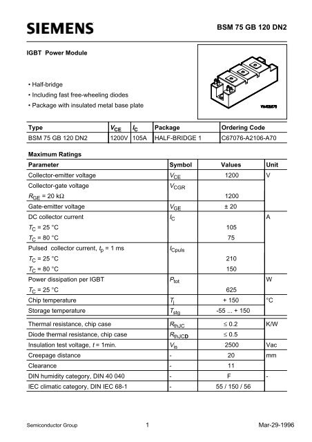
BSM 75 GB 120 DN2 - Datasheet Catalog
BSM 75 GB 120 DN2 - Datasheet Catalog
BSM 75 GB 120 DN2 - Datasheet Catalog

You also want an ePaper? Increase the reach of your titles
YUMPU automatically turns print PDFs into web optimized ePapers that Google loves.
<strong>BSM</strong> <strong>75</strong> <strong>GB</strong> <strong>120</strong> <strong>DN2</strong><br />
I<strong>GB</strong>T Power Module<br />
• Half-bridge<br />
• Including fast free-wheeling diodes<br />
• Package with insulated metal base plate<br />
Type V CE I C Package Ordering Code<br />
<strong>BSM</strong> <strong>75</strong> <strong>GB</strong> <strong>120</strong> <strong>DN2</strong> <strong>120</strong>0V 105A HALF-BRIDGE 1 C67076-A2106-A70<br />
Maximum Ratings<br />
Parameter Symbol Values Unit<br />
Collector-emitter voltage V CE <strong>120</strong>0 V<br />
Collector-gate voltage<br />
R GE = 20 kΩ<br />
V CGR<br />
<strong>120</strong>0<br />
Gate-emitter voltage V GE ± 20<br />
DC collector current<br />
T C = 25 °C<br />
T C = 80 °C<br />
Pulsed collector current, t p = 1 ms<br />
T C = 25 °C<br />
T C = 80 °C<br />
Power dissipation per I<strong>GB</strong>T<br />
T C = 25 °C<br />
I C<br />
105<br />
<strong>75</strong><br />
I Cpuls<br />
210<br />
150<br />
P tot<br />
625<br />
Chip temperature T j + 150 °C<br />
Storage temperature T stg -55 ... + 150<br />
Thermal resistance, chip case R thJC ≤ 0.2 K/W<br />
Diode thermal resistance, chip case R thJCD ≤ 0.5<br />
Insulation test voltage, t = 1min. V is 2500 Vac<br />
Creepage distance - 20 mm<br />
Clearance - 11<br />
DIN humidity category, DIN 40 040 - F -<br />
IEC climatic category, DIN IEC 68-1 - 55 / 150 / 56<br />
A<br />
W<br />
Semiconductor Group 1 Mar-29-1996
<strong>BSM</strong> <strong>75</strong> <strong>GB</strong> <strong>120</strong> <strong>DN2</strong><br />
Electrical Characteristics, at T j = 25 °C, unless otherwise specified<br />
Parameter Symbol Values Unit<br />
min. typ. max.<br />
Static Characteristics<br />
Gate threshold voltage<br />
V GE = V CE, I C = 3 mA<br />
Collector-emitter saturation voltage<br />
V GE = 15 V, I C = <strong>75</strong> A, T j = 25 °C<br />
V GE = 15 V, I C = <strong>75</strong> A, T j = 125 °C<br />
Zero gate voltage collector current<br />
V CE = <strong>120</strong>0 V, V GE = 0 V, T j = 25 °C<br />
V CE = <strong>120</strong>0 V, V GE = 0 V, T j = 125 °C<br />
Gate-emitter leakage current<br />
V GE = 20 V, V CE = 0 V<br />
AC Characteristics<br />
Transconductance<br />
V CE = 20 V, I C = <strong>75</strong> A<br />
Input capacitance<br />
V CE = 25 V, V GE = 0 V, f = 1 MHz<br />
Output capacitance<br />
V CE = 25 V, V GE = 0 V, f = 1 MHz<br />
Reverse transfer capacitance<br />
V CE = 25 V, V GE = 0 V, f = 1 MHz<br />
V GE(th)<br />
4.5 5.5 6.5<br />
V CE(sat)<br />
-<br />
-<br />
I CES<br />
-<br />
-<br />
2.5<br />
3.1<br />
1<br />
4.5<br />
3<br />
3.7<br />
1.5<br />
-<br />
I GES<br />
- - 320<br />
g fs<br />
31 - -<br />
C iss<br />
- 5.5 -<br />
C oss<br />
- 0.8 -<br />
C rss<br />
- 0.3 -<br />
V<br />
mA<br />
nA<br />
S<br />
nF<br />
Semiconductor Group 2 Mar-29-1996
<strong>BSM</strong> <strong>75</strong> <strong>GB</strong> <strong>120</strong> <strong>DN2</strong><br />
Electrical Characteristics, at T j = 25 °C, unless otherwise specified<br />
Parameter Symbol Values Unit<br />
min. typ. max.<br />
Switching Characteristics, Inductive Load at T j = 125 °C<br />
Turn-on delay time<br />
t d(on)<br />
V CC = 600 V, V GE = 15 V, I C = <strong>75</strong> A<br />
R Gon = 15 Ω<br />
- 30 60<br />
Rise time<br />
t r<br />
V CC = 600 V, V GE = 15 V, I C = <strong>75</strong> A<br />
R Gon = 15 Ω<br />
- 70 140<br />
Turn-off delay time<br />
t d(off)<br />
V CC = 600 V, V GE = -15 V, I C = <strong>75</strong> A<br />
R Goff = 15 Ω<br />
- 450 600<br />
Fall time<br />
V CC = 600 V, V GE = -15 V, I C = <strong>75</strong> A<br />
R Goff = 15 Ω<br />
t f<br />
- 70 100<br />
ns<br />
Free-Wheel Diode<br />
Diode forward voltage<br />
I F = <strong>75</strong> A, V GE = 0 V, T j = 25 °C<br />
I F = <strong>75</strong> A, V GE = 0 V, T j = 125 °C<br />
Reverse recovery time<br />
I F = <strong>75</strong> A, V R = -600 V, V GE = 0 V<br />
di F /dt = -900 A/µs, T j = 125 °C<br />
Reverse recovery charge<br />
I F = <strong>75</strong> A, V R = -600 V, V GE = 0 V<br />
di F /dt = -900 A/µs<br />
T j = 25 °C<br />
T j = 125 °C<br />
V F<br />
-<br />
-<br />
2.3<br />
1.8<br />
t rr<br />
- 0.125 -<br />
Q rr<br />
-<br />
-<br />
3.2<br />
12<br />
2.8<br />
-<br />
-<br />
-<br />
V<br />
µs<br />
µC<br />
Semiconductor Group 3 Mar-29-1996
<strong>BSM</strong> <strong>75</strong> <strong>GB</strong> <strong>120</strong> <strong>DN2</strong><br />
Power dissipation<br />
P tot = ƒ(T C )<br />
parameter: T j<br />
≤ 150 °C<br />
650<br />
Safe operating area<br />
I C = ƒ(V CE )<br />
parameter: D = 0, T C = 25°C , T j<br />
≤ 150 °C<br />
10 3<br />
W<br />
550<br />
A<br />
t p<br />
= 19.0µs<br />
P tot<br />
500<br />
10 2<br />
450<br />
400<br />
350<br />
300<br />
10 1<br />
1 ms<br />
250<br />
200<br />
150<br />
10 0<br />
I C<br />
10 0 10 1 10 2 10 3 V<br />
100 µs<br />
10 ms<br />
100<br />
DC<br />
50<br />
0<br />
0 20 40 60 80 100 <strong>120</strong> °C 160<br />
T C<br />
10 -1<br />
V CE<br />
Collector current<br />
I C = ƒ(T C )<br />
parameter: V GE<br />
≥ 15 V , T j<br />
≤ 150 °C<br />
I C<br />
90<br />
10 -1<br />
Transient thermal impedance I<strong>GB</strong>T<br />
Z th JC = ƒ(t p )<br />
parameter: D = t p / T<br />
<strong>120</strong><br />
10 0<br />
A<br />
K/W<br />
100<br />
80<br />
70<br />
60<br />
50<br />
10 -2<br />
D = 0.50<br />
0.20<br />
40<br />
30<br />
20<br />
10 -3<br />
single pulse<br />
0.10<br />
0.05<br />
0.02<br />
0.01<br />
10<br />
0<br />
0 20 40 60 80 100 <strong>120</strong> °C 160<br />
T C<br />
Z thJC<br />
10 -5 10 -4 10 -3 10 -2 10 -1 10 0<br />
10 -4<br />
t p<br />
s<br />
Semiconductor Group 4 Mar-29-1996
<strong>BSM</strong> <strong>75</strong> <strong>GB</strong> <strong>120</strong> <strong>DN2</strong><br />
Typ. output characteristics<br />
I C = f (V CE )<br />
parameter: t p = 80 µs, T j = 25 °C<br />
Typ. output characteristics<br />
I C = f (V CE )<br />
parameter: t p = 80 µs, T j = 125 °C<br />
150<br />
A<br />
150<br />
A<br />
I C<br />
<strong>120</strong><br />
110<br />
100<br />
17V<br />
15V<br />
13V<br />
11V<br />
9V<br />
7V<br />
I C<br />
<strong>120</strong><br />
110<br />
100<br />
17V<br />
15V<br />
13V<br />
11V<br />
9V<br />
7V<br />
90<br />
90<br />
80<br />
80<br />
70<br />
70<br />
60<br />
60<br />
50<br />
50<br />
40<br />
40<br />
30<br />
30<br />
20<br />
20<br />
10<br />
0<br />
0 1 2 3 V 5<br />
V CE<br />
10<br />
0<br />
0 1 2 3 V 5<br />
V CE<br />
Typ. transfer characteristics<br />
I C = f (V GE )<br />
parameter: t p = 80 µs, V CE = 20 V<br />
150<br />
A<br />
I C<br />
<strong>120</strong><br />
110<br />
100<br />
90<br />
80<br />
70<br />
60<br />
50<br />
40<br />
30<br />
20<br />
10<br />
0<br />
0 2 4 6 8 10 V 14<br />
V GE<br />
Semiconductor Group 5 Mar-29-1996
<strong>BSM</strong> <strong>75</strong> <strong>GB</strong> <strong>120</strong> <strong>DN2</strong><br />
Typ. gate charge<br />
V GE = ƒ(Q Gate )<br />
parameter: I C puls = <strong>75</strong> A<br />
20<br />
Typ. capacitances<br />
C = f (V CE )<br />
parameter: V GE = 0, f = 1 MHz<br />
10 2<br />
V GE<br />
V<br />
16<br />
C<br />
nF<br />
14<br />
600 V<br />
800 V<br />
10 1<br />
12<br />
10<br />
Ciss<br />
8<br />
6<br />
4<br />
2<br />
10 0<br />
Coss<br />
Crss<br />
0<br />
0 100 200 300 400 nC 550<br />
Q Gate<br />
10 -1<br />
0 5 10 15 20 25 30 V 40<br />
V CE<br />
Reverse biased safe operating area<br />
I Cpuls = f(V CE ) , T j = 150°C<br />
parameter: V GE = 15 V<br />
Short circuit safe operating area<br />
I Csc = f(V CE ) , T j = 150°C<br />
parameter: V GE = ± 15 V, t SC ≤ 10 µs, L < 50 nH<br />
2.5<br />
12<br />
I Cpuls<br />
/I C<br />
I Csc<br />
/I C<br />
1.5<br />
8<br />
6<br />
1.0<br />
4<br />
0.5<br />
2<br />
0.0<br />
0 200 400 600 800 1000 <strong>120</strong>0 V 1600<br />
V CE<br />
0<br />
0 200 400 600 800 1000 <strong>120</strong>0 V 1600<br />
V CE<br />
Semiconductor Group 6 Mar-29-1996
<strong>BSM</strong> <strong>75</strong> <strong>GB</strong> <strong>120</strong> <strong>DN2</strong><br />
Typ. switching time<br />
I = f (I C ) , inductive load , T j = 125°C<br />
par.: V CE = 600 V, V GE = ± 15V, R G = 15 Ω<br />
10 4<br />
Typ. switching time<br />
t = f (R G ) , inductive load , T j = 125°C<br />
par.: V CE = 600V, I C = <strong>75</strong> A<br />
10 4<br />
ns<br />
ns<br />
t<br />
t<br />
10 3<br />
10 3<br />
tdoff<br />
tdoff<br />
10 2<br />
tr<br />
tf<br />
10 2<br />
tr<br />
tdon<br />
tf<br />
tdon<br />
10 1<br />
0 20 40 60 80 100 <strong>120</strong> 140 A 180<br />
I C<br />
Typ. switching losses<br />
E = f (I C ) , inductive load , T j = 125°C<br />
par.: V CE = 600 V, V GE = ± 15 V, R G = 15 Ω<br />
10 1<br />
0 10 20 30 40 50 60 Ω 80<br />
R G<br />
Typ. switching losses<br />
E = f (R G ) , inductive load , T j = 125°C<br />
par.: V CE = 600 V, V GE = ± 15 V, I C = <strong>75</strong> A<br />
40<br />
30<br />
E<br />
mWs<br />
30<br />
Eon<br />
E<br />
mWs<br />
Eon<br />
25<br />
20<br />
20<br />
15<br />
15<br />
Eoff<br />
10<br />
Eoff<br />
10<br />
5<br />
5<br />
0<br />
0 20 40 60 80 100 <strong>120</strong> 140 A 180<br />
I C<br />
0<br />
0 10 20 30 40 50 60 Ω 80<br />
R G<br />
Semiconductor Group 7 Mar-29-1996
<strong>BSM</strong> <strong>75</strong> <strong>GB</strong> <strong>120</strong> <strong>DN2</strong><br />
Forward characteristics of fast recovery<br />
reverse diode I F = f(V F )<br />
parameter: T j<br />
Transient thermal impedance<br />
Z th JC = ƒ(t p )<br />
parameter: D = t p / T<br />
Diode<br />
150<br />
A<br />
10 0<br />
K/W<br />
I F<br />
<strong>120</strong><br />
110<br />
10 -1<br />
Z thJC<br />
10 -5 10 -4 10 -3 10 -2 10 -1 10 0<br />
100<br />
90<br />
80<br />
70<br />
60<br />
50<br />
40<br />
30<br />
20<br />
T j =125°C<br />
T j =25°C<br />
10 -2<br />
10 -3<br />
single pulse<br />
D = 0.50<br />
0.20<br />
0.10<br />
0.05<br />
0.02<br />
0.01<br />
10<br />
0<br />
0.0 0.5 1.0 1.5 2.0 V 3.0<br />
V F<br />
10 -4<br />
t p<br />
s<br />
Semiconductor Group 8 Mar-29-1996
<strong>BSM</strong> <strong>75</strong> <strong>GB</strong> <strong>120</strong> <strong>DN2</strong><br />
Circuit Diagram<br />
Package Outlines<br />
Dimensions in mm<br />
Weight: 250 g<br />
Semiconductor Group 9 Mar-29-1996
This datasheet has been download from:<br />
www.datasheetcatalog.com<br />
<strong>Datasheet</strong>s for electronics components.