You also want an ePaper? Increase the reach of your titles
YUMPU automatically turns print PDFs into web optimized ePapers that Google loves.
Preliminary<br />
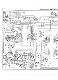
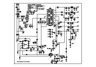
NOTES OF SCHEMATIC DIAGRAM<br />
Safety precautions<br />
The Components in<strong>de</strong>ntified by the symbol ! are<br />
critical for safety. For continued safety, replace safety<br />
critical components only with manufacturer's recommen<strong>de</strong>d<br />
parts.<br />
1. Units of components on the schematic diagram<br />
Unless otherwise specified.<br />
1) All resistance values are in ohm. 1/6 W, 1/8 W (refer to<br />
parts list).<br />
Chip resistors are 1/16 W.<br />
K: KΩ(1000Ω), M: MΩ (1000KΩ)<br />
2) All capacitance values are in µF, (P: PF).<br />
3) All inductance values are in µH, (m: mH).<br />
4) All dio<strong>de</strong>s are 1SS133, MA165 or 1N4148M (refer to parts<br />
list).<br />
Note: The Parts Number, value and rated voltage etc. in<br />
the Schematic Diagram are for references only.<br />
When replacing the parts, refer to the Parts List.<br />
2. Indications of control voltage<br />
AUX : Active at high.<br />
AUX or AUX(L) : Active at low.<br />
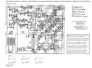
CHARTS AND DIAGRAMS<br />
4. Voltage measurement<br />
1) Regulator (DC/DC CONV) circuits<br />
REC : Colour bar signal.<br />
PB : Alignment tape (Colour bar).<br />
— : Unmeasurable or unnecessary to measure.<br />
2) Indication on schematic diagram<br />
Voltage indications for REC and PB mo<strong>de</strong> on the schematic<br />
diagram are as shown below.<br />
REC mo<strong>de</strong><br />
2.5<br />
(5.0)<br />
PB mo<strong>de</strong><br />
1 2 3<br />
1.8<br />
PB and REC mo<strong>de</strong>s<br />
(Voltage of PB and REC mo<strong>de</strong>s<br />
are the same)<br />
Note: If the voltages are not indicated on the schematic<br />
diagram, refer to the voltage charts.<br />
5. Signal path Symbols<br />
The arrows indicate the signal path as follows.<br />
NOTE : The arrow is DVC unique object.<br />
Playback signal path<br />
Playback and recording signal path<br />
CIRCUIT BOARD NOTES<br />
1. Foil and Component si<strong>de</strong>s<br />
1) Foil si<strong>de</strong> (B si<strong>de</strong>) :<br />
Parts on the foil si<strong>de</strong> seen from foil face (pattern face)<br />
are indicated.<br />
2) Component si<strong>de</strong> (A si<strong>de</strong>) :<br />
Parts on the component si<strong>de</strong> seen from component face<br />
(parts face) indicated.<br />
rts location are indicated by gui<strong>de</strong> scale on the circuit board.<br />
2. Parts location gui<strong>de</strong>s<br />
Parts location are indicated by gui<strong>de</strong> scale on the circuit board.<br />
B : Foil si<strong>de</strong><br />
(A : Component si<strong>de</strong>)<br />
C : Chip component<br />
D : Discrete component)<br />
REF No. LOCATION<br />
IC<br />
IC101 B C 6 A<br />
Category : IC<br />
Horizontal “A” zone<br />
Vertical “6” zone<br />
Note: For general information in service manual, please<br />
refer to the Service Manual of GENERAL INFORMA-<br />
TION Edition 4 No. 82054D (January 1994).<br />
3. Interpreting Connector indications<br />
Recording signal path<br />
(including E-E signal path)<br />
1<br />
2<br />
3<br />
Removable connector<br />
Capstan servo path<br />
Drum servo path<br />
1<br />
2<br />
3<br />
Wire sol<strong>de</strong>red directly on board<br />
(Example)<br />
R-Y<br />
Y<br />
Playback R-Y signal path<br />
Recording Y signal path<br />
1<br />
2<br />
3<br />
1<br />
2<br />
3<br />
4<br />
Non-removable Board connector<br />
Board to Board<br />
6. Indication of the parts for adjustments<br />
The parts for the adjustments are surroun<strong>de</strong>d with the circle<br />
as shown below.<br />
Connected pattern on board<br />
The arrows indicate signal path<br />
Note: For the <strong>de</strong>stination of each signal and further line<br />
connections that are cut off from the diagram,<br />
refer to "BOARD INTERCONNECTIONS"<br />
7. Indication of the parts not mounted on the circuit board<br />
“OPEN” is indicated by the parts not mounted on the circuit<br />
board.<br />
R216<br />
OPEN<br />
2-1 2-2