Fabrication of silicon microring resonator with smooth sidewalls
Fabrication of silicon microring resonator with smooth sidewalls
Fabrication of silicon microring resonator with smooth sidewalls

You also want an ePaper? Increase the reach of your titles
YUMPU automatically turns print PDFs into web optimized ePapers that Google loves.
Chen et al.: <strong>Fabrication</strong> <strong>of</strong> <strong>silicon</strong> <strong>microring</strong> <strong>resonator</strong> <strong>with</strong> <strong>smooth</strong> <strong>sidewalls</strong><br />
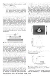
Fig. 1 Results obtained for fabricating <strong>silicon</strong> <strong>microring</strong> <strong>resonator</strong>s using different masking processes. a Cr mask etching; b maN-2403 mask<br />
etching; and c HSQ mask etching.<br />
They can be realized <strong>with</strong> diameters <strong>of</strong> less than 10 m,<br />
<strong>with</strong> negligible bending loss, which is essential for integration<br />
<strong>of</strong> micro- and nano-<strong>silicon</strong> photonics.<br />
<strong>Fabrication</strong> <strong>of</strong> <strong>silicon</strong> <strong>microring</strong> <strong>resonator</strong>s has been realized<br />
using various methods, principally by nanolithography<br />
followed by <strong>silicon</strong> etch technology, 7,8 but the process<br />
details have been only sparsely reported, especially aspects<br />
related to sidewall roughness control, which is crucial to<br />
suppress scattering loss in the <strong>resonator</strong>s. Normally, sidewall<br />
roughness is induced by a combination <strong>of</strong> transfer <strong>of</strong><br />
mask-edge roughness and etched surface roughness, the latter<br />
<strong>of</strong> which is the result <strong>of</strong> chemical reaction and ion bombardment<br />
on the <strong>silicon</strong> sidewall during the etch process. In<br />
the work discussed here, we present in detail the fabrication<br />
<strong>of</strong> <strong>silicon</strong> <strong>microring</strong> <strong>resonator</strong>s. Electron-beam lithography<br />
EBL and a lift-<strong>of</strong>f process were applied to form three<br />
different mask materials, chromium Cr, negative e-beam<br />
resist maN-2403, and hydrogen silsesquioxane HSQ, onto<br />
SOI wafers. Mask-edge roughness and its effect on the<br />
sidewall roughness <strong>of</strong> the <strong>resonator</strong>s were characterized<br />
and are discussed in the following. Subsequently, inductively<br />
coupled plasma ICP etch processes for <strong>silicon</strong> etching<br />
<strong>with</strong> various mask materials were developed and optimized<br />
<strong>with</strong> the aim to minimize etched surface roughness<br />
<strong>with</strong>out further post-etch process. Last, results obtained utilizing<br />
various mask materials were compared in order to<br />
achieve reduced process complexity, enhanced process latitude,<br />
and small sidewall roughness. In particular, <strong>silicon</strong><br />
<strong>microring</strong> <strong>resonator</strong>s <strong>with</strong> less than 10-nm sidewall roughness<br />
are demonstrated.<br />
2 Experiment<br />
Silicon <strong>microring</strong> <strong>resonator</strong>s were fabricated on SOI wafers<br />
consisting <strong>of</strong> a 320-nm-thick <strong>silicon</strong> top layer and a<br />
1-m-thick buffer oxide insulator layer. Etch mask patterns<br />
<strong>of</strong> the negative e-beam resists maN-2403 and HSQ were<br />
formed using a JEOL JBX-9300FS EBL system set to<br />
100-KV accelerating voltage and 2-nA exposure beam current.<br />
Exposure doses were optimized to achieve minimum<br />
linewidth fluctuation, while the Cr mask patterns were<br />
achieved by a lift-<strong>of</strong>f process consisting <strong>of</strong> EBL and a subsequent<br />
metal deposition process employing a CVC e-beam<br />
evaporator. Cr evaporation occurred at a pressure <strong>of</strong> less<br />
than 110 −6 Torr to ensure a sufficiently long mean free<br />
path <strong>of</strong> the Cr molecules for directional deposition.<br />
The etch process for patterning the <strong>silicon</strong> <strong>microring</strong><br />
<strong>resonator</strong>s was developed using a plasma-therm ICP tool.<br />
Both the ICP coil power and bias power, which separately<br />
control generation and direction <strong>of</strong> reactive ions, respectively,<br />
operate at radio frequency. Cl 2 and optional C 4 F 8<br />
were used as etch gases. Cl 2 is a common <strong>silicon</strong> etchant<br />
under plasma. C 4 F 8 helps to protect the phenolic resin<br />
polymer–based e-beam resist maN-2403, although it corrupts<br />
e-beam resist HSQ, which is a <strong>silicon</strong>-oxide-based<br />
J. Micro/Nanolith. MEMS MOEMS 043060-2<br />
Oct–Dec 2009/Vol. 84<br />
Downloaded from SPIE Digital Library on 28 Dec 2009 to 162.105.81.60. Terms <strong>of</strong> Use: http://spiedl.org/terms