Fabrication of silicon microring resonator with smooth sidewalls
Fabrication of silicon microring resonator with smooth sidewalls
Fabrication of silicon microring resonator with smooth sidewalls

Create successful ePaper yourself
Turn your PDF publications into a flip-book with our unique Google optimized e-Paper software.
J. Micro/Nanolith. MEMS MOEMS 84, 043060 Oct–Dec 2009<br />
<strong>Fabrication</strong> <strong>of</strong> <strong>silicon</strong> <strong>microring</strong> <strong>resonator</strong> <strong>with</strong><br />
<strong>smooth</strong> <strong>sidewalls</strong><br />
Yao Chen<br />
Guangxi University<br />
College <strong>of</strong> Physical Science and Technology<br />
Nanning, Guangxi, 530005, China<br />
and<br />
Huazhong University <strong>of</strong> Science and Technology<br />
Department <strong>of</strong> Electronic Science &<br />
Technology<br />
Wuhan, Hubei, 430074, China<br />
Junbo Feng<br />
Peking University<br />
State Key Laboratory on Advanced Optical<br />
Communication Systems and Networks<br />
Beijing, 100871, China<br />
Abstract. <strong>Fabrication</strong> <strong>of</strong> <strong>silicon</strong> <strong>microring</strong> <strong>resonator</strong>s was optimized by<br />
using electron-beam lithography EBL and inductively coupled plasma<br />
ICP etching <strong>with</strong> different mask materials. Sidewall roughness <strong>of</strong> less<br />
than 10 nm was revealed by high-resolution scanning electron microscopy<br />
SEM <strong>with</strong>out any post-etch process. The fabrication processes<br />
are described in detail, and comparisons are made in consideration <strong>of</strong><br />
process complexity, process latitude, and sidewall roughness. © 2009 Society<br />
<strong>of</strong> Photo-Optical Instrumentation Engineers. DOI: 10.1117/1.3258487<br />
Subject terms: <strong>microring</strong> <strong>resonator</strong>; fabrication; waveguide; roughness.<br />
Paper 08156RR received Oct. 8, 2008; revised manuscript received Sep. 9, 2009;<br />
accepted for publication Sep. 18, 2009; published online Nov. 13, 2009.<br />
Zhiping Zhou<br />
Peking University<br />
State Key Laboratory on Advanced Optical<br />
Communication Systems and Networks<br />
Beijing, 100871, China<br />
and<br />
Georgia Institute <strong>of</strong> Technology<br />
School <strong>of</strong> Electrical and Computer Engineering<br />
Atlanta, Georgia 30332-0250<br />
E-mail: zjzhou@pku.edu.cn<br />
Jun Yu<br />
Huazhong University <strong>of</strong> Science and Technology<br />
Department <strong>of</strong> Electronic Science &<br />
Technology<br />
Wuhan, Hubei, 430074, China<br />
Christopher J. Summers<br />
Georgia Institute <strong>of</strong> Technology<br />
School <strong>of</strong> Materials Science and Engineering<br />
Atlanta, Georgia 30332-0250<br />
David S. Citrin<br />
Georgia Institute <strong>of</strong> Technology<br />
School <strong>of</strong> Electrical and Computer Engineering<br />
Atlanta, Georgia 30332-0250<br />
and<br />
2958 Georgia Tech-CNRS<br />
Unité Mixte Internationale<br />
Georgia Tech Lorraine<br />
2 rue Marconi<br />
57070 Metz, France<br />
switching, 3 modulation, 4 wavelength conversion, 5 and<br />
1 Introduction<br />
utilized in various applications including filtering, 1,2 large refractive-index contrast between <strong>silicon</strong> and air.<br />
Microring <strong>resonator</strong>s have become a key building block for<br />
photonic integrated circuits due to their versatility in function<br />
and their capability <strong>of</strong> integration. They have been<br />
sensing. 6 Silicon <strong>microring</strong> <strong>resonator</strong>s, leveraging <strong>of</strong>f the<br />
mature <strong>silicon</strong>-on-insulator SOI platform, provide <strong>silicon</strong><br />
waveguides <strong>with</strong> strong lateral light confinement due to the<br />
1932-5150/2009/$25.00 © 2009 SPIE<br />
J. Micro/Nanolith. MEMS MOEMS 043060-1<br />
Oct–Dec 2009/Vol. 84<br />
Downloaded from SPIE Digital Library on 28 Dec 2009 to 162.105.81.60. Terms <strong>of</strong> Use: http://spiedl.org/terms
Chen et al.: <strong>Fabrication</strong> <strong>of</strong> <strong>silicon</strong> <strong>microring</strong> <strong>resonator</strong> <strong>with</strong> <strong>smooth</strong> <strong>sidewalls</strong><br />
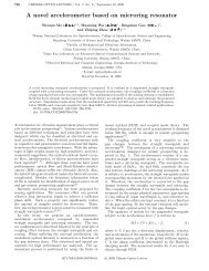
Fig. 1 Results obtained for fabricating <strong>silicon</strong> <strong>microring</strong> <strong>resonator</strong>s using different masking processes. a Cr mask etching; b maN-2403 mask<br />
etching; and c HSQ mask etching.<br />
They can be realized <strong>with</strong> diameters <strong>of</strong> less than 10 m,<br />
<strong>with</strong> negligible bending loss, which is essential for integration<br />
<strong>of</strong> micro- and nano-<strong>silicon</strong> photonics.<br />
<strong>Fabrication</strong> <strong>of</strong> <strong>silicon</strong> <strong>microring</strong> <strong>resonator</strong>s has been realized<br />
using various methods, principally by nanolithography<br />
followed by <strong>silicon</strong> etch technology, 7,8 but the process<br />
details have been only sparsely reported, especially aspects<br />
related to sidewall roughness control, which is crucial to<br />
suppress scattering loss in the <strong>resonator</strong>s. Normally, sidewall<br />
roughness is induced by a combination <strong>of</strong> transfer <strong>of</strong><br />
mask-edge roughness and etched surface roughness, the latter<br />
<strong>of</strong> which is the result <strong>of</strong> chemical reaction and ion bombardment<br />
on the <strong>silicon</strong> sidewall during the etch process. In<br />
the work discussed here, we present in detail the fabrication<br />
<strong>of</strong> <strong>silicon</strong> <strong>microring</strong> <strong>resonator</strong>s. Electron-beam lithography<br />
EBL and a lift-<strong>of</strong>f process were applied to form three<br />
different mask materials, chromium Cr, negative e-beam<br />
resist maN-2403, and hydrogen silsesquioxane HSQ, onto<br />
SOI wafers. Mask-edge roughness and its effect on the<br />
sidewall roughness <strong>of</strong> the <strong>resonator</strong>s were characterized<br />
and are discussed in the following. Subsequently, inductively<br />
coupled plasma ICP etch processes for <strong>silicon</strong> etching<br />
<strong>with</strong> various mask materials were developed and optimized<br />
<strong>with</strong> the aim to minimize etched surface roughness<br />
<strong>with</strong>out further post-etch process. Last, results obtained utilizing<br />
various mask materials were compared in order to<br />
achieve reduced process complexity, enhanced process latitude,<br />
and small sidewall roughness. In particular, <strong>silicon</strong><br />
<strong>microring</strong> <strong>resonator</strong>s <strong>with</strong> less than 10-nm sidewall roughness<br />
are demonstrated.<br />
2 Experiment<br />
Silicon <strong>microring</strong> <strong>resonator</strong>s were fabricated on SOI wafers<br />
consisting <strong>of</strong> a 320-nm-thick <strong>silicon</strong> top layer and a<br />
1-m-thick buffer oxide insulator layer. Etch mask patterns<br />
<strong>of</strong> the negative e-beam resists maN-2403 and HSQ were<br />
formed using a JEOL JBX-9300FS EBL system set to<br />
100-KV accelerating voltage and 2-nA exposure beam current.<br />
Exposure doses were optimized to achieve minimum<br />
linewidth fluctuation, while the Cr mask patterns were<br />
achieved by a lift-<strong>of</strong>f process consisting <strong>of</strong> EBL and a subsequent<br />
metal deposition process employing a CVC e-beam<br />
evaporator. Cr evaporation occurred at a pressure <strong>of</strong> less<br />
than 110 −6 Torr to ensure a sufficiently long mean free<br />
path <strong>of</strong> the Cr molecules for directional deposition.<br />
The etch process for patterning the <strong>silicon</strong> <strong>microring</strong><br />
<strong>resonator</strong>s was developed using a plasma-therm ICP tool.<br />
Both the ICP coil power and bias power, which separately<br />
control generation and direction <strong>of</strong> reactive ions, respectively,<br />
operate at radio frequency. Cl 2 and optional C 4 F 8<br />
were used as etch gases. Cl 2 is a common <strong>silicon</strong> etchant<br />
under plasma. C 4 F 8 helps to protect the phenolic resin<br />
polymer–based e-beam resist maN-2403, although it corrupts<br />
e-beam resist HSQ, which is a <strong>silicon</strong>-oxide-based<br />
J. Micro/Nanolith. MEMS MOEMS 043060-2<br />
Oct–Dec 2009/Vol. 84<br />
Downloaded from SPIE Digital Library on 28 Dec 2009 to 162.105.81.60. Terms <strong>of</strong> Use: http://spiedl.org/terms
Chen et al.: <strong>Fabrication</strong> <strong>of</strong> <strong>silicon</strong> <strong>microring</strong> <strong>resonator</strong> <strong>with</strong> <strong>smooth</strong> <strong>sidewalls</strong><br />
Fig. 2 Roughness at the edge <strong>of</strong> Cr mask.<br />
Fig. 4 Delamination <strong>of</strong> maN-2403 under Cl 2 plasma.<br />
polymer in which every <strong>silicon</strong> atom is bound to three oxygen<br />
atoms and one hydrogen atom <strong>with</strong> the exception <strong>of</strong> the<br />
terminal <strong>silicon</strong> atoms, since CF x generated from C 4 F 8 reacts<br />
<strong>with</strong> <strong>silicon</strong>-oxide-based material under plasma. C 4 F 8<br />
also <strong>of</strong>fers polymer protection at the sidewall <strong>of</strong> the etched<br />
<strong>silicon</strong>, thus reducing the striation roughness <strong>of</strong> the sidewall<br />
induced by ion bombardment under plasma. Cr has the<br />
greatest etch selectivity <strong>of</strong> <strong>silicon</strong> to the mask material<br />
compared <strong>with</strong> the preceeding e-beam resist due to its refractory<br />
metal property. We therefore used Cl 2 and C 4 F 8 for<br />
<strong>silicon</strong> etching <strong>of</strong> the maN-2403 and Cr mask which takes<br />
advantage <strong>of</strong> polymer protection for the etched <strong>silicon</strong> <strong>sidewalls</strong><br />
from C 4 F 8 , while we applied only Cl 2 for <strong>silicon</strong><br />
etching <strong>of</strong> the HSQ mask.<br />
The etching took place at a pressure <strong>of</strong> 5 mTorr, which<br />
is the lowest possible pressure in the system in order to<br />
pattern small features <strong>with</strong> vertical <strong>sidewalls</strong>. All etch recipes<br />
were optimized for <strong>silicon</strong> etching under the three different<br />
masks so as to obtain the highest selectivity <strong>of</strong> <strong>silicon</strong><br />
to each etch mask and to minimize sidewall roughness<br />
<strong>of</strong> the <strong>silicon</strong> <strong>microring</strong> <strong>resonator</strong>s. Experimental results<br />
were inspected using a Zeiss Ultra60 scanning electron microscope<br />
SEM <strong>with</strong> resolution down to 1 nm.<br />
3 Results and Discussion<br />
Silicon <strong>microring</strong> <strong>resonator</strong>s <strong>with</strong> diameter <strong>of</strong> 40 m,<br />
500-nm-wide waveguides, and 160-nm gaps were fabricated<br />
by EBL and ICP using the different mask materials.<br />
The results are shown in Fig. 1, in which Fig. 1a shows<br />
the result for Cr mask etching; Fig. 1b for negative<br />
e-beam resist maN-2403 mask etching; and Fig. 1c for<br />
negative e-beam resist HSQ mask etching.<br />
In the lift-<strong>of</strong>f process to create the Cr mask patterns,<br />
positive e-beam resist ZEP-520A was used as the sacrificial<br />
layer. Cr in the spacing areas other than the ring and the<br />
waveguides was intended to be removed in the resist strip<br />
process. Completely removing all the Cr at the edge <strong>of</strong> the<br />
ring and around the waveguide patterns proved very difficult,<br />
however, due to molecular forces. This results in severe<br />
edge roughness <strong>of</strong> the Cr mask, as shown in Fig. 2,<br />
and subsequently, the roughness is transferred to the etched<br />
<strong>silicon</strong> during the ICP process, which produces sidewall<br />
roughness on the <strong>silicon</strong> waveguides. The roughness is normally<br />
40 nm, determined by the roughness <strong>of</strong> the Cr<br />
mask. Figure 3 illustrates the sidewall roughness <strong>of</strong> the<br />
<strong>silicon</strong> waveguides transferred from the mask-edge roughness.<br />
In contrast, the mask-edge roughness <strong>of</strong> the negative<br />
e-beam resist maN-2403 and HSQ is relatively small, normally<br />
several nanometers, and is determined by the resist<br />
properties. Thus, the sidewall roughness results mainly<br />
from the etched surface roughness. The process <strong>with</strong> the Cr<br />
mask is slightly more complicated compared <strong>with</strong> the processes<br />
developed for the maN-2403 and HSQ masks, since<br />
an additional lift-<strong>of</strong>f step was applied to produce the Cr<br />
mask patterns. There is, however, considerable process latitude<br />
because <strong>of</strong> the extremely large etch selectivity <strong>of</strong> <strong>silicon</strong><br />
to Cr under plasma.<br />
On the other hand, processes based on the negative<br />
e-beam resists, maN-2403 and HSQ, are the simplest because<br />
they comprise only EBL and ICP etching. The etch<br />
selectivity <strong>of</strong> <strong>silicon</strong> to HSQ is much higher than that <strong>of</strong><br />
<strong>silicon</strong> to maN-2403 under Cl 2 plasma. This is because<br />
HSQ is a <strong>silicon</strong>-oxide-based material, while maN-2403 is<br />
composed <strong>of</strong> phenolic resin as a polymeric binder. Normally,<br />
the etch selectivity <strong>of</strong> <strong>silicon</strong> to maN-2403 is less<br />
Fig. 3 Silicon sidewall roughness.<br />
Fig. 5 Detail pr<strong>of</strong>ile <strong>of</strong> etched <strong>silicon</strong> sidewall. a Pr<strong>of</strong>ile <strong>of</strong> the<br />
etched <strong>silicon</strong> sidewall. b Edge fluctuation <strong>of</strong> the etched <strong>silicon</strong><br />
sidewall.<br />
J. Micro/Nanolith. MEMS MOEMS 043060-3<br />
Oct–Dec 2009/Vol. 84<br />
Downloaded from SPIE Digital Library on 28 Dec 2009 to 162.105.81.60. Terms <strong>of</strong> Use: http://spiedl.org/terms
Chen et al.: <strong>Fabrication</strong> <strong>of</strong> <strong>silicon</strong> <strong>microring</strong> <strong>resonator</strong> <strong>with</strong> <strong>smooth</strong> <strong>sidewalls</strong><br />
Fig. 6 Cross-section view <strong>of</strong> the fabricated <strong>silicon</strong> waveguide.<br />
Fig. 7 Silicon <strong>microring</strong> <strong>resonator</strong> <strong>with</strong> <strong>smooth</strong> <strong>sidewalls</strong>.<br />
than 1:1 under chlorine plasma, and it needs around<br />
400-nm-thick resist for etching 300-nm-thick <strong>silicon</strong>.<br />
Moreover, we observed that in some runs, the e-beam resist<br />
became delaminated by the Cl 2 plasma, as shown in Fig. 4.<br />
Due to the higher etch selectivity <strong>of</strong> Si to HSQ than that <strong>of</strong><br />
Si to maN-2403, thinner e-beam resist can be applied when<br />
using HSQ as mask material to improve EBL resolution<br />
and reduce mask-edge roughness. The etch selectivity <strong>of</strong><br />
<strong>silicon</strong> to HSQ is higher than 5:1, so in our experiment, the<br />
thickness <strong>of</strong> HSQ is 90 nm, and that <strong>of</strong> maN-2403 is<br />
300 nm for 320-nm-thick <strong>silicon</strong> etching by optimized ICP<br />
processes.<br />
Using our Cr and maN-2403 mask etch process, the<br />
etched surface roughness <strong>of</strong> the <strong>silicon</strong> <strong>microring</strong> <strong>resonator</strong>s<br />
is relatively low, normally less than 10 nm. This is due<br />
in part to the formation <strong>of</strong> the CF x polymer on the <strong>silicon</strong><br />
sidewall, which tends to reduce striation roughness associated<br />
<strong>with</strong> ion bombardment. The process <strong>with</strong> the HSQ<br />
masks permits considerable process latitude due to the high<br />
selectivity <strong>of</strong> <strong>silicon</strong> to HSQ. However, it is worthy <strong>of</strong> notice<br />
that only Cl 2 was used as the etching gas since C 4 F 8<br />
corrupts HSQ under plasma, and the striation roughness<br />
induced by ion bombardment on the <strong>silicon</strong> <strong>sidewalls</strong><br />
should be taken into consideration. Using the normal process,<br />
the etched surface roughness was 20 to 30 nm. In our<br />
process, we optimized the etch recipe based on HSQ mask<br />
etching and achieved etched surface roughness <strong>of</strong> less than<br />
10 nm, as shown in Fig. 5, where Fig. 5b is a top view <strong>of</strong><br />
the edge <strong>of</strong> the <strong>silicon</strong> waveguide, indicating roughness less<br />
than 10 nm. The roughness was demonstrated by inspecting<br />
the ripple edge fluctuation on top <strong>of</strong> the waveguide structure<br />
in a vertical etched pr<strong>of</strong>ile <strong>with</strong> high-resolution SEM.<br />
Using this method, it is essential to make sure that the<br />
Table 1 Comparison <strong>of</strong> various fabrication processes.<br />
Process<br />
complexity<br />
Process<br />
latitude<br />
Sidewall<br />
roughness<br />
Cr mask Complicated Excellent Rough<br />
maN-2403 mask Simple Poor Smooth<br />
HSQ mask Simple Good Smooth<br />
sidewall angle <strong>of</strong> the waveguide is close to 90 deg, and that<br />
there is no etch undercut below the etch mask, as shown in<br />
Fig. 6, so that the sidewall roughness can be demonstrated<br />
by the edge fluctuation on top <strong>of</strong> the waveguide. Since the<br />
edge fluctuation in Fig. 5b is around 5 nm, sidewall<br />
roughness less than 10 nm was achieved. The advantage <strong>of</strong><br />
the SEM inspection is that it can provide an approximate<br />
value <strong>of</strong> the roughness for the whole waveguide structure,<br />
which is essential for evaluating the optical scattering loss,<br />
but the limitation is that the definite value <strong>of</strong> the roughness<br />
cannot be detected by this method.<br />
A comparison was carried out for the preceding three<br />
processes considering process complexity, process latitude,<br />
and sidewall roughness <strong>of</strong> the <strong>resonator</strong>. The results are<br />
shown in Table 1.<br />
Last, by controlling the mask-edge roughness and the<br />
etched surface roughness, <strong>silicon</strong> <strong>microring</strong> <strong>resonator</strong>s were<br />
fabricated <strong>with</strong> an average sidewall roughness <strong>of</strong> less than<br />
10 nm, as shown in Fig. 7, which was demonstrated by<br />
inspecting the edge fluctuation <strong>of</strong> the waveguide structure<br />
in a vertical etched pr<strong>of</strong>ile <strong>with</strong> high-resolution SEM.<br />
These high-quality results could be achieved <strong>with</strong> both<br />
maN-2403- and HSQ-based processes, where the process<br />
<strong>with</strong> maN-2403 features the advantage <strong>of</strong> CF x sidewall protection<br />
etching, while that <strong>with</strong> HSQ takes advantage <strong>of</strong> the<br />
higher EBL resolution <strong>with</strong> thinner e-beam resist.<br />
4 Conclusion<br />
The process details <strong>of</strong> the fabrication <strong>of</strong> <strong>silicon</strong> <strong>microring</strong><br />
<strong>resonator</strong>s based on EBL and ICP etching were presented.<br />
Silicon sidewall roughness <strong>of</strong> less than 10 nm was achieved<br />
by accurate control <strong>of</strong> the mask-edge roughness and the<br />
etched surface roughness. Processes employing three different<br />
mask materials were discussed, analyzed, and compared<br />
to achieve reduced process complexity, enhanced process<br />
latitude, and low sidewall roughness <strong>of</strong> the fabricated <strong>resonator</strong>s.<br />
Acknowledgments<br />
This work is partially supported by the National Basic Research<br />
Program <strong>of</strong> China 2006CB708310 and the Natural<br />
Science Foundation <strong>of</strong> China 60578048. The work <strong>of</strong><br />
DSC was supported in part by the CNRS.<br />
J. Micro/Nanolith. MEMS MOEMS 043060-4<br />
Oct–Dec 2009/Vol. 84<br />
Downloaded from SPIE Digital Library on 28 Dec 2009 to 162.105.81.60. Terms <strong>of</strong> Use: http://spiedl.org/terms
Chen et al.: <strong>Fabrication</strong> <strong>of</strong> <strong>silicon</strong> <strong>microring</strong> <strong>resonator</strong> <strong>with</strong> <strong>smooth</strong> <strong>sidewalls</strong><br />
References<br />
1. P. P. Absil, J. V. Hryniewicz, B. E. Little, R. A. Wilson, L. G. Joneckis,<br />
and P.-T. Ho, “Compact <strong>microring</strong> notch filters,” IEEE Photon.<br />
Technol. Lett. 124, 398–400 2000.<br />
2. B. E. Little, S. T. Chu, H. A. Haus, J. Foresi, and J.-P. Laine, “Microring<br />
<strong>resonator</strong> channel dropping filters,” J. Lightwave Technol. 15,<br />
998–1005 1997.<br />
3. V. R. Almeida, C. A. Barrios, R. R. Panepucci, and M. Lipson, “Alloptical<br />
control <strong>of</strong> light on a <strong>silicon</strong> chip,” Nature (London) 431,<br />
1081–1083 2004.<br />
4. Q. F. Xu, B. Schmidt, S. Pradhan, and M. Lipson, “Micrometre-scale<br />
<strong>silicon</strong> electro-optic modulator,” Nature (London) 435, 325–327<br />
2005.<br />
5. P. P. Absil, J. V. Hryniewicz, B. E. Little, P. S. Cho, R. A. Wilson, L.<br />
G. Joneckis, and P.-T. Ho, “Wavelength conversion in GaAs <strong>microring</strong><br />
<strong>resonator</strong>s,” Opt. Lett. 25, 554–556 2000.<br />
6. Z. Xia, Y. Chen, and Z. Zhou, “Dual waveguide coupled <strong>microring</strong><br />
<strong>resonator</strong> sensor based on intensity detection,” IEEE J. Quantum<br />
Electron. 441, 100–107 2008.<br />
7. J. Niehusmann, A. Vorkel, P. H. Bolivar, T. Wahlbrink, W. Henschel,<br />
and H. Kurz, “Ultrahigh-quality-factor <strong>silicon</strong>-on-insulator <strong>microring</strong><br />
<strong>resonator</strong>,” Opt. Lett. 29, 2861–2863 2004.<br />
8. T. B. Jones, M. Hochberg, C. Walker, and A. Scherer, “High-Q ring<br />
<strong>resonator</strong>s in thin <strong>silicon</strong>-on-insulator,” Appl. Phys. Lett. 85, 3346–<br />
3347 2004.<br />
Yao Chen received his BS degree from<br />
Huzhong University <strong>of</strong> Science and Technology,<br />
China, in 2004, and he is now a PhD<br />
candidate in the Silicon Photonics and Microsystems<br />
Group at Wuhan National Laboratory<br />
for Optoelectronics. He has been<br />
working <strong>with</strong> Pr<strong>of</strong>. Zhou, Pr<strong>of</strong>. Summers,<br />
and Pr<strong>of</strong>. Yu on a joint project and focusing<br />
on fabrication <strong>of</strong> <strong>silicon</strong> <strong>microring</strong> <strong>resonator</strong><br />
and <strong>silicon</strong>-based photonic crystals. His research<br />
interests include fabrication for optoelectronics,<br />
semiconductor manufacturing technology, and MEMS<br />
technology.<br />
Junbo Feng received his BS degree from<br />
Huzhong University <strong>of</strong> Science and Technology,<br />
China, in 2004, and he is now a PhD<br />
candidate in the Silicon Photonics and Microsystems<br />
Group at Wuhan National Laboratory<br />
for Optoelectronics. His research interests<br />
include design and fabrication <strong>of</strong><br />
photonic devices, semiconductor manufacturing<br />
technology, and MEMS technology.<br />
Zhiping Zhou received his PhD EE degree<br />
from Georgia Institute <strong>of</strong> Technology<br />
GT in Atlanta in 1993. He was a founder<br />
and the vice president <strong>of</strong> production at<br />
Hengnan Transistor Factory in China 1971<br />
to 1978 and a guest scientist <strong>of</strong> NIST 1987<br />
to 1989. From 1993 to 2005, he was <strong>with</strong><br />
the Microelectronics Research Center at<br />
GT, where he engaged in research and development<br />
in the areas <strong>of</strong> semiconductor<br />
photonic devices. He is now a Changjiang<br />
pr<strong>of</strong>essor at Peking University, China, and also an adjunct pr<strong>of</strong>essor<br />
at the School <strong>of</strong> Electrical and Computer Engineering <strong>of</strong> GT. He is a<br />
senior member <strong>of</strong> IEEE, a member <strong>of</strong> SPIE, a member <strong>of</strong> OSA, and<br />
a life member <strong>of</strong> PSC.<br />
Jun Yu received his BS degree from Huazhong<br />
University <strong>of</strong> Science and Technology<br />
HUST in 1970, after which he worked<br />
as an assistant pr<strong>of</strong>essor in HUST. Subsequently,<br />
he was a visiting research scholar<br />
at Moscow University 1989 to 1990 and at<br />
Northwestern University 1998 to 1999. He<br />
became a pr<strong>of</strong>essor at HUST in 1996 and is<br />
currently the director <strong>of</strong> the Microelectronics<br />
Research Institute and vice director <strong>of</strong> the<br />
Beijing National Biochip Engineering Center.<br />
His multidisciplinary interests overlap the areas <strong>of</strong> novel ferroelectric<br />
materials and devices, MEMS, biochips and <strong>silicon</strong> thin-film<br />
solar cells. He is a senior member <strong>of</strong> the Chinese Institute <strong>of</strong> Electronics,<br />
a member <strong>of</strong> AAAS, and a member <strong>of</strong> MRS. He has earned<br />
numerous awards, holds 5 patents, and has over 130 publications.<br />
Christopher J. Summers received his BS<br />
and PhD in physics from Reading University<br />
in the UK. He has held positions at Bell<br />
Labs, GTE Labs, and McDonnell Douglas<br />
Research Labs. In 1981, he joined the<br />
Georgia Tech Research Institute and in<br />
1993 became director <strong>of</strong> the Phosphor<br />
Technology Center <strong>of</strong> Excellence. He is currently<br />
a pr<strong>of</strong>essor at the Georgia Tech<br />
School <strong>of</strong> Materials Science and Engineering<br />
and an adjunct faculty member in the<br />
Schools <strong>of</strong> Physics and Electrical and Computer Engineering. He<br />
has a research history in electro-optical materials characterization,<br />
molecular beam epitaxy <strong>of</strong> infrared and electronic materials, and the<br />
synthesis <strong>of</strong> phosphor materials for displays and solid-state lighting.<br />
His current research interests are in propagation through 2-D photonic<br />
crystals, such as self-collimation phenomena, giant refraction<br />
and superprism effects, and the use <strong>of</strong> 3-D photonic crystals infiltrated<br />
by atomic layer deposition for studying luminescence modification<br />
and tunability. He has received numerous awards and honors,<br />
holds 10 patents, and has over 300 publications.<br />
David S. Citrin was awarded a BA degree<br />
in physics, from Williams College, Massachusetts<br />
1985, after which he earned MS<br />
1987 and PhD 1991 degrees in physics<br />
from the University <strong>of</strong> Illinois at Urbana-<br />
Champaign, where he conducted theoretical<br />
research on the optical properties <strong>of</strong><br />
quantum wires. Subsequently, Citrin was a<br />
postdoctoral research fellow at the Max<br />
Planck Institute for Solid State Research,<br />
Stuttgart, Germany 1992 to 1993, where<br />
he worked on exciton radiative decay in low-dimensional semiconductor<br />
structures. From 1993 to 1995, he was Center fellow at the<br />
Center for Ultrafast Optical Science at the University <strong>of</strong> Michigan,<br />
where his work addressed ultrafast phenomena in quantum wells<br />
and microcavities. He was an assistant pr<strong>of</strong>essor <strong>of</strong> physics at<br />
Washington State University from 1995 to 2001, and received several<br />
pr<strong>of</strong>essional awards. Citrin is presently a pr<strong>of</strong>essor in the<br />
School <strong>of</strong> Electrical and Computer Engineering at the Georgia Institute<br />
<strong>of</strong> Technology. Areas <strong>of</strong> special focus include terahertz science<br />
and technology, semiconductor devices, nanoscale science and engineering,<br />
plasmonics, nonlinear optics, and ultrafast phenomena.<br />
J. Micro/Nanolith. MEMS MOEMS 043060-5<br />
Oct–Dec 2009/Vol. 84<br />
Downloaded from SPIE Digital Library on 28 Dec 2009 to 162.105.81.60. Terms <strong>of</strong> Use: http://spiedl.org/terms