Fabrication of silicon microring resonator with smooth sidewalls
Fabrication of silicon microring resonator with smooth sidewalls
Fabrication of silicon microring resonator with smooth sidewalls

You also want an ePaper? Increase the reach of your titles
YUMPU automatically turns print PDFs into web optimized ePapers that Google loves.
Chen et al.: <strong>Fabrication</strong> <strong>of</strong> <strong>silicon</strong> <strong>microring</strong> <strong>resonator</strong> <strong>with</strong> <strong>smooth</strong> <strong>sidewalls</strong><br />
Fig. 6 Cross-section view <strong>of</strong> the fabricated <strong>silicon</strong> waveguide.<br />
Fig. 7 Silicon <strong>microring</strong> <strong>resonator</strong> <strong>with</strong> <strong>smooth</strong> <strong>sidewalls</strong>.<br />
than 1:1 under chlorine plasma, and it needs around<br />
400-nm-thick resist for etching 300-nm-thick <strong>silicon</strong>.<br />
Moreover, we observed that in some runs, the e-beam resist<br />
became delaminated by the Cl 2 plasma, as shown in Fig. 4.<br />
Due to the higher etch selectivity <strong>of</strong> Si to HSQ than that <strong>of</strong><br />
Si to maN-2403, thinner e-beam resist can be applied when<br />
using HSQ as mask material to improve EBL resolution<br />
and reduce mask-edge roughness. The etch selectivity <strong>of</strong><br />
<strong>silicon</strong> to HSQ is higher than 5:1, so in our experiment, the<br />
thickness <strong>of</strong> HSQ is 90 nm, and that <strong>of</strong> maN-2403 is<br />
300 nm for 320-nm-thick <strong>silicon</strong> etching by optimized ICP<br />
processes.<br />
Using our Cr and maN-2403 mask etch process, the<br />
etched surface roughness <strong>of</strong> the <strong>silicon</strong> <strong>microring</strong> <strong>resonator</strong>s<br />
is relatively low, normally less than 10 nm. This is due<br />
in part to the formation <strong>of</strong> the CF x polymer on the <strong>silicon</strong><br />
sidewall, which tends to reduce striation roughness associated<br />
<strong>with</strong> ion bombardment. The process <strong>with</strong> the HSQ<br />
masks permits considerable process latitude due to the high<br />
selectivity <strong>of</strong> <strong>silicon</strong> to HSQ. However, it is worthy <strong>of</strong> notice<br />
that only Cl 2 was used as the etching gas since C 4 F 8<br />
corrupts HSQ under plasma, and the striation roughness<br />
induced by ion bombardment on the <strong>silicon</strong> <strong>sidewalls</strong><br />
should be taken into consideration. Using the normal process,<br />
the etched surface roughness was 20 to 30 nm. In our<br />
process, we optimized the etch recipe based on HSQ mask<br />
etching and achieved etched surface roughness <strong>of</strong> less than<br />
10 nm, as shown in Fig. 5, where Fig. 5b is a top view <strong>of</strong><br />
the edge <strong>of</strong> the <strong>silicon</strong> waveguide, indicating roughness less<br />
than 10 nm. The roughness was demonstrated by inspecting<br />
the ripple edge fluctuation on top <strong>of</strong> the waveguide structure<br />
in a vertical etched pr<strong>of</strong>ile <strong>with</strong> high-resolution SEM.<br />
Using this method, it is essential to make sure that the<br />
Table 1 Comparison <strong>of</strong> various fabrication processes.<br />
Process<br />
complexity<br />
Process<br />
latitude<br />
Sidewall<br />
roughness<br />
Cr mask Complicated Excellent Rough<br />
maN-2403 mask Simple Poor Smooth<br />
HSQ mask Simple Good Smooth<br />
sidewall angle <strong>of</strong> the waveguide is close to 90 deg, and that<br />
there is no etch undercut below the etch mask, as shown in<br />
Fig. 6, so that the sidewall roughness can be demonstrated<br />
by the edge fluctuation on top <strong>of</strong> the waveguide. Since the<br />
edge fluctuation in Fig. 5b is around 5 nm, sidewall<br />
roughness less than 10 nm was achieved. The advantage <strong>of</strong><br />
the SEM inspection is that it can provide an approximate<br />
value <strong>of</strong> the roughness for the whole waveguide structure,<br />
which is essential for evaluating the optical scattering loss,<br />
but the limitation is that the definite value <strong>of</strong> the roughness<br />
cannot be detected by this method.<br />
A comparison was carried out for the preceding three<br />
processes considering process complexity, process latitude,<br />
and sidewall roughness <strong>of</strong> the <strong>resonator</strong>. The results are<br />
shown in Table 1.<br />
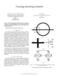
Last, by controlling the mask-edge roughness and the<br />
etched surface roughness, <strong>silicon</strong> <strong>microring</strong> <strong>resonator</strong>s were<br />
fabricated <strong>with</strong> an average sidewall roughness <strong>of</strong> less than<br />
10 nm, as shown in Fig. 7, which was demonstrated by<br />
inspecting the edge fluctuation <strong>of</strong> the waveguide structure<br />
in a vertical etched pr<strong>of</strong>ile <strong>with</strong> high-resolution SEM.<br />
These high-quality results could be achieved <strong>with</strong> both<br />
maN-2403- and HSQ-based processes, where the process<br />
<strong>with</strong> maN-2403 features the advantage <strong>of</strong> CF x sidewall protection<br />
etching, while that <strong>with</strong> HSQ takes advantage <strong>of</strong> the<br />
higher EBL resolution <strong>with</strong> thinner e-beam resist.<br />
4 Conclusion<br />
The process details <strong>of</strong> the fabrication <strong>of</strong> <strong>silicon</strong> <strong>microring</strong><br />
<strong>resonator</strong>s based on EBL and ICP etching were presented.<br />
Silicon sidewall roughness <strong>of</strong> less than 10 nm was achieved<br />
by accurate control <strong>of</strong> the mask-edge roughness and the<br />
etched surface roughness. Processes employing three different<br />
mask materials were discussed, analyzed, and compared<br />
to achieve reduced process complexity, enhanced process<br />
latitude, and low sidewall roughness <strong>of</strong> the fabricated <strong>resonator</strong>s.<br />
Acknowledgments<br />
This work is partially supported by the National Basic Research<br />
Program <strong>of</strong> China 2006CB708310 and the Natural<br />
Science Foundation <strong>of</strong> China 60578048. The work <strong>of</strong><br />
DSC was supported in part by the CNRS.<br />
J. Micro/Nanolith. MEMS MOEMS 043060-4<br />
Oct–Dec 2009/Vol. 84<br />
Downloaded from SPIE Digital Library on 28 Dec 2009 to 162.105.81.60. Terms <strong>of</strong> Use: http://spiedl.org/terms