ST7066 - Custom LCD Displays
ST7066 - Custom LCD Displays
ST7066 - Custom LCD Displays

You also want an ePaper? Increase the reach of your titles
YUMPU automatically turns print PDFs into web optimized ePapers that Google loves.
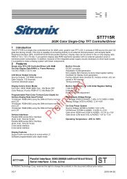
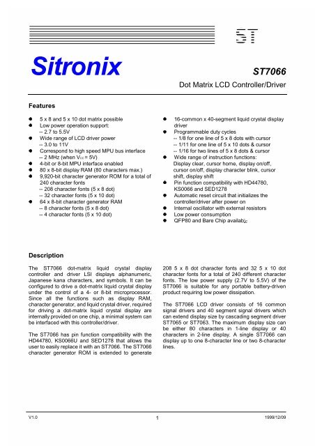
ST<br />
Sitronix<br />
<strong>ST7066</strong><br />
Dot Matrix <strong>LCD</strong> Controller/Driver<br />
Features<br />
z<br />
z<br />
z<br />
z<br />
z<br />
z<br />
z<br />
z<br />
5 x 8 and 5 x 10 dot matrix possible<br />
Low power operation support:<br />
-- 2.7 to 5.5V<br />
Wide range of <strong>LCD</strong> driver power<br />
-- 3.0 to 11V<br />
Correspond to high speed MPU bus interface<br />
-- 2 MHz (when VCC = 5V)<br />
4-bit or 8-bit MPU interface enabled<br />
80 x 8-bit display RAM (80 characters max.)<br />
9,920-bit character generator ROM for a total of<br />
240 character fonts<br />
-- 208 character fonts (5 x 8 dot)<br />
-- 32 character fonts (5 x 10 dot)<br />
64 x 8-bit character generator RAM<br />
-- 8 character fonts (5 x 8 dot)<br />
-- 4 character fonts (5 x 10 dot)<br />
z<br />
z<br />
z<br />
z<br />
z<br />
z<br />
z<br />
z<br />
16-common x 40-segment liquid crystal display<br />
driver<br />
Programmable duty cycles<br />
-- 1/8 for one line of 5 x 8 dots with cursor<br />
-- 1/11 for one line of 5 x 10 dots & cursor<br />
-- 1/16 for two lines of 5 x 8 dots & cursor<br />
Wide range of instruction functions:<br />
Display clear, cursor home, display on/off,<br />
cursor on/off, display character blink, cursor<br />
shift, display shift<br />
Pin function compatibility with HD44780,<br />
KS0066 and SED1278<br />
Automatic reset circuit that initializes the<br />
controller/driver after power on<br />
Internal oscillator with external resistors<br />
Low power consumption<br />
QFP80 and Bare Chip availabÿø<br />
Description<br />
The <strong>ST7066</strong> dot-matrix liquid crystal display<br />
controller and driver LSI displays alphanumeric,<br />
Japanese kana characters, and symbols. It can be<br />
configured to drive a dot-matrix liquid crystal display<br />
under the control of a 4- or 8-bit microprocessor.<br />
Since all the functions such as display RAM,<br />
character generator, and liquid crystal driver, required<br />
for driving a dot-matrix liquid crystal display are<br />
internally provided on one chip, a minimal system can<br />
be interfaced with this controller/driver.<br />
The <strong>ST7066</strong> has pin function compatibility with the<br />
HD44780, KS0066U and SED1278 that allows the<br />
user to easily replace it with an <strong>ST7066</strong>. The <strong>ST7066</strong><br />
character generator ROM is extended to generate<br />
208 5 x 8 dot character fonts and 32 5 x 10 dot<br />
character fonts for a total of 240 different character<br />
fonts. The low power supply (2.7V to 5.5V) of the<br />
<strong>ST7066</strong> is suitable for any portable battery-driven<br />
product requiring low power dissipation.<br />
The <strong>ST7066</strong> <strong>LCD</strong> driver consists of 16 common<br />
signal drivers and 40 segment signal drivers which<br />
can extend display size by cascading segment driver<br />
ST7065 or ST7063. The maximum display size can<br />
be either 80 characters in 1-line display or 40<br />
characters in 2-line display. A single <strong>ST7066</strong> can<br />
display up to one 8-character line or two 8-character<br />
lines.<br />
V1.0 1<br />
1999/12/09
<strong>ST7066</strong><br />
Block Diagram<br />
Reset<br />
Circuit<br />
26& 26& &/<br />
&/<br />
0<br />
CPG<br />
Timing<br />
Generator<br />
'<br />
56<br />
5:<br />
(<br />
MPU<br />
Interface<br />
Instruction<br />
Register (IR)<br />
Instruction<br />
Decoder<br />
Display<br />
data RAM<br />
(DDRAM)<br />
80x8 bits<br />
16-bit<br />
shift<br />
registe<br />
Common<br />
Signal<br />
Driver<br />
&20 WR<br />
&20<br />
'% WR<br />
'%<br />
'% WR<br />
'%<br />
Input/<br />
Output<br />
Buffer<br />
Data<br />
Register<br />
(DR)<br />
Address<br />
Counter<br />
40-bit<br />
shift<br />
registe<br />
40-bit<br />
latch<br />
circuit<br />
Segment<br />
Signal<br />
Driver<br />
<strong>LCD</strong> Drive<br />
Voltage<br />
Selector<br />
6(* WR<br />
6(*<br />
Busy<br />
Flag<br />
Character<br />
generator<br />
RAM<br />
(CGRAM)<br />
64 bits<br />
Character<br />
generator<br />
ROM<br />
(CGROM)<br />
9,920 bits<br />
Cursor<br />
and<br />
Blink<br />
controller<br />
*1'<br />
Parallel/Serial converter<br />
and<br />
Attribute Circuit<br />
9FF<br />
9 9 9 9 9<br />
V1.0 2<br />
1999/12/09
<strong>ST7066</strong><br />
Pad Arrangement<br />
<br />
<br />
<br />
<strong>ST7066</strong><br />
"<strong>ST7066</strong>" Marking : easy to find the PAD<br />
<br />
Chip Size : 2300x3000<br />
Coordinate : Pad Center<br />
Origin : Chip Center<br />
Pad Size : 90x90<br />
Unit : um<br />
<br />
<br />
V1.0 3<br />
1999/12/09
<strong>ST7066</strong><br />
Pad Location Coordinates<br />
ãô÷ áÁ Ùöü ë ì<br />
Ä æØÚÅÅ ÀÄÃÇà ÄÇÃÃ<br />
Å æØÚÅÄ ÀÄÃÇà ÄÅÊÃ<br />
Æ æØÚÅà ÀÄÃÇà ÄÄÇÃ<br />
Ç æØÚÄÌ ÀÄÃÇà ÄÃÅÃ<br />
È æØÚÄË ÀÄÃÇà ÌÃÃ<br />
É æØÚÄÊ ÀÄÃÇà ÊËÃ<br />
Ê æØÚÄÉ ÀÄÃÇà ÉÉÃ<br />
Ë æØÚÄÈ ÀÄÃÇà ÈÇÃ<br />
Ì æØÚÄÇ ÀÄÃÇà ÇÅÃ<br />
Äà æØÚÄÆ ÀÄÃÇà ÆÃÃ<br />
ÄÄ æØÚÄÅ ÀÄÃÇà ÄËÃ<br />
ÄÅ æØÚÄÄ ÀÄÃÇà ÉÃ<br />
ÄÆ æØÚÄà ÀÄÃÇà ÀÉÃ<br />
ÄÇ æØÚÌ ÀÄÃÇà ÀÄËÃ<br />
ÄÈ æØÚË ÀÄÃÇà ÀÆÃÃ<br />
ÄÉ æØÚÊ ÀÄÃÇà ÀÇÅÃ<br />
ÄÊ æØÚÉ ÀÄÃÇà ÀÈÇÃ<br />
ÄË æØÚÈ ÀÄÃÇà ÀÉÉÃ<br />
ÄÌ æØÚÇ ÀÄÃÇà ÀÊËÃ<br />
Åà æØÚÆ ÀÄÃÇà ÀÌÃÃ<br />
ÅÄ æØÚÅ ÀÄÃÇà ÀÄÃÅÃ<br />
ÅÅ æØÚÄ ÀÄÃÇà ÀÄÄÇÃ<br />
ÅÆ Úá× ÀÄÃÇÃ ÀÄÅÊÃ<br />
ÅÇ âæÖÄ ÀÄÃÇÃ ÀÄÇÃÃ<br />
ÅÈ âæÖÅ ÀÌÄÃ ÀÄÇÃÃ<br />
ÅÉ éÄ ÀÊËà ÀÄÇÃÃ<br />
ÅÊ éÅ ÀÉÉà ÀÄÇÃÃ<br />
ÅË éÆ ÀÈÇà ÀÄÇÃÃ<br />
ÅÌ éÇ ÀÇÅà ÀÄÇÃÃ<br />
Æà éÈ ÀÆÃà ÀÄÇÃÃ<br />
ÆÄ ÖßÄ ÀÄËà ÀÄÇÃÃ<br />
ÆÅ ÖßÅ ÀÉà ÀÄÇÃÃ<br />
ÆÆ éöö ÉÃ ÀÄÇÃÃ<br />
ÆÇ à ÄËÃ ÀÄÇÃÃ<br />
ÆÈ × ÆÃÃ ÀÄÇÃÃ<br />
ÆÉ åæ ÇÅÃ ÀÄÇÃÃ<br />
ÆÊ åê ÈÇÃ ÀÄÇÃÃ<br />
ÆË Ø ÉÉÃ ÀÄÇÃÃ<br />
ÆÌ ×ÕÃ ÊËÃ ÀÄÇÃÃ<br />
ÇÃ ×ÕÄ ÌÄÃ ÀÄÇÃÃ<br />
ãô÷ áÁ Ùöü ë ì<br />
ÇÄ ×ÕÅ ÄÃÇÃ ÀÄÇÃÃ<br />
ÇÅ ×ÕÆ ÄÃÇÃ ÀÄÅÊÃ<br />
ÇÆ ×ÕÇ ÄÃÇÃ ÀÄÄÇÃ<br />
ÇÇ ×ÕÈ ÄÃÇÃ ÀÄÃÅÃ<br />
ÇÈ ×ÕÉ ÄÃÇÃ ÀÌÃÃ<br />
ÇÉ ×ÕÊ ÄÃÇÃ ÀÊËÃ<br />
ÇÊ ÖâàÄ ÄÃÇà ÀÉÉÃ<br />
ÇË ÖâàÅ ÄÃÇà ÀÈÇÃ<br />
ÇÌ ÖâàÆ ÄÃÇà ÀÇÅÃ<br />
Èà ÖâàÇ ÄÃÇà ÀÆÃÃ<br />
ÈÄ ÖâàÈ ÄÃÇà ÀÄËÃ<br />
ÈÅ ÖâàÉ ÄÃÇà ÀÉÃ<br />
ÈÆ ÖâàÊ ÄÃÇà ÉÃ<br />
ÈÇ ÖâàË ÄÃÇà ÄËÃ<br />
ÈÈ ÖâàÌ ÄÃÇà ÆÃÃ<br />
ÈÉ ÖâàÄà ÄÃÇà ÇÅÃ<br />
ÈÊ ÖâàÄÄ ÄÃÇà ÈÇÃ<br />
ÈË ÖâàÄÅ ÄÃÇà ÉÉÃ<br />
ÈÌ ÖâàÄÆ ÄÃÇà ÊËÃ<br />
Éà ÖâàÄÇ ÄÃÇà ÌÃÃ<br />
ÉÄ ÖâàÄÈ ÄÃÇà ÄÃÅÃ<br />
ÉÅ ÖâàÄÉ ÄÃÇà ÄÄÇÃ<br />
ÉÆ æØÚÇà ÄÃÇà ÄÅÊÃ<br />
ÉÇ æØÚÆÌ ÄÃÇà ÄÇÃÃ<br />
ÉÈ æØÚÆË ÌÄà ÄÇÃÃ<br />
ÉÉ æØÚÆÊ ÊËà ÄÇÃÃ<br />
ÉÊ æØÚÆÉ ÉÉà ÄÇÃÃ<br />
ÉË æØÚÆÈ ÈÇà ÄÇÃÃ<br />
ÉÌ æØÚÆÇ ÇÅà ÄÇÃÃ<br />
Êà æØÚÆÆ ÆÃà ÄÇÃÃ<br />
ÊÄ æØÚÆÅ ÄËà ÄÇÃÃ<br />
ÊÅ æØÚÆÄ Éà ÄÇÃÃ<br />
ÊÆ æØÚÆà ÀÉà ÄÇÃÃ<br />
ÊÇ æØÚÅÌ ÀÄËà ÄÇÃÃ<br />
ÊÈ æØÚÅË ÀÆÃà ÄÇÃÃ<br />
ÊÉ æØÚÅÊ ÀÇÅà ÄÇÃÃ<br />
ÊÊ æØÚÅÉ ÀÈÇà ÄÇÃÃ<br />
ÊË æØÚÅÈ ÀÉÉà ÄÇÃÃ<br />
ÊÌ æØÚÅÇ ÀÊËà ÄÇÃÃ<br />
Ëà æØÚÅÆ ÀÌÄà ÄÇÃÃ<br />
V1.0 4<br />
1999/12/09
<strong>ST7066</strong><br />
Pin Functions<br />
NAME NUMBER I/O INTERFACED WITH FUNCTION<br />
RS 1 I MPU<br />
Select registers.<br />
0: Instruction register (for write) Busy flag:<br />
address counter (for read)<br />
1: Data register (for write and read)<br />
R/W 1 I MPU<br />
Select read or write.<br />
0: Write<br />
1: Read<br />
E 1 I MPU Starts data read/write.<br />
DB4 to DB7 4 I/O MPU<br />
Four high order bi-directional tristate data bus<br />
pins. Used for data transfer and receive<br />
between the MPU and the <strong>ST7066</strong>. DB7 can<br />
be used as a busy flag.<br />
DB0 to DB3 4 I/O MPU<br />
Four low order bi-directional tristate data bus<br />
pins. Used for data transfer and receive<br />
between the MPU and the <strong>ST7066</strong>.<br />
These pins are not used during 4-bit operation.<br />
CL1 1 O Extension driver<br />
Clock to latch serial data D sent to the<br />
extension driver<br />
CL2 1 O Extension driver Clock to shift serial data D<br />
M 1 O Extension driver<br />
Switch signal for converting the liquid crystal<br />
drive waveform to AC<br />
D 1 O Extension driver<br />
Character pattern data corresponding to each<br />
segment signal<br />
Common signals that are not used are changed<br />
to non-selection waveform. COM9 to COM16<br />
COM1 to COM16 16 O <strong>LCD</strong> are non-selection waveforms at 1/8 duty factor<br />
and COM12 to COM16 are non-selection<br />
waveforms at 1/11 duty factor.<br />
SEG1 to SEG40 40 O <strong>LCD</strong> Segment signals<br />
V1 to V5 5 - Power supply<br />
Power supply for <strong>LCD</strong> drive<br />
VCC - V5 = 11 V (Max)<br />
VCC , GND 2 - Power supply VCC : 2.7V to 5.5V, GND: 0V<br />
OSC1, OSC2 2<br />
When crystal oscillation is performed, a resistor<br />
Oscillation<br />
must be connected externally. When the pin<br />
resistor clock<br />
input is an external clock, it must be input to OSC1.<br />
Note:<br />
1. Vcc>=V1>=V2>=V3>=V4>=V5 must be maintained<br />
2. Two clock options:<br />
5 .<br />
9FF 9<br />
5 .<br />
26& 26& 26& 26&<br />
5<br />
&ORFN<br />
LQSXW<br />
V1.0 5<br />
1999/12/09
<strong>ST7066</strong><br />
FUNCTION DESCRIPTION<br />
System Interface<br />
This chip has all two kinds of interface type with MPU : 4-bit bus and 8-bit bus. 4-bit bus or 8-bit bus is selected by DL<br />
bit in the instruction register.<br />
During read or write operation, two 8-bit registers are used. One is data register (DR), the other is instruction<br />
register(IR).<br />
The data register(DR) is used as temporary data storage place for being written into or read from DDRAM/CGRAM,<br />
target RAM is selected by RAM address setting instruction. Each internal operation, reading from or writing into<br />
RAM, is done automatically. So to speak, after MPU reads DR data, the data in the next DDRAM/CGRAM address is<br />
transferred into DR automatically. Also after MPU writes data to DR, the data in DR is transferred into<br />
DDRAM/CGRAM automatically.<br />
The Instruction register(IR) is used only to store instruction code transferred from MPU. MPU cannot use it to read<br />
instruction data.<br />
To select register, use RS input pin in 4-bit/8-bit bus mode.<br />
Table 1. Various kinds of operations according to RS and R/W bits.<br />
56 5: 2SHUDWLRQ<br />
/ / ,QVWUXFWLRQ :ULWH RSHUDWLRQ 038 ZULWHV ,QVWUXFWLRQ FRGH<br />
LQWR ,5<br />
/ + 5HDG %XV\ )ODJ'% DQG DGGUHVV FRXQWHU '% a '%<br />
+ / 'DWD :ULWH RSHUDWLRQ 038 ZULWHV GDWD LQWR '5<br />
+ + 'DWD 5HDG RSHUDWLRQ 038 UHDGV GDWD IURP '5<br />
Busy Flag (BF)<br />
When BF = "High”, it indicates that the internal operation is being processed. So during this time the next instruction<br />
cannot be accepted. BF can be read, when RS = Low and R/W = High (Read Instruction Operation), through DB7<br />
port. Before executing the next instruction, be sure that BF is not High.<br />
Address Counter (AC)<br />
Address Counter(AC) stores DDRAM/CGRAM address, transferred from IR.<br />
After writing into (reading from) DDRAM/CGRAM, AC is automatically increased (decreased) by 1.<br />
When RS = "Low" and R/W = "High", AC can be read through DB0 ~ DB6 ports.<br />
V1.0 6<br />
1999/12/09
<strong>ST7066</strong><br />
Display Data RAM (DDRAM)<br />
Display data RAM (DDRAM) stores display data represented in 8-bit character codes. Its extended capacity is 80 x 8<br />
bits, or 80 characters. The area in display data RAM (DDRAM) that is not used for display can be used as general<br />
data RAM. See Figure 1 for the relationships between DDRAM addresses and positions on the liquid crystal display.<br />
The DDRAM address (ADD ) is set in the address counter (AC) as hexadecimal.<br />
z 1-line display (N = 0) (Figure 2)<br />
When there are fewer than 80 display characters, the display begins at the head position. For<br />
example, if using only the <strong>ST7066</strong>, 8 characters are displayed. See Figure 3.<br />
When the display shift operation is performed, the DDRAM address shifts. See Figure 3.<br />
+LJK 2UGHU<br />
ELWV<br />
/RZ 2UGHU<br />
ELWV<br />
([DPSOH ''5$0 $GGUHVV )<br />
$&<br />
AC6 AC5 AC4 AC3 AC2 AC1 AC0 1 0 0 1 1 1 1<br />
Ùüúø Ä ××åÔà Ô÷÷ø<br />
'LVSOD\<br />
3RVLWLRQ<br />
'LJLW<br />
DDRAM Address<br />
1 2 3 4 5 6 78 79 80<br />
00 01 02 03 04 05 ……………….. 4D 4E 4F<br />
Ùüúø Å ÄÀßüø ×üÿô<br />
'LVSOD\<br />
3RVLWLRQ<br />
''5$0<br />
$GGUHVV<br />
1 2 3 4 5 6 7 8<br />
00 01 02 03 04 05 06 07<br />
)RU<br />
6KLIW /HIW<br />
01 02 03 04 05 06 07<br />
08<br />
)RU<br />
6KLIW 5LJKW<br />
4F<br />
00 01 02 03 04 05 06<br />
Ùüúø Æ ÄÀßüø õ ËÀÖûôôöø ×üÿô Øô<br />
ÿø<br />
z 2-line display (N = 1) (Figure 4)<br />
V1.0 7<br />
1999/12/09
<strong>ST7066</strong><br />
Öôø ÄÍ êûø ûø õø ù÷üÿô öûôôöø ü ÿø ûô ÇÃ × 2 lines, the two lines are ÷üÿôø÷ ù ûø ûøô÷Á áø ûô<br />
ûø ùü ÿüø ø÷ ô÷÷ø ô÷ ûe second line start address are not consecutive. For øô ÿø¿ ûø ý ûø æçÊÃÉÉ ü<br />
ø÷¿ Ë öûôôöø × 2 lines are displayed. æøø Ùüúø ÈÁ<br />
V1.0 8<br />
1999/12/09
<strong>ST7066</strong><br />
êûø ÷üÿô ûüù øôü ü øù<br />
ø÷¿ ûø ××åÔà ô÷÷ø ûüùÁ æøø Ùüúø ÈÁ<br />
'LVSOD\<br />
3RVLWLRQ<br />
''5$0<br />
$GGUHVV<br />
KH[DGHFLPDO<br />
1 2 3 4 5 6<br />
00 01 02 03 04 05 ……………….. 25 26 27<br />
40 41 42 43 44 45 ……………….. 65 66 67<br />
38<br />
39<br />
40<br />
Ùüúø Ç<br />
ÅÀßüø ×üÿô<br />
'LVSOD\<br />
3RVLWLRQ<br />
''5$0<br />
$GGUHVV<br />
1 2 3 4 5 6 7 8<br />
00 01 02 03 04 05 06 07<br />
40 41 42 43 44 45 46 47<br />
)RU<br />
6KLIW /HIW<br />
01 02 03 04 05 06 07<br />
41 42 43 44 45 46 47<br />
08<br />
48<br />
)RU<br />
6KLIW 5LJKW<br />
27<br />
67<br />
00 01 02 03 04 05 06<br />
40 41 42 43 44 45 46<br />
Ùüúø È ÅÀßüø õ ËÀÖûôôöø ×üÿô Øô ÿø<br />
Öôø ÅÍÙ ô ÄÉÀöûôôöø × ÅÀÿüø ÷üÿô¿ ûø æçÊÃÉÉ öô õø øø÷ø÷ üú ø ÇÃÀ<br />
øøü ÷ü øÁ æøø Ùüúø ÉÁ<br />
êûø ÷üÿô ûüù øôü ü øù ø÷¿ ûø ××åÔà ô÷÷ø ûüùÁ æøø Ùüúø ÉÁ<br />
'LVSOD\<br />
3RVLWLRQ<br />
''5$0<br />
$GGUHVV<br />
1 2 3 4 5 6 7 8<br />
00 01 02 03 04 05 06 07<br />
40 41 42 43 44 45 46 47<br />
9 10 11 12 13 14 15 16<br />
08 09 0A 0B 0C 0D 0E 0F<br />
48 49 4A 4B 4C 4D 4E 4F<br />
)RU<br />
6KLIW<br />
/HIW<br />
01 02 03 04 05 06 07<br />
41 42 43 44 45 46 47<br />
08<br />
48<br />
09 0A 0B 0C 0D 0E 0F<br />
49 4A 4B 4C 4D 4E 4F<br />
10<br />
50<br />
)RU<br />
6KLIW<br />
5LJKW<br />
27<br />
67<br />
00 01 02 03 04 05 06<br />
40 41 42 43 44 45 46<br />
07<br />
47<br />
08 09 0A 0B 0C 0D 0E<br />
48 49 4A 4B 4C 4D 4E<br />
Ùüúø É ÅÀßüø õ ÄÉÀÖûôôöø ×üÿô Øô ÿø<br />
V1.0 9<br />
1999/12/09
<strong>ST7066</strong><br />
Character Generator ROM (CGROM)<br />
The character generator ROM generates 5 x 8 dot or 5 x 10 dot character patterns from 8-bit character codes. It can<br />
generate 208 5 x 8 dot character patterns and 32 5 x 10 dot character patterns. User-defined character patterns are<br />
also available by mask-programmed ROM.<br />
Character Generator RAM (CGRAM)<br />
In the character generator RAM, the user can rewrite character patterns by program. For 5 x 8 dots, eight character<br />
patterns can be written, and for 5 x 10 dots, four character patterns can be written.<br />
Write into DDRAM the character codes at the addresses shown as the left column of Table 4 to show the character<br />
patterns stored in CGRAM.<br />
See Table 5 for the relationship between CGRAM addresses and data and display patterns. Areas that are not used<br />
for display can be used as general data RAM.<br />
Timing Generation Circuit<br />
The timing generation circuit generates timing signals for the operation of internal circuits such as<br />
DDRAM, CGROM and CGRAM. RAM read timing for display and internal operation timing by MPU<br />
access are generated separately to avoid interfering with each other. Therefore, when writing data to<br />
DDRAM, for example, there will be no undesirable interference, such as flickering, in areas other than<br />
the display area.<br />
<strong>LCD</strong> Driver Circuit<br />
<strong>LCD</strong> Driver circuit has 16 common and 40 segment signals for <strong>LCD</strong> driving. Data from CGRAM/CGROM is<br />
transferred to 40 bit segment latch serially, and then it is stored to 40 bit shift latch. When each common is selected<br />
by 16 bit common register, segment data also output through segment driver from 40 bit segment latch. In case of<br />
1-line display mode, COM1 ~ COM8 have 1/8 duty or COM1 ~ COM11 have 1/11duty , and in 2-line mode, COM1 ~<br />
COM16 have 1/16 duty ratio.<br />
Cursor/Blink Control Circuit<br />
It can generate the cursor or blink in the cursor/blink control circuit. The cursor or the blink appears in the digit at the<br />
display data RAM address set in the address counter.<br />
V1.0 10<br />
1999/12/09
<strong>ST7066</strong><br />
Table 4 Correspondence between Character Codes and Character Patterns (ROM Code: 0A)<br />
V1.0 11<br />
1999/12/09
<strong>ST7066</strong><br />
Table 4(Cont.) (ROM Code: 0B)<br />
V1.0 12<br />
1999/12/09
<strong>ST7066</strong><br />
Character Code<br />
(DDRAM Data)<br />
CGRAM<br />
Address<br />
Character Patterns<br />
(CGRAM Data)<br />
b7 b6 b5 b4 b3 b3 b1 b0 b5 b4 b3 b2 b1 b0 b7 b6 b5 b4 b3 b2 b1 b0<br />
0 0 0 0 0 0 1 1 1 1 1<br />
0 0 0 0 -<br />
0 0 0 0 -<br />
0 0 0 0 0 1 0 0 1 0 0<br />
0 0 0 0 1 0 0 0 1 0 0<br />
0 0 0 0 1 1 0 0 1 0 0<br />
0 0 0<br />
- - -<br />
0 0 0 1 0 0 0 0 1 0 0<br />
0 0 0 1 0 1 0 0 1 0 0<br />
0 0 0 1 1 0 0 0 1 0 0<br />
0 0 0<br />
1 1 1<br />
0 0 0 0 0<br />
0 0 1 0 0 0 1 1 1 1 0<br />
0 0 1 0 0 1 1 0 0 0 1<br />
0 0 1 0 1 0 1 0 0 0 1<br />
0 0 1 0 1 1 1 1 1 1 0<br />
0 0 0<br />
- - -<br />
0 0 1 1 0 0 1 0 1 0 0<br />
0 0 1 1 0 1 1 0 0 1 0<br />
0 0 1 1 1 0 1 0 0 0 1<br />
0 0 1<br />
1 1 1<br />
0 0 0 0 0<br />
Table 5 Relationship between CGRAM Addresses, Character Codes (DDRAM) and Character patterns (CGRAM Data)<br />
Notes:<br />
1. Character code bits 0 to 2 correspond to CGRAM address bits 3 to 5 (3 bits: 8 types).<br />
2. CGRAM address bits 0 to 2 designate the character pattern line position. The 8th line is the<br />
cursor position and its display is formed by a logical OR with the cursor. Maintain the 8th line data, corresponding<br />
to the cursor display position, at 0 as the cursor display. If the 8th line data is 1, 1 bits will light up the 8th line<br />
regardless of the cursor presence.<br />
3. Character pattern row positions correspond to CGRAM data bits 0 to 4 (bit 4 being at the left).<br />
4. As shown Table 5, CGRAM character patterns are selected when character code bits 4 to 7 are<br />
all 0. However, since character code bit 3 has no effect, the R display example above can be selected by either<br />
character code 00H or 08H.<br />
5. 1 for CGRAM data corresponds to display selection and 0 to non-selection.<br />
“-“: Indicates no effect.<br />
V1.0 13<br />
1999/12/09
<strong>ST7066</strong><br />
Instructions<br />
çûøø ôø ù öôøúüø ùüöü ûôÍ<br />
z ×øüúôø æçÊÃÉÉ ùöü¿ öû ô ÷üÿô ù ô¿ ÷ôô ÿøúû¿ øöÁ<br />
z<br />
æø üøôÿ åÔà ô÷÷øø<br />
z ãøù ÷ôô ôùø üû üøôÿ åÔà<br />
z<br />
âûø<br />
Instruction Table:<br />
Instruction Code<br />
Instruction<br />
RS RW DB DB DB DB DB DB DB DB<br />
Description<br />
7 6 5 4 3 2 1 0<br />
Clear<br />
Write "20H" to DDRAM. and set<br />
0 0 0 0 0 0 0 0 0 1<br />
Display<br />
DDRAM address to "00H" from AC<br />
Return<br />
Home<br />
Entry Mode<br />
Set<br />
Display<br />
ON/OFF<br />
Cursor or<br />
Display<br />
Shift<br />
Function<br />
Set<br />
Set<br />
CGRAM<br />
address<br />
Set DDRAM<br />
address<br />
Read Busy<br />
flag and<br />
address<br />
Write data<br />
to RAM<br />
Read data<br />
from RAM<br />
0 0 0 0 0 0 0 0 1 x<br />
0 0 0 0 0 0 0 1 I/D S<br />
0 0 0 0 0 0 1 D C B<br />
0 0 0 0 0 1 S/C R/L x x<br />
0 0 0 0 1 DL N F x x<br />
0 0 0 1<br />
0 0 1<br />
0 1 BF<br />
AC<br />
6<br />
AC<br />
6<br />
AC AC<br />
5 4<br />
AC AC<br />
5 4<br />
AC AC<br />
5 4<br />
AC<br />
3<br />
AC<br />
3<br />
AC<br />
3<br />
AC<br />
2<br />
AC<br />
2<br />
AC<br />
2<br />
Set DDRAM address to "00H" from AC<br />
and return cursor to its original position<br />
if shifted. The contents of DDRAM are<br />
not changed.<br />
Sets cursor move direction and<br />
specifies display shift. These operations<br />
are performed during data write and<br />
read.<br />
D=1: entire display on<br />
C=1: cursor on<br />
B=1: cursor position on<br />
Set cursor moving and display shift<br />
control bit, and the direction, without<br />
changing DDRAM data.<br />
DL: interface data is 8/4 bits<br />
NL: number of line is 2/1<br />
F: font size is 5x11/5x8<br />
Set CGRAM address in address counter<br />
AC AC<br />
1 0<br />
AC AC Set DDRAM address in address counter<br />
1 0<br />
AC AC<br />
1 0<br />
1 0 D7 D6 D5 D4 D3 D2 D1 D0<br />
1 1 D7 D6 D5 D4 D3 D2 D1 D0<br />
Whether during internal operation or not<br />
can be known by reading BF. The<br />
contents of address counter can also be<br />
read.<br />
Write data into internal RAM<br />
(DDRAM/CGRAM)<br />
Read data from internal RAM<br />
(DDRAM/CGRAM)<br />
Description<br />
Time<br />
(270KHZ)<br />
1.52 ms<br />
1.52 ms<br />
Note:<br />
Be sure the <strong>ST7066</strong> is not in the busy state (BF = 0) before sending an instruction from the MPU to the <strong>ST7066</strong>.<br />
If an instruction is sent without checking the busy flag, the time between the first instruction and next instruction<br />
will take much longer than the instruction time itself. Refer to Instruction Table for the list of each instruction<br />
execution time.<br />
37 us<br />
37 us<br />
37 us<br />
37 us<br />
37 us<br />
37 us<br />
0 us<br />
43 us<br />
43 us<br />
V1.0 14<br />
1999/12/09
<strong>ST7066</strong><br />
INSTRUCTION DESCRIPTION<br />
z<br />
Clear Display<br />
RS<br />
RW<br />
DB7<br />
DB6<br />
DB5<br />
DB4<br />
DB3<br />
DB2<br />
DB1<br />
DB0<br />
&RGH<br />
0<br />
0<br />
0<br />
0<br />
0<br />
0<br />
0<br />
0<br />
0<br />
1<br />
z<br />
Clear all the display data by writing "20H" (space code) to all DDRAM address, and set DDRAM address to "00H"<br />
into AC (address counter). Return cursor to the original status, namely, bring the cursor to the left edge on first<br />
line of the display. Make entry mode increment (I/D = "1").<br />
Return Home<br />
RS<br />
RW<br />
DB7<br />
DB6<br />
DB5<br />
DB4<br />
DB3<br />
DB2<br />
DB1<br />
DB0<br />
&RGH<br />
0<br />
0<br />
0<br />
0<br />
0<br />
0<br />
0<br />
0<br />
1<br />
x<br />
z<br />
Return Home is cursor return home instruction. Set DDRAM address to "00H" into the address counter. Return<br />
cursor to its original site and return display to its original status, if shifted. Contents of DDRAM does not change.<br />
Entry Mode Set<br />
RS<br />
RW<br />
DB7<br />
DB6<br />
DB5<br />
DB4<br />
DB3<br />
DB2<br />
DB1 DB0<br />
&RGH<br />
0<br />
0<br />
0<br />
0<br />
0<br />
0<br />
0<br />
1<br />
I/D<br />
S<br />
Set the moving direction of cursor and display.<br />
I/D : Increment / decrement of DDRAM address (cursor or blink)<br />
When I/D = "High", cursor/blink moves to right and DDRAM address is increased by 1.<br />
When I/D = "Low", cursor/blink moves to left and DDRAM address is decreased by 1.<br />
* CGRAM operates the same as DDRAM, when read from or write to CGRAM.<br />
S: Shift of entire display<br />
When DDRAM read (CGRAM read/write) operation or S = "Low", shift of entire display is not performed. If S =<br />
"High" and DDRAM write operation, shift of entire display is performed according to I/D value (I/D = "1" : shift<br />
left, I/D = "0" : shift right).<br />
S I/D DESCRIPTION<br />
H H Shift the display to the left<br />
H L Shift the display to the right<br />
V1.0 15<br />
1999/12/09
<strong>ST7066</strong><br />
z<br />
Display ON/OFF<br />
RS<br />
RW<br />
DB7<br />
DB6<br />
DB5<br />
DB4<br />
DB3<br />
DB2<br />
DB1<br />
DB0<br />
&RGH<br />
0<br />
0<br />
0<br />
0<br />
0<br />
0<br />
1<br />
D<br />
C<br />
B<br />
Control display/cursor/blink ON/OFF 1 bit register.<br />
z<br />
D : Display ON/OFF control bit<br />
When D = "High", entire display is turned on.<br />
When D = "Low", display is turned off, but display data is remained in DDRAM.<br />
C : Cursor ON/OFF control bit<br />
When C = "High", cursor is turned on.<br />
When C = "Low", cursor is disappeared in current display, but I/D register remains its data.<br />
B : Cursor Blink ON/OFF control bit<br />
When B = "High", cursor blink is on, that performs alternate between all the high data and display character at<br />
the cursor position.<br />
When B = "Low", blink is off.<br />
Cursor or Display Shift<br />
RS<br />
RW<br />
DB7<br />
DB6<br />
DB5<br />
DB4<br />
DB3<br />
DB2<br />
DB1<br />
DB0<br />
&RGH<br />
0<br />
0<br />
0<br />
0<br />
0<br />
1<br />
S/C<br />
R/L<br />
x<br />
x<br />
Without writing or reading of display data, shift right/left cursor position or display. This instruction is used to<br />
correct or search display data. During 2-line mode display, cursor moves to the 2nd line after 40th digit of 1st line.<br />
Note that display shift is performed simultaneously in all the line. When displayed data is shifted repeatedly, each<br />
line shifted individually. When display shift is performed, the contents of address counter are not changed.<br />
S/C R/L Description AC Value<br />
L L Shift cursor to the left AC=AC-1<br />
L H Shift cursor to the right AC=AC+1<br />
H L Shift display to the left. Cursor follows the display shift AC=AC<br />
H H Shift display to the right. Cursor follows the display shift AC=AC<br />
z<br />
Function Set<br />
RS<br />
RW<br />
DB7<br />
DB6<br />
DB5<br />
DB4<br />
DB3<br />
DB2<br />
DB1 DB0<br />
&RGH<br />
0<br />
0<br />
0<br />
0<br />
1<br />
DL<br />
N<br />
F<br />
x<br />
x<br />
Control display/cursor/blink ON/OFF 1 bit register.<br />
V1.0 16<br />
1999/12/09
<strong>ST7066</strong><br />
DL : Interface data length control bit<br />
When DL = "High", it means 8-bit bus mode with MPU.<br />
When DL = "Low", it means 4-bit bus mode with MPU. So to speak, DL is a signal to select<br />
8-bit or 4-bit bus mode.<br />
When 4-bit bus mode, it needs to transfer 4-bit data by two times.<br />
N : Display line number control bit<br />
When N = "Low", it means 1-line display mode.<br />
When N = "High", 2-line display mode is set.<br />
F : Display font type control bit<br />
When F = "Low", it means 5 x 8 dots format display mode<br />
When F = "High", 5 x10 dots format display mode.<br />
No. of Display<br />
N<br />
F<br />
Character Font Duty Factor<br />
Lines<br />
L L 1 5x8 1/8<br />
L H 1 5x10 1/11<br />
H x 2 5x8 1/16<br />
z<br />
Set CGRAM Address<br />
RS RW DB7 DB6 DB5 DB4 DB3 DB2 DB1<br />
DB0<br />
&RGH<br />
0 0 0 1 AC5 AC4 AC3 AC2<br />
AC1 AC0<br />
z<br />
Set CGRAM address to AC.<br />
This instruction makes CGRAM data available from MPU.<br />
Set DDRAM Address<br />
RS RW DB7 DB6 DB5 DB4 DB3 DB2 DB1<br />
DB0<br />
&RGH<br />
0 0 1 AC6 AC5 AC4 AC3 AC2<br />
AC1 AC0<br />
Set DDRAM address to AC.<br />
This instruction makes DDRAM data available from MPU.<br />
When 1-line display mode (N = 0), DDRAM address is from "00H" to "4FH".<br />
In 2-line display mode (N = 1), DDRAM address in the 1st line is from "00H" to "27H", and<br />
DDRAM address in the 2nd line is from "40H" to "67H".<br />
V1.0 17<br />
1999/12/09
<strong>ST7066</strong><br />
z<br />
Read Busy Flag and Address<br />
RS<br />
RW<br />
DB7<br />
DB6<br />
DB5<br />
DB4<br />
DB3<br />
DB2<br />
DB1<br />
DB0<br />
&RGH<br />
1<br />
0<br />
D7<br />
D6<br />
D5<br />
D4<br />
D3<br />
D2<br />
D1<br />
D0<br />
z<br />
Write binary 8-bit data to DDRAM/CGRAM.<br />
The selection of RAM from DDRAM, CGRAM, is set by the previous address set instruction<br />
: DDRAM address set, CGRAM address set. RAM set instruction can also determine the AC<br />
direction to RAM.<br />
After write operation, the address is automatically increased/decreased by 1, according to<br />
the entry mode.<br />
Read Data from CGRAM or DDRAM<br />
RS<br />
RW<br />
DB7<br />
DB6<br />
DB5<br />
DB4<br />
DB3<br />
DB2<br />
DB1 DB0<br />
&RGH<br />
1<br />
1<br />
D7<br />
D6<br />
D5<br />
D4<br />
D3<br />
D2<br />
D1<br />
D0<br />
Read binary 8-bit data from DDRAM/CGRAM.<br />
The selection of RAM is set by the previous address set instruction. If address set instruction of RAM is not<br />
performed before this instruction, the data that read first is invalid, because the direction of AC is not determined.<br />
If you read RAM data several times without RAM address set instruction before read operation, you can get<br />
correct RAM data from the second, but the first data would be incorrect, because there is no time margin to<br />
transfer RAM data.<br />
In case of DDRAM read operation, cursor shift instruction plays the same role as DDRAM address<br />
set instruction : it also transfer RAM data to output data register. After read operation address counter is<br />
automatically increased/decreased by 1 according to the entry mode. After CGRAM read operation, display shift<br />
may not be executed correctly.<br />
* In case of RAM write operation, after this AC is increased/decreased by 1 like read operation. In this time, AC<br />
indicates the next address position, but you can read only the previous data by read instruction.<br />
V1.0 18<br />
1999/12/09
<strong>ST7066</strong><br />
Reset Function<br />
Initializing by Internal Reset Circuit<br />
An internal reset circuit automatically initializes the <strong>ST7066</strong> when the power is turned on. The<br />
following instructions are executed during the initialization. The busy flag (BF) is kept in the busy state<br />
until the initialization ends (BF = 1). The busy state lasts for 10 ms after VCC rises to 4.5 V.<br />
1. Display clear<br />
2. Function set:<br />
DL = 1; 8-bit interface data<br />
N = 0; 1-line display<br />
F = 0; 5 ´ 8 dot character font<br />
3. Display on/off control:<br />
D = 0; Display off<br />
C = 0; Cursor off<br />
B = 0; Blinking off<br />
4. Entry mode set:<br />
I/D = 1; Increment by 1<br />
S = 0; No shift<br />
Note:<br />
If the electrical characteristics conditions listed under the table Power Supply Conditions Using<br />
Internal Reset Circuit are not met, the internal reset circuit will not operate normally and will fail<br />
to initialize the <strong>ST7066</strong>. For such a case, initialization must be performed by the MPU as<br />
explain by the following figureÁ<br />
V1.0 19<br />
1999/12/09
<strong>ST7066</strong><br />
8-bit Interface:<br />
Power On<br />
Wait time > 15ms<br />
After Vcc > 4.5V<br />
RS RW D7 D6 D5 D4 D3 D2 D1 D0<br />
0 0 0 0 1 1 x x x x<br />
%) FDQQRW EH FKHFNHG<br />
EHIRUH WKH ,QVWUXFWLRQ<br />
)XQFWLRQ VHW<br />
Wait time > 4.1ms<br />
0 0 0 0 1 1 x x x x<br />
%) FDQQRW EH FKHFNHG<br />
EHIRUH WKH ,QVWUXFWLRQ<br />
)XQFWLRQ VHW<br />
Wait time > 100us<br />
0 0 0 0 1 1 x x x x<br />
%) FDQQRW EH FKHFNHG<br />
EHIRUH WKH ,QVWUXFWLRQ<br />
)XQFWLRQ VHW<br />
0 0 0 0 1 1 N F x x<br />
0 0 0 0 1 1 1 0 0 0<br />
0 0 0 0 0 0 0 0 0 1<br />
0 0 0 0 0 0 0 1 I/D S<br />
%) FDQ EH FKHFNHG DIWHU<br />
WKH IROORZLQJ<br />
,QVWUXFWLRQV<br />
)XQFWLRQ 6HW<br />
'LVSOD\ 2II<br />
'LVSOD\ &OHDU<br />
(QWU\ PRGH<br />
VHW<br />
Initialization End<br />
V1.0 20<br />
1999/12/09
<strong>ST7066</strong><br />
4-bit Interface:<br />
Power On<br />
Wait time > 15ms<br />
After Vcc > 4.5V<br />
RS RW D7 D6 D5 D4<br />
0 0 0 0 1 1<br />
%) FDQQRW EH FKHFNHG<br />
EHIRUH WKH ,QVWUXFWLRQ<br />
)XQFWLRQ VHW<br />
Wait time > 4.1ms<br />
0 0 0 0 1 1<br />
%) FDQQRW EH FKHFNHG<br />
EHIRUH WKH ,QVWUXFWLRQ<br />
)XQFWLRQ VHW<br />
Wait time > 100us<br />
0 0 0 0 1 1<br />
0 0 0 0 1 1<br />
0 0 0 0 1 1<br />
0 0 0 0 N F<br />
0 0 0 0 0 0<br />
0 0 1 0 0 0<br />
0 0 0 0 0 0<br />
0 0 0 0 0 1<br />
0 0 0 0 0 0<br />
0 0 0 1 I/D S<br />
%) FDQQRW EH FKHFNHG<br />
EHIRUH WKH ,QVWUXFWLRQ<br />
)XQFWLRQ VHW<br />
%) FDQ EH FKHFNHG DIWHU<br />
WKH IROORZLQJ<br />
,QVWUXFWLRQV<br />
)XQFWLRQ 6HW<br />
'LVSOD\ 2II<br />
'LVSOD\ &OHDU<br />
(QWU\ PRGH<br />
VHW<br />
Initialization End<br />
V1.0 21<br />
1999/12/09
<strong>ST7066</strong><br />
Interfacing to the MPU<br />
The <strong>ST7066</strong> can send data in either two 4-bit operations or one 8-bit operation, thus allowing interfacing with 4- or<br />
8-bit MPU.<br />
z For 4-bit interface data, only four bus lines (DB4 to DB7) are used for transfer. Bus lines DB0 to DB3 are<br />
disabled. The data transfer between the <strong>ST7066</strong> and the MPU is completed after the 4-bit data has been<br />
transferred twice. As for the order of data transfer, the four high order bits (for 8-bit operation, DB4 to DB7) are<br />
transferred before the four low order bits (for 8-bit operation, DB0 to DB3). The busy flag must be checked (one<br />
instruction) after the 4-bit data has been transferred twice. Two more 4-bit operations then transfer the busy flag<br />
and address counter data.<br />
z For 8-bit interface data, all eight bus lines (DB0 to DB7) are used.<br />
Supply Voltage for <strong>LCD</strong> Drive<br />
There are different voltages that supply to <strong>ST7066</strong>’s pin (V1 - V5) to obtain <strong>LCD</strong> drive waveform. The relations of the<br />
bias, duty factor and supply voltages are shown as below:<br />
Duty Factor<br />
1/8, 1/11 1/16<br />
Bias<br />
Supply Voltage 1/4 1/5<br />
V1 Vcc - 1/4V<strong>LCD</strong> Vcc - 1/5V<strong>LCD</strong><br />
V2 Vcc - 1/2V<strong>LCD</strong> Vcc - 2/5V<strong>LCD</strong><br />
V3 Vcc - 1/2V<strong>LCD</strong> Vcc - 3/5V<strong>LCD</strong><br />
V4 Vcc - 3/4V<strong>LCD</strong> Vcc - 4/5V<strong>LCD</strong><br />
V5 Vcc - V<strong>LCD</strong> Vcc- V<strong>LCD</strong><br />
ELDV<br />
GXW\<br />
F\FOH<br />
ELDV<br />
GXW\<br />
F\FOH<br />
9 9 9 9 9 9FF 9FF 9 9 9 9 9<br />
9 VR R R<br />
R R 9 R R R R R VR 9<br />
9/&'<br />
9/&'<br />
V1.0 22<br />
1999/12/09
<strong>ST7066</strong><br />
Timing Characteristics<br />
z<br />
Writing data from MPU to <strong>ST7066</strong><br />
56<br />
5:<br />
9,+<br />
9,/<br />
7$6<br />
7$+<br />
(<br />
73:<br />
7$+<br />
'%'%<br />
75<br />
7'6:<br />
9DOLG<br />
GDWD<br />
7&<br />
7+<br />
z<br />
Reading data from <strong>ST7066</strong> to MPU<br />
56<br />
5:<br />
9,+<br />
9,/<br />
7$6<br />
7$+<br />
75 73:<br />
7$+<br />
(<br />
7''5<br />
7+<br />
'%'%<br />
9DOLG<br />
GDWD<br />
7&<br />
V1.0 23<br />
1999/12/09
<strong>ST7066</strong><br />
Absolute Maximum Ratings<br />
Characteristics Symbol Value<br />
Power Supply Voltage V CC -0.3V to +7.0V<br />
<strong>LCD</strong> Driver Voltage V <strong>LCD</strong> -0.3V to +13.0V<br />
Input Voltage V IN -0.3V to V CC +0.3V<br />
Operating Temperature T A -20 o C to +60 o C<br />
Storage Temperature T STO -55 o C to +125 o C<br />
DC Characteristics (T A = 25 o C, V CC = 2.7V - 5.5V)<br />
Symbol Characteristics Test Condition Min. Typ. Max. Unit<br />
V CC Operating Voltage - 2.7 - 5.5 V<br />
V <strong>LCD</strong> <strong>LCD</strong> Voltage V CC -V5 3.0 - 11 V<br />
I CC Power Supply Current f OSC = 270KHz, V CC =5V - 0.3 0.6 mA<br />
V IH1<br />
V IL1<br />
V IH2<br />
V IL2<br />
V OH1<br />
V OL1<br />
V OH2<br />
V OL2<br />
Input High Voltage<br />
(Except OSC1)<br />
- 2.2 - V CC V<br />
Input Low Voltage<br />
- -0.3 - 0.6 V<br />
(Except OSC1)<br />
Input High Voltage<br />
- V CC -1 - V CC V<br />
(OSC1)<br />
Input Low Voltage<br />
- - - 1.0 V<br />
(OSC2)<br />
Output High Voltage I OH = -0.1mA 2.4 - V CC V<br />
(DB0 - DB7)<br />
Output Low Voltage I OL = 0.1mA - - 0.4 V<br />
(DB0 - DB7)<br />
Output High Voltage I OH = -0.04mA 0.9V CC - V CC V<br />
(Except DB0 - DB7)<br />
Output Low Voltage I OL = 0.04mA - - 0.1V CC V<br />
(Except DB0 - DB7)<br />
R COM Common Resistance V <strong>LCD</strong> = 4V, I d = 0.05mA - 2 20 KΩ<br />
R SEG Segment Resistance V <strong>LCD</strong> = 4V, I d = 0.05mA - 2 30 KΩ<br />
I LEAK<br />
Input Leakage V IN = 0V to V CC -1 - 1 µA<br />
Current<br />
I PUP Pull Up MOS Current V CC = 5V 10 50 120 µA<br />
V1.0 24<br />
1999/12/09
<strong>ST7066</strong><br />
AC Characteristics (T A = 25 o C, V CC = 5V)<br />
Symbol Characteristics Test Condition Min. Typ. Max. Unit<br />
Internal Clock Operation<br />
f OSC OSC Frequency R = 91KΩ 190 270 350 KHz<br />
External Clock Operation<br />
f EX External Frequency - 125 250 350 KHz<br />
Duty Cycle - 45 50 55 %<br />
T R ,T F Rise/Fall Time - - - 0.2 µs<br />
Write Mode (Writing data from MPU to <strong>ST7066</strong>)<br />
T C Enable Cycle Time Pin E 400 - - ns<br />
T PW Enable Pulse Width Pin E 150 - - ns<br />
T R ,T F Enable Rise/Fall Time Pin E - - 25 ns<br />
T AS Address Setup Time Pins: RS,RW,E 30 - - ns<br />
T AH Address Hold Time Pins: RS,RW,E 10 - - ns<br />
T DSW Data Setup Time Pins: DB0 - DB7 40 - - ns<br />
T H Data Hold Time Pins: DB0 - DB7 10 - - ns<br />
Read Mode (Reading Data from <strong>ST7066</strong> to MPU)<br />
T C Enable Cycle Time Pin E 400 - - ns<br />
T PW Enable Pulse Width Pin E 150 - - ns<br />
T R ,T F Enable Rise/Fall Time Pin E - - 25 ns<br />
T AS Address Setup Time Pins: RS,RW,E 30 - - ns<br />
T AH Address Hold Time Pins: RS,RW,E 10 - - ns<br />
T DDR Data Setup Time Pins: DB0 - DB7 - - 100 ns<br />
T H Data Hold Time Pins: DB0 - DB7 10 - - ns<br />
Interface Mode with <strong>LCD</strong> Driver(ST7065)<br />
T CWH Clock Pulse with High Pins: CL1, CL2 800 - - ns<br />
T CWL Clock Pulse with Low Pins: CL1, CL2 800 - - ns<br />
T CST Clock Setup Time Pins: CL1, CL2 500 - - ns<br />
T SU Data Setup Time Pin: D 300 - - ns<br />
T DH Data Hold Time Pin: D 300 - - ns<br />
T DM M Delay Time Pin: M -1000 - 1000 ns<br />
V1.0 25<br />
1999/12/09
<strong>ST7066</strong><br />
The relations between Oscillation Frequency and <strong>LCD</strong> Frame Frequency<br />
Assume the oscillation frequency is 270KHZ, 1 clock cycle time = 3.7us<br />
'XW\<br />
FORFNV<br />
COM1<br />
9FF<br />
<br />
<br />
9<br />
99<br />
9<br />
9<br />
IUDPH<br />
IUDPH XV [ [ XV<br />
PV<br />
'XW\<br />
FORFNV<br />
COM1<br />
9FF<br />
<br />
<br />
9<br />
99<br />
9<br />
9<br />
IUDPH<br />
IUDPH XV [ [ XV<br />
PV<br />
'XW\<br />
FORFNV<br />
COM1<br />
9FF<br />
<br />
<br />
9<br />
9<br />
9<br />
9<br />
9<br />
IUDPH<br />
IUDPH XV [ [ XV<br />
PV<br />
V1.0 26<br />
1999/12/09
<strong>ST7066</strong><br />
I/O PAD Configuration<br />
Input PAD: E (No Pull-up)<br />
Input PAD: RS, RW(with Pull-up)<br />
Output PAD: CL1, CL2, M, D<br />
(QDEOH<br />
'$7$<br />
I/O PAD: DB0 – DB7<br />
V1.0 27<br />
1999/12/09
<strong>ST7066</strong><br />
<strong>LCD</strong> and <strong>ST7066</strong> Connection<br />
1. 5x8 dots, 8 characters x 1 line (1/4 bias, 1/8 duty)<br />
&20<br />
<br />
<br />
<br />
<br />
<br />
&20<br />
67<br />
6(*<br />
<br />
<br />
<br />
6(*<br />
/&' 3DQHO &KDUDFWHUV<br />
[ OLQH<br />
2. 5x11 dots, 8 characters x 1 line (1/4 bias, 1/11 duty)<br />
67<br />
&20<br />
<br />
<br />
<br />
<br />
<br />
<br />
<br />
<br />
&20<br />
6(*<br />
<br />
<br />
<br />
<br />
<br />
<br />
<br />
6(*<br />
/&' 3DQHO &KDUDFWHUV<br />
[ OLQH<br />
V1.0 28<br />
1999/12/09
<strong>ST7066</strong><br />
3. 5x8 dots, 8 characters x 2 line (1/5 bias, 1/16 duty)<br />
&20<br />
<br />
<br />
<br />
<br />
<br />
&20<br />
67<br />
&20<br />
<br />
<br />
<br />
<br />
<br />
&20<br />
6(*<br />
<br />
<br />
<br />
<br />
<br />
<br />
<br />
6(*<br />
/&' 3DQHO &KDUDFWHUV<br />
[ OLQH<br />
4. 5x8 dots, 16 characters x 1 line (1/5 bias, 1/16 duty)<br />
&20<br />
<br />
<br />
<br />
<br />
<br />
&20<br />
67<br />
6(*<br />
<br />
<br />
<br />
<br />
6(*<br />
&20<br />
<br />
<br />
<br />
<br />
<br />
&20<br />
/&' 3DQHO <br />
&KDUDFWHUV [ OLQH<br />
V1.0 29<br />
1999/12/09
<strong>ST7066</strong><br />
<strong>ST7066</strong> Application circuit<br />
&20<br />
67<br />
'%'%<br />
7R 038<br />
6(*<br />
'<br />
9&&<br />
*1'<br />
&/<br />
&/<br />
0<br />
9<br />
9<br />
9<br />
9<br />
9<br />
9FF9<br />
<br />
'RW 0DWUL[ /&' 3DQHO<br />
'/<br />
9''<br />
)&6<br />
6+/<br />
6+/<br />
*1'<br />
9((<br />
9<br />
9<br />