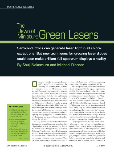
The Dawn of Miniature Green Laseres - Scientific American Digital
The Dawn of Miniature Green Laseres - Scientific American Digital
The Dawn of Miniature Green Laseres - Scientific American Digital
Create successful ePaper yourself
Turn your PDF publications into a flip-book with our unique Google optimized e-Paper software.
materials science<br />
<strong>The</strong><br />
<strong>Dawn</strong> <strong>of</strong><br />
<strong>Miniature</strong><br />
<strong>Green</strong> Lasers<br />
Semiconductors can generate laser light in all colors<br />
except one. But new techniques for growing laser diodes<br />
could soon make brilliant full-spectrum displays a reality<br />
By Shuji Nakamura and Michael Riordan<br />
Key Concepts<br />
■ ■ Solid-state lasers can produce<br />
light in the red and<br />
blue parts <strong>of</strong> the spectrum<br />
but not the green.<br />
■ ■ Recent research suggests<br />
that this “green gap”<br />
could be plugged as early<br />
as this year.<br />
■ ■ <strong>The</strong> advance will allow for<br />
laser-based video displays<br />
that are small enough to<br />
fit in a cell phone.<br />
—<strong>The</strong> Editors<br />
On a rainy Saturday morning in January<br />
2007, Henry Yang, chancellor <strong>of</strong> the<br />
University <strong>of</strong> California, Santa Barbara,<br />
took an urgent phone call. He excused himself<br />
abruptly from a meeting, grabbed his coat and<br />
umbrella, and rushed across the windswept<br />
U.C.S.B. campus to the Solid State Lighting and<br />
Display Center. <strong>The</strong> research group there included<br />
one <strong>of</strong> us (Nakamura), who had just received<br />
the Millennium Technology Prize for creating<br />
the first light-emitting diodes (LEDs) that emit<br />
bright blue light. Since that breakthrough over a<br />
decade earlier, Nakamura had continued his pioneering<br />
research on solid-state (semiconductor)<br />
lighting, developing green LEDs and the blue laser<br />
diodes that are now at the core <strong>of</strong> modern<br />
Blu-ray disc players.<br />
As Yang reached the center about 10 minutes<br />
later, people were milling about a small test lab.<br />
“Shuji had just arrived and was standing there in<br />
his leather jacket asking questions,” he recalled.<br />
Nakamura’s colleagues Steven DenBaars and<br />
James C. Speck were speaking with a few graduate<br />
students and postdoctoral researchers as<br />
they took turns looking into a microscope. <strong>The</strong>y<br />
parted for Yang, who peered into the eyepiece to<br />
witness a brilliant blue-violet flash emanating<br />
from a glassy chip <strong>of</strong> gallium nitride (GaN).<br />
Within days another group <strong>of</strong> researchers at<br />
Rohm Company in Kyoto, Japan—a partner in<br />
the U.C.S.B. center—duplicated the feat using<br />
similar materials. Although blue laser diodes are<br />
not in themselves very revolutionary [see “Blue-<br />
Laser CD Technology,” by Robert L. Gunshor<br />
and Arto V. Nurmikko; <strong>Scientific</strong> <strong>American</strong>,<br />
July 1996], Nichia Chemical Industries (based<br />
in Tokushima, Japan, where Nakamura worked<br />
until 2000), Sony and other companies were still<br />
struggling to produce inexpensive GaN laser devices<br />
for the Blu-ray disc market. <strong>The</strong>se diodes<br />
had previously been fashioned using a method<br />
with stubborn limitations that have kept manufacturing<br />
yields down and diode costs high.<br />
<strong>The</strong> groups from U.C.S.B. and Rohm are developing<br />
a new way to grow the crystalline layers<br />
<strong>of</strong> gallium nitride and related alloys that<br />
make up a laser diode. <strong>The</strong> early successes <strong>of</strong> the<br />
approach not only promise greater yields but<br />
also buoy hopes <strong>of</strong> an even bigger pay<strong>of</strong>f: rugged,<br />
compact GaN diodes that emit green laser<br />
light—a goal that has long eluded scientists and<br />
engineers. <strong>The</strong> technique should also lead to<br />
70 <strong>Scientific</strong> <strong>American</strong> © 2009 SCIENTIFIC AMERICAN, INC.<br />
April 2009
Caspar Benson<br />
high-efficiency green LEDs that emit much more<br />
light than existing devices.<br />
<strong>The</strong>se achievements would fill a gaping void<br />
in the visible spectrum where evolution has<br />
trained our eyes to be most sensitive, plugging<br />
the “green gap” in the red-green-blue triad needed<br />
for full-color laser projection and displays.<br />
<strong>The</strong>y should help speed the introduction <strong>of</strong> laser<br />
projectors for televisions and movie theaters—<br />
which will display much richer colors than other<br />
systems—and <strong>of</strong> tiny, handheld “pico projectors”<br />
to be used, for example, in cell phones.<br />
And high-power green diodes might even be employed<br />
in such diverse applications as DNA sequencing,<br />
industrial process control and underwater<br />
communications.<br />
A New Angle<br />
<strong>The</strong> key advance that led to bright blue solidstate<br />
lighting was the mid-1990s conversion to<br />
LEDs and laser diodes made <strong>of</strong> gallium nitride<br />
and its alloys [for a pr<strong>of</strong>ile <strong>of</strong> Nakamura, see<br />
“Blue Chip,” by Glenn Zorpette; <strong>Scientific</strong><br />
<strong>American</strong>, August 2000]. Before that, most<br />
researchers had focused their efforts on zinc<br />
selenide and related compounds. In the new<br />
approach, an exceedingly smooth, nanometersthin<br />
layer <strong>of</strong> indium gallium nitride (InGaN) is<br />
sandwiched between two layers <strong>of</strong> GaN, forming<br />
what is called a heterostructure or quantum<br />
well [see box on next page].<br />
By applying a suitable voltage, researchers set<br />
up an electric field perpendicular to these layers<br />
that drives electrons and holes—positively<br />
charged quasiparticles corresponding to the absence<br />
<strong>of</strong> electrons—together within the InGaN<br />
active layers. Inside this narrow trench, the electrons<br />
and holes recombine, annihilating one another<br />
and generating photons with an energy<br />
precisely determined by the properties <strong>of</strong> the active<br />
semiconductor material. By increasing the<br />
indium concentration in the alloy, one can lower<br />
this energy, thereby increasing the wavelength <strong>of</strong><br />
the light and changing its color from violet to<br />
blue to green.<br />
In LEDs the photons leave the well almost immediately,<br />
perhaps rebounding once or twice before<br />
exiting the device or being absorbed in the<br />
other layers. But in laser diodes, which produce<br />
coherent light, the photons stay largely confined<br />
within the trench. Two highly reflective mirrors—generally<br />
polished crystal surfaces at ei-<br />
What about<br />
<strong>Green</strong> Laser<br />
Pointers?<br />
<strong>The</strong> green lasers that have long<br />
been available employ a complicated<br />
two-step process to generate<br />
light. Semiconductor lasers inside<br />
these devices emit infrared radiation<br />
with a wavelength around<br />
1,060 nanometers. This radiation<br />
then pumps a crystal that oscillates<br />
at half this wavelength—about<br />
530 nanometers, solidly in the<br />
green. <strong>The</strong> process is costly, inefficient<br />
and imprecise—the second<br />
crystal can heat up, altering the<br />
wavelength <strong>of</strong> the resultant green<br />
light. Laser diodes that generate<br />
green light directly would avoid<br />
these problems.<br />
www.SciAm.com © 2009 SCIENTIFIC AMERICAN, INC.<br />
SCIENTIFIC AMERICAN 71
<strong>The</strong> <strong>Green</strong><br />
Gap problem<br />
Scientists have long been able to<br />
build semiconductor lasers that<br />
create light in red parts <strong>of</strong> the<br />
spectrum, and in the past decade<br />
they have conquered the blue<br />
and violet sections as well. Yet as<br />
they try to push these lasers into<br />
the green part <strong>of</strong> the spectrum,<br />
the amount <strong>of</strong> power produced<br />
drops precipitously.<br />
Laser Power<br />
400 500 600 700<br />
Wavelength (nanometers)<br />
[the basics]<br />
How Semiconductor Lasers Work<br />
Inside a solid-state laser, electrons meet positively charged entities<br />
called holes, annihilating one another and creating light. To adjust the<br />
ther end <strong>of</strong> it—recycle the photons back and<br />
forth inside, further stimulating electron-hole<br />
recombination. <strong>The</strong> laser light generated by this<br />
“stimulated emission” process is a tight pencil<br />
beam <strong>of</strong> exceedingly pure color.<br />
To make conventional GaN diodes, workers<br />
place a thin wafer <strong>of</strong> sapphire (or, increasingly,<br />
gallium nitride) inside a reaction chamber. <strong>The</strong>re<br />
hot gases deposit successive layers <strong>of</strong> gallium, indium<br />
and nitrogen atoms on that substrate, with<br />
the exact proportions <strong>of</strong> each element varying<br />
from layer to layer. <strong>The</strong> atoms in these layers automatically<br />
align with the existing crystalline<br />
structure, as predetermined by the substrate.<br />
Atom by atom, the layers grow in parallel with<br />
what is called the substrate’s c-plane, which is<br />
perpendicular to the crystal’s axis <strong>of</strong> hexagonal<br />
symmetry [see box on opposite page].<br />
Unfortunately, electrostatic forces and internal<br />
stresses between successive layers <strong>of</strong> positively<br />
charged gallium or indium ions and negatively<br />
charged nitrogen ions create strong electric fields<br />
perpendicular to the c-plane. <strong>The</strong>se fields, which<br />
can reach up to 100 volts per micron—equivalent<br />
to nearly 200 million volts across an average person’s<br />
height—counteract the applied external<br />
voltage. <strong>The</strong>y pull electrons away from holes—<br />
making it harder for them to recombine and yield<br />
light. In effect, the electrons pile up at one side <strong>of</strong><br />
the long quantum dance hall and holes at the other,<br />
both reluctant to cross over and meet.<br />
Known as the quantum-confined Stark effect,<br />
this nagging problem becomes particularly acute<br />
as the color <strong>of</strong> the emitted light shifts from violet<br />
to blue to green. And as the current through the<br />
diode increases, the greater number <strong>of</strong> charge<br />
carriers partially blocks the internal electric fields<br />
that keep electrons and holes apart. With these<br />
fields partially screened out, the electrons and<br />
holes then recombine at higher energies, shifting<br />
the light toward the blue end <strong>of</strong> the spectrum.<br />
<strong>The</strong>se problems are the main reason why green<br />
laser diodes and high-efficiency green LEDs have<br />
remained but a dream for more than a decade.<br />
(<strong>The</strong> familiar green laser pointers used by lecturers<br />
have semiconductor lasers that emit infrared<br />
radiation and pump another laser in a complicated,<br />
inefficient frequency-doubling scheme.)<br />
<strong>The</strong> approach pioneered by the U.C.S.B. and<br />
Rohm groups attempts to sidestep these prob-<br />
wavelength <strong>of</strong> this light, scientists must alter the material inside the<br />
semiconductor. But doing so can lead to other problems.<br />
Magnesiumdoped<br />
GaN<br />
Positive<br />
electrode<br />
Hole<br />
GaN barrier layer<br />
Substrate<br />
Silicon-doped<br />
GaN<br />
InGaN active layer<br />
Negative<br />
electrode<br />
layer cake<br />
Scientists create a diode laser by depositing layers <strong>of</strong> semiconductor<br />
material on top <strong>of</strong> an underlying substrate. On the bottom end<br />
<strong>of</strong> this semiconductor sandwich, gallium nitride (GaN) is mixed—or<br />
“doped”—with silicon impurities to produce an excess <strong>of</strong> negatively<br />
charged electrons. On the other end, GaN is doped with magnesium<br />
to give it an excess <strong>of</strong> positive charges, or “holes.” A voltage<br />
across the electrodes sets up an electric field that drives the<br />
electrons and holes together inside the central active layers.<br />
Electron<br />
INTERNAL AFFAIRS<br />
Inside these layers, electrons and<br />
GaN barrier layer<br />
holes annihilate to produce light (right).<br />
<strong>The</strong> wavelength <strong>of</strong> this light depends on the<br />
indium (In) content <strong>of</strong> the active layer—more leads<br />
to longer wavelengths and thus greener light. But the more<br />
indium in these layers, the more that indium is likely to pool into small<br />
“islands” during manufacture. <strong>The</strong> islands can alter the light’s wavelength—an<br />
unacceptable flaw in a laser.<br />
George RetseCk (semiconductor illustrations);<br />
scientific american (graph)<br />
72 <strong>Scientific</strong> <strong>American</strong> © 2009 SCIENTIFIC AMERICAN, INC.<br />
April 2009
[THE SOLUTION]<br />
A New Foundation<br />
A substrate is a slice <strong>of</strong> a crystal, and anything grown on top <strong>of</strong> it inherits its crystalline structure. <strong>The</strong> blue diode lasers that power Blu-ray disc<br />
players and PlayStation 3 game consoles are usually grown on top <strong>of</strong> sapphire, which, as substrates go, is relatively cheap and readily available.<br />
Yet it is difficult to use these substrates to make green laser diodes. In response, scientists have turned to alternative crystal facets for help.<br />
c-Plane: <strong>The</strong> Classic cut<br />
Though commonly used for blue lasers, a<br />
c-plane substrate has drawbacks, such as<br />
inducing electric fields that conspire to keep<br />
electrons and holes apart. <strong>The</strong> problem gets<br />
worse as the wavelength shifts toward green.<br />
m-Plane: A costly alternative<br />
Two research groups are growing laser diodes<br />
on a crystal’s m-plane, which cuts across the<br />
crystal’s side. Diodes grown on this plane do<br />
not suffer from induced fields, but the substrates<br />
are more costly than c-plane versions.<br />
semiPolar: <strong>The</strong> compromise<br />
A third option is semipolar substrates that are<br />
cut at a 45-degree angle to the crystal axis.<br />
<strong>The</strong>se substrates also do not produce strong<br />
fields, and they seem to yield better lasers and<br />
LEDs than the m-plane substrates do.<br />
RANDY LAMB University <strong>of</strong> California, Santa Barbara (Nakamura); COURTESY OF DONNA RIORDAN (Riordan); GEORGE RETSECK (crystals)<br />
beginning in 2000—including DenBaars and<br />
Speck at U.C.S.B. <strong>The</strong> early devices performed<br />
only modestly, mainly because <strong>of</strong> the lack <strong>of</strong><br />
high-quality GaN substrates. In 2006, however,<br />
Mitsubishi Chemical Corporation in Tokyo—<br />
another partner in the U.C.S.B. center—began<br />
supplying excellent, low-defect m-plane GaN<br />
substrates to the Rohm and U.C.S.B. research<br />
groups. Less than a centimeter on a side, the substrates<br />
were sliced from small GaN crystals<br />
about the size <strong>of</strong> a pencil eraser.<br />
With the new material in hand, Rohm and<br />
U.C.S.B. fabricated much more efficient LEDs<br />
in late 2006, and by early 2007 these groups began<br />
trying to make the more challenging laser<br />
diodes. On that rainy Saturday morning <strong>of</strong> January<br />
27, U.C.S.B. graduate student Matthew<br />
Schmidt went to the lab to finish the last fabrication<br />
step. <strong>The</strong>n he took the diode over to the<br />
nearby test lab and hitched it up to a power supply.<br />
Suddenly, as he cranked up the current flowing<br />
through the diode, a narrow beam <strong>of</strong> blueviolet<br />
light shot out <strong>of</strong> it.<br />
“Wow!” Schmidt thought. “I can finally<br />
graduate!”<br />
He called his thesis adviser DenBaars, who at<br />
first thought he was joking but soon alerted the<br />
rest <strong>of</strong> the group and Chancellor Yang. <strong>The</strong>y arrived<br />
within minutes to observe the surprising<br />
results. This first nonpolar GaN laser diode oplems<br />
by starting with a thin wafer <strong>of</strong> pure, crystalline<br />
GaN that has been sliced along a larger<br />
crystal’s m-plane [see box above] and then polished.<br />
Diodes fabricated on these so-called nonpolar<br />
substrates do not encounter the problems<br />
<strong>of</strong> conventional polar c-plane devices, because<br />
the troublesome fields caused by polarization<br />
and internal stresses are much lower.<br />
<strong>The</strong> diodes grown on GaN also produce light<br />
more efficiently than ones grown on sapphire because<br />
they suffer from far fewer crystalline defects—submicroscopic<br />
irregularities and mismatches<br />
at the interfaces between successive layers.<br />
Such defects act as centers where electrons<br />
and holes recombine to produce unwanted heat<br />
instead <strong>of</strong> light. <strong>The</strong>y can easily propagate upward<br />
through the successive diode layers during<br />
the growth process (in what are called threading<br />
dislocations) and reach the active layers. <strong>The</strong><br />
presence <strong>of</strong> these defects played havoc with production<br />
yields when Nichia and Sony first tried<br />
to manufacture blue laser diodes. Because a<br />
GaN substrate will generate nowhere near as<br />
many mismatches as sapphire does with the<br />
next-above layer <strong>of</strong> GaN or one <strong>of</strong> its alloys, diodes<br />
grown on nonpolar GaN substrates can<br />
therefore produce much more light—and have<br />
correspondingly less heat to dispose <strong>of</strong>.<br />
First suggested in the late 1990s, the nonpolar<br />
technique was attempted by several groups<br />
[<strong>The</strong> Authors]<br />
Shuji Nakamura is pr<strong>of</strong>essor in<br />
the materials department and<br />
director <strong>of</strong> the Solid-State Lighting<br />
and Energy Center at the University<br />
<strong>of</strong> California, Santa Barbara. He<br />
was awarded the 2006 Millennium<br />
Technology Prize for his work on<br />
blue laser diodes and LEDs.<br />
Michael Riordan teaches the<br />
history <strong>of</strong> physics and technology<br />
at Stanford University and at the<br />
University <strong>of</strong> California, Santa<br />
Cruz. He is co-author <strong>of</strong> Crystal<br />
Fire: <strong>The</strong> Invention <strong>of</strong> the Transistor<br />
and the Birth <strong>of</strong> the Information<br />
Age (W. W. Norton, 1997).<br />
www.SciAm.com © 2009 SCIENTIFIC AMERICAN, INC.<br />
SCIENTIFIC AMERICAN 73
erated at a wavelength <strong>of</strong> 405 nanometers (nm),<br />
as did the first Rohm device a few days later. And<br />
the currents flowing through these diodes were<br />
only two to three times what was then being<br />
achieved in commercially available devices made<br />
by Nichia and Sony, indicating that any heating<br />
problems were manageable.<br />
Going for <strong>Green</strong><br />
After that breakthrough, the U.C.S.B. group<br />
decided to drop most <strong>of</strong> its work on polar diodes<br />
and focus on nonpolar ones. It also began investigating<br />
a related strategy based on “semipolar”<br />
GaN substrates, which are wafers cut at an angle<br />
<strong>of</strong> about 45 degrees to a crystal’s major axis [see<br />
box on preceding page]. Diodes fabricated on<br />
semipolar substrates also have much less intense<br />
internal electric fields than polar diodes do,<br />
though not as low as in nonpolar diodes. <strong>The</strong><br />
U.C.S.B. researchers hope that one <strong>of</strong> these<br />
geometries will allow them to create the first<br />
green laser diodes and to make high-power<br />
LEDs at even longer wavelengths. Rohm has<br />
forged ahead in these areas, too, concentrating<br />
its efforts on nonpolar substrates.<br />
<strong>The</strong> new substrates, however, are not sufficient<br />
on their own to get beyond blue. <strong>Green</strong> diodes<br />
require adding more indium to the InGaN<br />
active layer, but the extra indium exacerbates internal<br />
stresses and disrupts the crystalline structure.<br />
It increases the number <strong>of</strong> crystal defects,<br />
which in turn reduces the light output and generates<br />
excess heat. While LEDs can still function<br />
despite the added defects, their efficiencies plummet<br />
as the color shifts from blue to green. Laser<br />
diodes are even more finicky and cannot tolerate<br />
so many defects. <strong>The</strong> highest wavelength thus<br />
far achieved in a laser diode is 488 nm, in the<br />
blue-green (or cyan) part <strong>of</strong> the spectrum.<br />
Layers <strong>of</strong> InGaN must also be grown at substantially<br />
lower temperatures—about 700<br />
degrees Celsius versus 1,000 degrees C for<br />
the GaN layers around it—to prevent the<br />
indium atoms from dissociating from the<br />
other atoms. Such dissociation can form areas<br />
<strong>of</strong> inhomogeneous indium alloys, or “islands,”<br />
which in turn causes the electron-hole recombination<br />
energy to vary from point to point. That<br />
variation makes the emission spectrum too<br />
broad to yield the coherent, monochromatic<br />
light expected from a laser. Thus, when workers<br />
raise the reactor temperature to grow the next<br />
GaN layer atop the delicate InGaN layer just deposited,<br />
they must be especially careful so as not<br />
to form too many <strong>of</strong> these islands. But the pro-<br />
[<strong>The</strong> Applications]<br />
H a n d h e l d Proj ec torS<br />
<strong>The</strong> smallest currently available handheld projectors are about the size <strong>of</strong> a remote control<br />
and use LEDs to generate light. By the end <strong>of</strong> this year the first laser-based models<br />
should go on sale. Even though they use frequency-doubling technology to create green<br />
laser light, they will produce high-resolution, richly colored images. Future models that<br />
rely on green laser diodes will allow for brighter and more efficient displays, and they<br />
will also shrink the projectors enough to allow them to fit inside your cell phone.<br />
Here is a look at two laser-based prototypes currently in development and<br />
a few LED projecters out now. —<strong>The</strong> Editors<br />
Microvision Show WX <br />
Inside this laser-projector protype, red,<br />
blue and green lasers focus onto a single<br />
mirror about the size <strong>of</strong> a pinhead. As<br />
light bounces <strong>of</strong>f that reflector, the mirror<br />
assembly rapidly scans back and forth to project<br />
pixels one by one onto a screen or wall. <strong>The</strong> lack <strong>of</strong><br />
lenses means the projector never needs to be focused.<br />
Resolution: 848 × 480 pixels (DVD-equivalent)<br />
Available: Later this year<br />
Light Blue Optics<br />
<strong>The</strong> start-up Light Blue Optics is also working on a laser projector. <strong>The</strong>se devices use<br />
liquid crystal on silicon (LCOS) chips that contain thousands <strong>of</strong> tiny liquid-crystal<br />
windows. <strong>The</strong> chip opens and closes these pixels in rapid succession to let light through<br />
and form an image. <strong>The</strong> company plans to have a laser-projection system ready for<br />
delivery to third-party manufacturers by the start <strong>of</strong> next year.<br />
Resolution: 854 × 480 pixels<br />
Available: 2010<br />
3M MPro110 <br />
When it debuted in 2008, the LED-based MPro110 was the<br />
first handheld projector to go on sale in the U.S. Although it<br />
is a bit larger than the Samsung MBP200 (below), this LCOS<br />
projector can display television-quality video. 3M is licensing an<br />
updated version <strong>of</strong> the technology that powers the MPro110 for<br />
use in other applications, such as cell phones.<br />
Resolution: 640 × 480 pixels (equivalent to standard-definition TV)<br />
Price: $359<br />
Samsung MBP200 Pico Projector<br />
This LED-based projector uses a miniaturized version <strong>of</strong> the digital light<br />
projection (DLP) chip from Texas Instruments. Light from a white<br />
LED first passes through a rapidly changing color wheel. It<br />
then hits an array <strong>of</strong> thousands <strong>of</strong> mirrors. Each mirror is<br />
about one-fifth the width <strong>of</strong> a human hair and switches<br />
on and <strong>of</strong>f thousands <strong>of</strong> times a second. Reflected light<br />
from this mirror forms the pixels that make up an image.<br />
Resolution: 480 × 320 pixels (approximately equivalent<br />
to a smart phone)<br />
Available: Later this year<br />
Toshiba LED pico Projector <br />
This LED competitor also uses the DLP chip technology.<br />
Resolution: 480 × 320 pixels<br />
Price: $399<br />
74 <strong>Scientific</strong> <strong>American</strong> © 2009 SCIENTIFIC AMERICAN, INC.<br />
April 2009
OPPOSITE PAGE: COURTESY OF MICROVISION, INC. (Show WX); COURTESY OF 3M, INC. (MPro110); COURTESY OF SAMSUNG (MBP200); COURTESY OF TOSHIBA (LED Pico Projector)<br />
cess gets ever more difficult as the indium concentration<br />
increases.<br />
<strong>The</strong> problems are exacerbated in polar diodes,<br />
in which the strong internal fields have led<br />
manufacturers to create active layers <strong>of</strong> InGaN<br />
that are exceedingly thin—less than 4 nm, or<br />
only about 20 atoms thick. This approach helps<br />
to keep electrons and holes huddled closer together,<br />
boosting the chances that they will meet<br />
and mate to create light. Because nonpolar and<br />
semipolar diodes have internal electric fields that<br />
are almost negligible, however, their InGaN active<br />
layers can be grown substantially thicker—<br />
up to 20 nm. <strong>The</strong> indium islands still form in<br />
these more robust layers, but they are thought to<br />
occur closer to the interfaces with the surrounding<br />
GaN. Confining the islands there should<br />
boost the chances <strong>of</strong> getting the narrower light<br />
spectrum needed for laser action. And the thicker,<br />
more robust active layers help to simplify<br />
manufacturing in other ways, allowing the elimination<br />
<strong>of</strong> extra “cladding” layers in the diode<br />
stack, which had formerly been added to help<br />
trap and guide the photons.<br />
Since the breakthrough demonstration in<br />
January 2007, the U.C.S.B. and Rohm groups<br />
have been steadily pushing back the frontiers <strong>of</strong><br />
the new technology, publishing new results almost<br />
every month. In April 2007, for example,<br />
U.C.S.B. reported a nonpolar LED emitting<br />
blue-violet light at 402 nm that achieved quantum<br />
efficiencies—the ratio <strong>of</strong> photons emitted<br />
to electrons flowing in—above 45 percent. This<br />
figure represented a 100-fold improvement in<br />
these devices in just a year. Several months later<br />
the group reported semipolar green LEDs that<br />
operated as high as 519 nm, with efficiencies<br />
close to 20 percent. (Unfortunately, these diodes<br />
experienced substantial blue shifts, for reasons<br />
that remain obscure.)<br />
More recently, U.C.S.B. fabricated yellow<br />
semipolar LEDs operating at 563 nm with efficiencies<br />
above 13 percent. <strong>The</strong>se were the first<br />
efficient yellow LEDs made with GaN and its<br />
alloys. Nonpolar laser diodes have also begun<br />
to approach the performance <strong>of</strong> their polar<br />
counterparts. In May 2008 Rohm reported<br />
achieving nonpolar laser diodes that operated<br />
at wavelengths as high as 481 nm—approaching<br />
the record <strong>of</strong> 488 nm held by polar diodes.<br />
<strong>The</strong> Big Time<br />
But fabricating a device in the laboratory is not<br />
the same as being able to manufacture it in commercial<br />
quantities. Probably the biggest road-<br />
Suddenly, as<br />
Schmidt cranked<br />
up the current<br />
flowing through<br />
the diode, a<br />
narrow beam<br />
<strong>of</strong> blue-violet<br />
light shot out<br />
<strong>of</strong> it. “Wow!” he<br />
thought. “I can<br />
finally graduate!”<br />
➥ More To<br />
Explore<br />
<strong>The</strong> Blue Laser Diode: <strong>The</strong> Complete<br />
Story. Second edition. Shuji<br />
Nakamura, Stephen Pearton and<br />
Gerhard Fasol. Springer, 2000.<br />
New GaN Faces Offer Brighter<br />
Emitters. Robert Metzger in<br />
Compound Semiconductor, Vol. 12,<br />
No. 7, pages 20–22; August 2006.<br />
Non-polar GaN Reaches Tipping<br />
Point. Steven DenBaars, Shuji<br />
Nakamura and Jim Speck in<br />
Compound Semiconductor, Vol. 13,<br />
No. 5, pages 21–23; June 2007.<br />
block to large-scale manufacture <strong>of</strong> nonpolar<br />
and semipolar GaN laser diodes and LEDs—<br />
whether violet, blue, green or yellow—is the<br />
availability <strong>of</strong> large enough substrates at acceptable<br />
costs. So far Mitsubishi has supplied GaN<br />
substrates about a square centimeter in surface<br />
area that are sliced from small crystals, but the<br />
wafer area needs to increase nearly 20-fold.<br />
To produce laser diodes economically, manufacturers<br />
must have substrates at least five centimeters<br />
in diameter costing about $2,000 per<br />
wafer, says Robert Walker, a semiconductor industry<br />
expert at Sierra Ventures in Menlo Park,<br />
Calif. To manufacture the simpler (and much<br />
cheaper) LEDs, he adds, substrate costs must<br />
drop by another order <strong>of</strong> magnitude. And these<br />
LEDs will still have to compete with advanced<br />
blue and green LEDs, such as those introduced<br />
in late 2007 by CREE Research in Durham,<br />
N.C. (also a partner in the U.C.S.B. center),<br />
which fabricates its devices on silicon-carbide<br />
substrates.<br />
Mitsubishi is now streamlining and scaling<br />
up its existing fabrication procedure in a move<br />
toward commercializing nonpolar GaN substrates.<br />
According to Kenji Fujito, who developed<br />
the methods used to grow nonpolar GaN<br />
substrates, it is a sluggish and painstaking process.<br />
At present, Mitsubishi can produce just<br />
enough nonpolar (or semipolar) GaN substrates<br />
to meet the research needs <strong>of</strong> Rohm and U.C.S.B.<br />
Fujito says it will be at least another year or two<br />
before they can produce substrate wafers five<br />
centimeters in diameter. Walker concurs, projecting<br />
that it should take a few years before nonpolar<br />
substrates will be economically available,<br />
either from Mitsubishi or other substrate suppliers,<br />
such as Kyma Technologies in Raleigh, N.C.<br />
But U.C.S.B.’s DenBaars expects commercial<br />
nonpolar diodes to be manufactured sooner, citing<br />
the higher yields and thus lower overall costs<br />
that these substrates should allow.<br />
In the meantime, lab work will continue to<br />
lead the way. Both the Rohm and U.C.S.B.<br />
groups, as well as several others, have set their<br />
sights on achieving the first successful green laser<br />
diodes. And in September 2008 U.C.S.B. reported<br />
observing stimulated emission at cyan (480<br />
nm) and green (514 nm) wavelengths from nonpolar<br />
and semipolar GaN diodes that had been<br />
optically pumped with light from another laser.<br />
Getting similar emissions using electric current<br />
to drive the diodes instead should not be too far<br />
<strong>of</strong>f. We would not be surprised to see one or both<br />
<strong>of</strong> these groups succeed later this year. ■<br />
www.SciAm.com © 2009 SCIENTIFIC AMERICAN, INC.<br />
SCIENTIFIC AMERICAN 75





![More Effective C++ [Meyers96]](https://img.yumpu.com/25323611/1/184x260/more-effective-c-meyers96.jpg?quality=85)
