74F74 - Dual D-type flip-flop
74F74 - Dual D-type flip-flop
74F74 - Dual D-type flip-flop

Create successful ePaper yourself
Turn your PDF publications into a flip-book with our unique Google optimized e-Paper software.
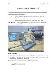
INTEGRATED CIRCUITS<br />
<strong>74F74</strong><br />
<strong>Dual</strong> D-<strong>type</strong> <strong>flip</strong>-<strong>flop</strong><br />
Product specification<br />
Supercedes data of 1990 Oct 23<br />
IC15 Data Handbook<br />
1996 Mar 12
Philips Semiconductors<br />
Product specification<br />
<strong>Dual</strong> D-<strong>type</strong> <strong>flip</strong>-<strong>flop</strong><br />
<strong>74F74</strong><br />
FEATURE<br />
• Industrial temperature range available (–40°C to +85°C)<br />
DESCRIPTION<br />
The <strong>74F74</strong> is a dual positive edge-triggered D-<strong>type</strong> <strong>flip</strong>-<strong>flop</strong> featuring<br />
individual data, clock, set, and reset inputs; also true and<br />
complementary outputs. Set (SD) and reset (RD) are asynchronous<br />
active low inputs and operate independently of the clock input. When<br />
set and reset are inactive (high), data at the D input is transferred to<br />
the Q and Q outputs on the low-to-high transition of the clock. Data<br />
must be stable just one setup time prior to the low-to-high transition of<br />
the clock for predictable operation. Clock triggering occurs at a<br />
voltage level and is not directly related to the transition time of the<br />
positive-going pulse. Following the hold time interval, data at the D<br />
input may be changed without affecting the levels of the output.<br />
PIN CONFIGURATION<br />
RD0 1<br />
D0 2<br />
CP0 3<br />
SD0 4<br />
Q0 5<br />
Q0 6<br />
GND 7<br />
14 V CC<br />
13 RD1<br />
12 D1<br />
11 CP1<br />
10 SD1<br />
9 Q1<br />
8 Q1<br />
SF00045<br />
TYPE TYPICAL f max TYPICAL SUPPLY CURRENT (TOTAL)<br />
<strong>74F74</strong> 125MHz 11.5mA<br />
ORDERING INFORMATION<br />
DESCRIPTION<br />
COMMERCIAL RANGE<br />
V CC = 5V ±10%,<br />
T amb = 0°C to +70°C<br />
ORDER CODE<br />
INDUSTRIAL RANGE<br />
V CC = 5V ±10%,<br />
T amb = –40°C to +85°C<br />
PKG. DWG. #<br />
14-pin plastic DIP N<strong>74F74</strong>N I<strong>74F74</strong>N SOT27-1<br />
14-pin plastic SO N<strong>74F74</strong>D I<strong>74F74</strong>D SOT108-1<br />
INPUT AND OUTPUT LOADING AND FAN OUT TABLE<br />
PINS DESCRIPTION 74F (U.L.) HIGH/LOW LOAD VALUE HIGH/LOW<br />
D0, D1 Data inputs 1.0/1.0 20µA/0.6mA<br />
CP0, CP1 Clock inputs (active rising edge) 1.0/1.0 20µA/0.6mA<br />
SD0, SD1 Set inputs (active low) 1.0/3.0 20µA/1.8mA<br />
RD0, RD1 Reset inputs (active low) 1.0/3.0 20µA/1.8mA<br />
Q0, Q1, Q0, Q1 Data outputs 50/33 1.0mA/20mA<br />
NOTE: One (1.0) FAST unit load is defined as: 20µA in the high state and 0.6mA in the low state.<br />
LOGIC SYMBOL<br />
IEC/IEEE SYMBOL<br />
2 12<br />
3<br />
4<br />
1<br />
CP0<br />
SD0<br />
RD0<br />
D0<br />
D1<br />
4<br />
3<br />
2<br />
1<br />
S<br />
C1<br />
1D<br />
R<br />
&<br />
5<br />
6<br />
11<br />
10<br />
13<br />
CP1<br />
SD1<br />
RD1<br />
Q0 Q0<br />
Q1 Q1<br />
10<br />
11<br />
12<br />
13<br />
S<br />
C2<br />
2D<br />
R<br />
9<br />
8<br />
V CC = Pin 14<br />
GND = Pin 7<br />
5 6 9 8<br />
SF00046<br />
SF00047<br />
1996 Mar 12 2<br />
853 0335 16554
Philips Semiconductors<br />
<strong>Dual</strong> D-<strong>type</strong> <strong>flip</strong>-<strong>flop</strong><br />
Product specification<br />
<strong>74F74</strong><br />
LOGIC DIAGRAM<br />
SD<br />
RD<br />
CP<br />
D<br />
V CC = Pin 14<br />
GND = Pin 7<br />
4, 10<br />
1, 13<br />
3, 11<br />
2, 12<br />
5, 9<br />
Q<br />
6, 8<br />
Q<br />
SF00048<br />
FUNCTION TABLE<br />
INPUTS OUTPUTS OPERATING<br />
SD RD CP D Q Q MODE<br />
L H X X H L Asynchronous set<br />
H L X X L H Asynchronous reset<br />
L L X X H H Undetermined*<br />
H H ↑ h H L Load ”1”<br />
H H ↑ l L H Load ”0”<br />
H H ↑ X NC NC Hold<br />
NOTES:<br />
H = High voltage level<br />
h = High voltage level one setup time prior to low-to-high clock<br />
transition<br />
L = Low voltage level<br />
l = Low voltage level one setup time prior to low-to-high clock<br />
transition<br />
NC= No change from the previous setup<br />
X = Don’t care<br />
↑ = Low-to-high clock transition<br />
↑ = Not low-to-high clock transition<br />
* = This setup is unstable and will change when either set or reset<br />
return to the high level.<br />
ABSOLUTE MAXIMUM RATINGS<br />
(Operation beyond the limit set forth in this table may impair the useful life of the device.<br />
Unless otherwise noted these limits are over the operating free air temperature range.)<br />
SYMBOL PARAMETER RATING UNIT<br />
V CC Supply voltage –0.5 to +7.0 V<br />
V IN Input voltage –0.5 to +7.0 V<br />
I IN Input current –30 to +5 mA<br />
V OUT Voltage applied to output in high output state –0.5 to V CC V<br />
I OUT Current applied to output in low output state 40 mA<br />
T amb<br />
Operating free air temperature range<br />
Commercial range 0 to +70 °C<br />
Industrial range –40 to +85 °C<br />
T stg Storage temperature range –65 to +150 °C<br />
RECOMMENDED OPERATING CONDITIONS<br />
SYMBOL<br />
PARAMETER<br />
LIMITS<br />
MIN NOM MAX<br />
V CC Supply voltage 4.5 5.0 5.5 V<br />
V IH High-level input voltage 2.0 V<br />
V IL Low-level input voltage 0.8 V<br />
I Ik Input clamp current –18 mA<br />
I OH High-level output current –1 mA<br />
I OL Low-level output current 20 mA<br />
T amb<br />
Operating free air temperatureerature range<br />
UNIT<br />
Commercial range 0 +70 °C<br />
Industrial range –40 +85 °C<br />
1996 Mar 12 3
Philips Semiconductors<br />
<strong>Dual</strong> D-<strong>type</strong> <strong>flip</strong>-<strong>flop</strong><br />
Product specification<br />
<strong>74F74</strong><br />
DC ELECTRICAL CHARACTERISTICS<br />
(Over recommended operating free-air temperature range unless otherwise noted.)<br />
LIMITS<br />
SYMBOL PARAMETER TEST CONDITIONS 1 MIN TYP 2 MAX<br />
UNIT<br />
±10%V CC 2.5 V<br />
V OH High-level output voltage V CC = MIN, V IL = MAX, V IH = MIN I OH = MAX<br />
±5%V CC 2.7 3.4 V<br />
±10%V CC 0.30 0.50 V<br />
V OL Low-level output voltage V CC = MIN, V IL = MAX, V IH = MIN I OL = MAX<br />
±5%V CC 0.30 0.50 V<br />
V IK Input clamp voltage V CC = MIN, I I = I IK -0.73 -1.2 V<br />
I I<br />
Input current at maximum input<br />
voltage<br />
V CC = MAX, V I = 7.0V 100 µA<br />
I IH High-level input current V CC = MAX, V I = 2.7V 20 µA<br />
Low-level input Dn, CPn V CC = MAX, V I = 0.5V -0.6 mA<br />
I IL current SDn, RDn V CC = MAX, V I = 0.5V -1.8 mA<br />
I OS Short-circuit output current 3 V CC = MAX -60 -150 mA<br />
I CC Supply current (total) 4 V CC = MAX 11.5 16 mA<br />
NOTES:<br />
1 For conditions shown as MIN or MAX, use the appropriate value specified under recommended operating conditions for the applicable <strong>type</strong>.<br />
2 All typical values are at V CC = 5V, T amb = 25°C.<br />
3 Not more than one output should be shorted at a time. For testing I OS , the use of high-speed test apparatus and/or sample-and-hold<br />
techniques are preferable in order to minimize internal heating and more accurately reflect operational values. Otherwise, prolonged shorting<br />
of a high output may raise the chip temperature well above normal and thereby cause invalid readings in other parameter tests. In any<br />
sequence of parameter tests, I OS tests should be performed last.<br />
4 Measure I CC with the clock input grounded and all outputs open, then with Q and Q outputs high in turn.<br />
AC ELECTRICAL CHARACTERISTICS<br />
SYMBOL<br />
PARAMETER<br />
TEST<br />
CONDITION<br />
V CC = +5.0V<br />
T amb = +25°C<br />
C L = 50pF, R L = 500Ω<br />
LIMITS<br />
V CC = +5.0V ± 10%<br />
T amb = 0°C to +70°C<br />
C L = 50pF, R L = 500Ω<br />
V CC = +5.0V ± 10%<br />
T amb = –40°C to +85°C<br />
C L = 50pF, R L = 500Ω<br />
MIN TYP MAX MIN MAX MIN MAX<br />
f max Maximum clock frequency Waveform 1 100 125 100 90 MHz<br />
t PLH<br />
t PHL<br />
t PLH<br />
t PHL<br />
Propagation delay<br />
CPn to Qn or Qn<br />
Propagation delay<br />
SDn, RDn to Qn or Qn<br />
Waveform 1<br />
Waveform 2<br />
3.8<br />
4.4<br />
3.2<br />
3.5<br />
5.3<br />
6.2<br />
4.6<br />
7.0<br />
6.8<br />
8.0<br />
6.1<br />
9.0<br />
3.8<br />
4.4<br />
3.2<br />
3.5<br />
7.8<br />
9.2<br />
7.1<br />
10.5<br />
3.8<br />
4.4<br />
3.2<br />
2.5<br />
8.5<br />
9.2<br />
7.5<br />
10.5<br />
UNIT<br />
ns<br />
ns<br />
AC SETUP REQUIREMENTS<br />
SYMBOL<br />
t su (H)<br />
t su (L)<br />
t h (H)<br />
t h (L)<br />
t w (H)<br />
t w (L)<br />
t w (L)<br />
t rec<br />
PARAMETER<br />
Setup time, high or low<br />
Dn to CPn<br />
Hold time, high or low<br />
Dn to CPn<br />
CPn pulse width,<br />
high or low<br />
SDn, RDn pulse width,<br />
low<br />
Recovery time<br />
SDn, RDn to CPn<br />
TEST<br />
CONDITION<br />
Waveform 1<br />
Waveform 1<br />
Waveform 1<br />
V CC = +5.0V<br />
T amb = +25°C<br />
C L = 50pF, R L = 500Ω<br />
LIMITS<br />
V CC = +5.0V ± 10%<br />
T amb = 0°C to +70°C<br />
C L = 50pF, R L = 500Ω<br />
V CC = +5.0V ± 10%<br />
T amb = –40°C to +85°C<br />
C L = 50pF, R L = 500Ω<br />
MIN TYP MAX MIN MAX MIN MAX<br />
2.0<br />
3.0<br />
1.0<br />
1.0<br />
4.0<br />
5.0<br />
2.0<br />
3.0<br />
1.0<br />
1.0<br />
4.0<br />
5.0<br />
Waveform 2 4.0 4.0 4.0 ns<br />
Waveform 3 2.0 2.0 2.0 ns<br />
2.0<br />
3.0<br />
1.0<br />
1.0<br />
4.0<br />
5.0<br />
UNIT<br />
ns<br />
ns<br />
ns<br />
1996 Mar 12 4
Philips Semiconductors<br />
<strong>Dual</strong> D-<strong>type</strong> <strong>flip</strong>-<strong>flop</strong><br />
Product specification<br />
<strong>74F74</strong><br />
AC WAVEFORMS<br />
For all waveforms, V M = 1.5V.<br />
The shaded areas indicate when the input is permitted to<br />
change for predictable output performance.<br />
Dn<br />
V M V M V M V M<br />
SDn<br />
V M<br />
t w (L)<br />
V M<br />
t su (H)<br />
t h (H)<br />
CPn<br />
Qn<br />
Qn<br />
t su (L) t h (L) V M<br />
V M<br />
t PLH<br />
t PHL<br />
t w (H)<br />
V M<br />
1/f max<br />
V M<br />
V M<br />
t w (L)<br />
V M<br />
t PHL<br />
V M<br />
t PLH<br />
SF01276<br />
Waveform 1. Propagation delay for data to output, data setup<br />
time and hold times, and clock width, and maximum clock<br />
frequency<br />
RDn<br />
t w (L)<br />
V M<br />
V M<br />
t PLH<br />
t PHL<br />
Qn<br />
V M<br />
V M<br />
t PHL<br />
t PLH<br />
Qn<br />
V M<br />
V M<br />
SF00050<br />
Waveform 2. Propagation delay for set and reset to output,<br />
set and reset pulse width<br />
SDn or RDn<br />
V M<br />
t rec<br />
CPn<br />
V M<br />
SF00051<br />
Waveform 3.<br />
Recovery time for set or reset to clock<br />
TEST CIRCUIT AND WAVEFORMS<br />
PULSE<br />
GENERATOR<br />
V IN<br />
V CC<br />
D.U.T.<br />
V OUT<br />
NEGATIVE<br />
PULSE<br />
90%<br />
V M<br />
10%<br />
t THL ( t f )<br />
t w<br />
t TLH ( t r )<br />
V M<br />
10%<br />
90%<br />
AMP (V)<br />
0V<br />
R T<br />
C L R L<br />
Test Circuit for Totem-Pole Outputs<br />
POSITIVE<br />
PULSE<br />
10%<br />
90%<br />
V M<br />
t TLH ( t r )<br />
t w<br />
t THL ( t f )<br />
90%<br />
V M<br />
10%<br />
AMP (V)<br />
0V<br />
DEFINITIONS:<br />
R L = Load resistor;<br />
see AC ELECTRICAL CHARACTERISTICS for value.<br />
C L = Load capacitance includes jig and probe capacitance;<br />
see AC ELECTRICAL CHARACTERISTICS for value.<br />
R T = Termination resistance should be equal to Z OUT of<br />
pulse generators.<br />
family<br />
74F<br />
Input Pulse Definition<br />
INPUT PULSE REQUIREMENTS<br />
amplitude V M rep. rate t w t TLH t THL<br />
3.0V 1.5V 1MHz 500ns 2.5ns 2.5ns<br />
SF00006<br />
1996 Mar 12 5
Philips Semiconductors<br />
<strong>Dual</strong> D-<strong>type</strong> <strong>flip</strong>-<strong>flop</strong><br />
Product specification<br />
<strong>74F74</strong><br />
DIP14: plastic dual in-line package; 14 leads (300 mil) SOT27-1<br />
1996 Mar 12 6
Philips Semiconductors<br />
<strong>Dual</strong> D-<strong>type</strong> <strong>flip</strong>-<strong>flop</strong><br />
Product specification<br />
<strong>74F74</strong><br />
SO14: plastic small outline package; 14 leads; body width 3.9 mm SOT108-1<br />
1996 Mar 12 7
Philips Semiconductors<br />
<strong>Dual</strong> D-<strong>type</strong> <strong>flip</strong>-<strong>flop</strong><br />
Product specification<br />
<strong>74F74</strong><br />
Data sheet status<br />
Data sheet<br />
status<br />
Product<br />
status<br />
Definition [1]<br />
Objective<br />
specification<br />
Preliminary<br />
specification<br />
Product<br />
specification<br />
Development<br />
Qualification<br />
Production<br />
This data sheet contains the design target or goal specifications for product development.<br />
Specification may change in any manner without notice.<br />
This data sheet contains preliminary data, and supplementary data will be published at a later date.<br />
Philips Semiconductors reserves the right to make chages at any time without notice in order to<br />
improve design and supply the best possible product.<br />
This data sheet contains final specifications. Philips Semiconductors reserves the right to make<br />
changes at any time without notice in order to improve design and supply the best possible product.<br />
[1] Please consult the most recently issued datasheet before initiating or completing a design.<br />
Definitions<br />
Short-form specification — The data in a short-form specification is extracted from a full data sheet with the same <strong>type</strong> number and title. For<br />
detailed information see the relevant data sheet or data handbook.<br />
Limiting values definition — Limiting values given are in accordance with the Absolute Maximum Rating System (IEC 134). Stress above one<br />
or more of the limiting values may cause permanent damage to the device. These are stress ratings only and operation of the device at these or<br />
at any other conditions above those given in the Characteristics sections of the specification is not implied. Exposure to limiting values for extended<br />
periods may affect device reliability.<br />
Application information — Applications that are described herein for any of these products are for illustrative purposes only. Philips<br />
Semiconductors make no representation or warranty that such applications will be suitable for the specified use without further testing or<br />
modification.<br />
Disclaimers<br />
Life support — These products are not designed for use in life support appliances, devices or systems where malfunction of these products can<br />
reasonably be expected to result in personal injury. Philips Semiconductors customers using or selling these products for use in such applications<br />
do so at their own risk and agree to fully indemnify Philips Semiconductors for any damages resulting from such application.<br />
Right to make changes — Philips Semiconductors reserves the right to make changes, without notice, in the products, including circuits, standard<br />
cells, and/or software, described or contained herein in order to improve design and/or performance. Philips Semiconductors assumes no<br />
responsibility or liability for the use of any of these products, conveys no license or title under any patent, copyright, or mask work right to these<br />
products, and makes no representations or warranties that these products are free from patent, copyright, or mask work right infringement, unless<br />
otherwise specified.<br />
Philips Semiconductors<br />
811 East Arques Avenue<br />
P.O. Box 3409<br />
Sunnyvale, California 94088–3409<br />
Telephone 800-234-7381<br />
© Copyright Philips Electronics North America Corporation 1998<br />
All rights reserved. Printed in U.S.A.<br />
print code Date of release: 10-98<br />
Document order number: 9397-750-05066<br />
<br />
<br />
yyyy mmm dd 8


![More Effective C++ [Meyers96]](https://img.yumpu.com/25323611/1/184x260/more-effective-c-meyers96.jpg?quality=85)