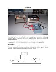
74F74 - Dual D-type flip-flop
74F74 - Dual D-type flip-flop
74F74 - Dual D-type flip-flop

Create successful ePaper yourself
Turn your PDF publications into a flip-book with our unique Google optimized e-Paper software.
Philips Semiconductors<br />
Product specification<br />
<strong>Dual</strong> D-<strong>type</strong> <strong>flip</strong>-<strong>flop</strong><br />
<strong>74F74</strong><br />
FEATURE<br />
• Industrial temperature range available (–40°C to +85°C)<br />
DESCRIPTION<br />
The <strong>74F74</strong> is a dual positive edge-triggered D-<strong>type</strong> <strong>flip</strong>-<strong>flop</strong> featuring<br />
individual data, clock, set, and reset inputs; also true and<br />
complementary outputs. Set (SD) and reset (RD) are asynchronous<br />
active low inputs and operate independently of the clock input. When<br />
set and reset are inactive (high), data at the D input is transferred to<br />
the Q and Q outputs on the low-to-high transition of the clock. Data<br />
must be stable just one setup time prior to the low-to-high transition of<br />
the clock for predictable operation. Clock triggering occurs at a<br />
voltage level and is not directly related to the transition time of the<br />
positive-going pulse. Following the hold time interval, data at the D<br />
input may be changed without affecting the levels of the output.<br />
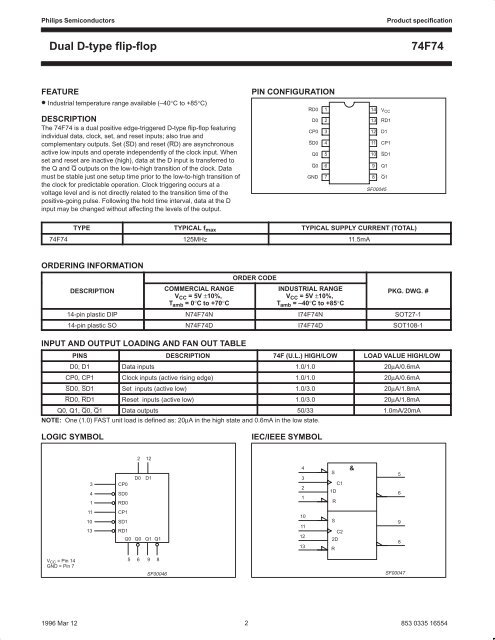
PIN CONFIGURATION<br />
RD0 1<br />
D0 2<br />
CP0 3<br />
SD0 4<br />
Q0 5<br />
Q0 6<br />
GND 7<br />
14 V CC<br />
13 RD1<br />
12 D1<br />
11 CP1<br />
10 SD1<br />
9 Q1<br />
8 Q1<br />
SF00045<br />
TYPE TYPICAL f max TYPICAL SUPPLY CURRENT (TOTAL)<br />
<strong>74F74</strong> 125MHz 11.5mA<br />
ORDERING INFORMATION<br />
DESCRIPTION<br />
COMMERCIAL RANGE<br />
V CC = 5V ±10%,<br />
T amb = 0°C to +70°C<br />
ORDER CODE<br />
INDUSTRIAL RANGE<br />
V CC = 5V ±10%,<br />
T amb = –40°C to +85°C<br />
PKG. DWG. #<br />
14-pin plastic DIP N<strong>74F74</strong>N I<strong>74F74</strong>N SOT27-1<br />
14-pin plastic SO N<strong>74F74</strong>D I<strong>74F74</strong>D SOT108-1<br />
INPUT AND OUTPUT LOADING AND FAN OUT TABLE<br />
PINS DESCRIPTION 74F (U.L.) HIGH/LOW LOAD VALUE HIGH/LOW<br />
D0, D1 Data inputs 1.0/1.0 20µA/0.6mA<br />
CP0, CP1 Clock inputs (active rising edge) 1.0/1.0 20µA/0.6mA<br />
SD0, SD1 Set inputs (active low) 1.0/3.0 20µA/1.8mA<br />
RD0, RD1 Reset inputs (active low) 1.0/3.0 20µA/1.8mA<br />
Q0, Q1, Q0, Q1 Data outputs 50/33 1.0mA/20mA<br />
NOTE: One (1.0) FAST unit load is defined as: 20µA in the high state and 0.6mA in the low state.<br />
LOGIC SYMBOL<br />
IEC/IEEE SYMBOL<br />
2 12<br />
3<br />
4<br />
1<br />
CP0<br />
SD0<br />
RD0<br />
D0<br />
D1<br />
4<br />
3<br />
2<br />
1<br />
S<br />
C1<br />
1D<br />
R<br />
&<br />
5<br />
6<br />
11<br />
10<br />
13<br />
CP1<br />
SD1<br />
RD1<br />
Q0 Q0<br />
Q1 Q1<br />
10<br />
11<br />
12<br />
13<br />
S<br />
C2<br />
2D<br />
R<br />
9<br />
8<br />
V CC = Pin 14<br />
GND = Pin 7<br />
5 6 9 8<br />
SF00046<br />
SF00047<br />
1996 Mar 12 2<br />
853 0335 16554


![More Effective C++ [Meyers96]](https://img.yumpu.com/25323611/1/184x260/more-effective-c-meyers96.jpg?quality=85)