PVDF Phased-Array Analog Front End
PVDF Phased-Array Analog Front End
PVDF Phased-Array Analog Front End

Create successful ePaper yourself
Turn your PDF publications into a flip-book with our unique Google optimized e-Paper software.
F EATURE<br />
ARTICLE<br />
by Matt Oppenheim (United Kingdom)<br />
<strong>PVDF</strong> <strong>Phased</strong>-<strong>Array</strong> <strong>Analog</strong> <strong>Front</strong> <strong>End</strong><br />
Need a board to test algorithms for CDMA signal transmission and processing?<br />
You can employ an array of broadband receivers using thin polyvinylidene<br />
fluoride (<strong>PVDF</strong>) sheets as the transducers. Here you learn about the analog<br />
electronics required to condition the analog signals for digitization and the<br />
subsequent transmission line implementation.<br />
November 2010 – Issue 244<br />
My supervisor appeared at the lab door pulling a<br />
large trolley. “This is the single-channel confabulator<br />
I made for my PhD,” he beamed, showering a pile of<br />
valves, wires, and dust onto the floor. “Make it portable, battery-powered,<br />
and scale it up to eight channels,” he instructed,<br />
disappearing behind the growing mound of antiquated<br />
technology. As he disappeared he muttered: “It’s summer<br />
vacation, so I’m off for three months. Have fun!”<br />
In this article, I present an implementation of an array of<br />
broadband acoustic receivers using thin polyvinylidene fluoride<br />
(<strong>PVDF</strong>) sheets as the transducers. The board is intended<br />
for testing algorithms used in code division multiple access<br />
(CDMA) signal transmission and processing. The final board<br />
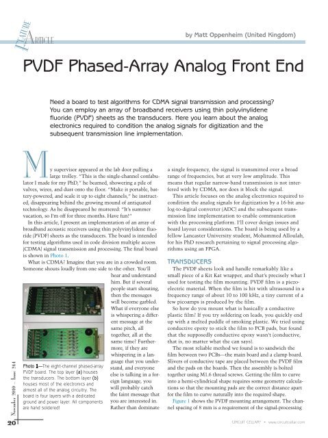
is shown in Photo 1.<br />
What is CDMA? Imagine that you are in a crowded room.<br />
Someone shouts loudly from one side to the other. You’ll<br />
hear and understand<br />
him. But if several<br />
a)<br />
b)<br />
Photo 1—The eight-channel phased-array<br />
<strong>PVDF</strong> board. The top layer (a) houses<br />
the transducers. The bottom layer (b)<br />
houses most of the electronics and<br />
almost all of the analog circuitry. The<br />
board is four layers with a dedicated<br />
ground and power layer. All components<br />
are hand soldered!<br />
people start shouting,<br />
then the messages<br />
will become garbled.<br />
What if everyone else<br />
is whispering a different<br />
message at the<br />
same pitch, all<br />
together, all at the<br />
same time? Furthermore,<br />
if they are<br />
whispering in a language<br />
that you understand,<br />
and everyone<br />
else is talking in a foreign<br />
language, you<br />
will probably catch<br />
the faint message that<br />
you are interested in.<br />
Rather than dominate<br />
a single frequency, the signal is transmitted over a broad<br />
range of frequencies, but at very low amplitude. This<br />
means that regular narrow-band transmission is not interfered<br />
with by CDMA, nor does it block the signal.<br />
This article focuses on the analog electronics required to<br />
condition the analog signals for digitization by a 16-bit analog-to-digital<br />
converter (ADC) and the subsequent transmission<br />
line implementation to enable communication<br />
with the processing platform. I’ll cover design issues and<br />
board layout considerations. The board is being used by a<br />
fellow Lancaster University student, Mohammed Alloulah,<br />
for his PhD research pertaining to signal processing algorithms<br />
using an FPGA.<br />
TRANSDUCERS<br />
The <strong>PVDF</strong> sheets look and handle remarkably like a<br />
small piece of a Kit Kat wrapper, and that’s precisely what I<br />
used for testing the film mounting. <strong>PVDF</strong> film is a piezoelectric<br />
material. When the film is hit with ultrasound in a<br />
frequency range of about 10 to 100 kHz, a tiny current of a<br />
few picoamps is produced by the film.<br />
So how do you mount what is basically a conductive<br />
plastic film? If you try soldering on leads, you quickly end<br />
up with a melted puddle of smoking plastic. We tried using<br />
conductive epoxy to stick the film to PCB pads, but found<br />
that the supposedly conductive epoxy wasn’t (conductive,<br />
that is, no matter what the can says).<br />
The most reliable method we found is to sandwich the<br />
film between two PCBs—the main board and a clamp board.<br />
Slivers of conductive tape are placed between the <strong>PVDF</strong> film<br />
and the pads on the boards. Then the assembly is bolted<br />
together using M1.6 thread screws. Getting the film to curve<br />
into a hemi-cylindrical shape requires some geometry calculations<br />
so that the mounting pads are the correct distance apart<br />
for the film to curve naturally into the required shape.<br />
Figure 1 shows the <strong>PVDF</strong> mounting arrangement. The channel<br />
spacing of 8 mm is a requirement of the signal-processing<br />
20 CIRCUIT CELLAR ® • www.circuitcellar.com
PCB <strong>PVDF</strong> Film Screw<br />
Conductive tape<br />
sandwich<br />
Figure 1—This is the <strong>PVDF</strong> mounting arrangement. [1] (Source: Mike<br />
Hazas)<br />
algorithms implemented on the FPGA board that processes<br />
the final signals produced by the receiver board. These algorithms<br />
are beyond the scope of this article. The clamp PCBs<br />
are attached using two bolts, because with only one bolt they<br />
are free to rotate out of position.<br />
ANALOG SIGNAL CONDITIONING<br />
As you would expect, when the transducer produces a current,<br />
the first stage of the signal-conditioning chain is a current-to-voltage<br />
converter. With such a tiny current to amplify,<br />
the input current offset and bias of the op-amp are critical.<br />
I settled on the OPA129UB manufactured by Texas Instruments,<br />
which is billed as “ultra-low bias current.” This is<br />
quoted as ±30 fA! The noise figure of any amplification chain<br />
depends critically on the first stage, so I used the best part<br />
that I could find.<br />
Nut<br />
You will notice the “T” arrangement of resistors in Figure 2<br />
around the current-to-voltage converter. This allows much<br />
lower values of resistors to be used compared with using a<br />
single resistor. I needed the equivalent of at least a gigaohm<br />
and wanted to be able to try higher values. The disadvantage<br />
of this arrangement (nothing is free!) is that the offset voltage<br />
is amplified by the same factor by which you are reducing the<br />
equivalent single resistor. So long as this offset does not<br />
cause the output signal to approach the voltage rails, this is<br />
not a problem as the output voltage signal from the converter<br />
is decoupled through a capacitor, which eliminates the offset.<br />
To give your tiny signal the best chance of survival, the<br />
layout of components and tracks for the input to this op-amp<br />
are critical. The pinout for the OPA129UB is optimized to<br />
allow for placing guard traces around the inputs. These guard<br />
traces are connected to the “substrate” pin of the amplifier at<br />
a single point, which is grounded. Normally, just having a<br />
ground plane under the traces is considered sufficient to<br />
guard the input lines from interference, but as the input signals<br />
are so tiny, I implemented the whole “belt and braces”<br />
approach of guard traces and ground plane. The guard traces<br />
are connected to the ground plane as close to each end of the<br />
traces as practical.<br />
Next, the signal is filtered to remove unwanted high frequencies.<br />
Phase information is critical for the final signal processing.<br />
So a Bessel filter is used since this does not alter the<br />
Figure 2—A schematic for a single channel, showing the analog signal path<br />
from the transducer to the ADC. The initial current signal is converted to a<br />
voltage and then filtered and amplified.<br />
www.circuitcellar.com • CIRCUIT CELLAR ® 21<br />
November 2010 – Issue 244
a)<br />
b)<br />
reduces the component count compared to noninverting. With<br />
the noninverting configuration, the input needs to be tied to<br />
ground using a resistor; otherwise, the output can have a large<br />
voltage offset. To further eliminate the possibility of DC offset,<br />
I coupled the stages using a capacitor. I may seem a little paranoid,<br />
but what is an extra capacitor between friends? Having<br />
the capacitor between each stage also allows for the subsequent<br />
stages to be easily isolated during debugging: simply lift the<br />
capacitor with some desoldering tweezers (in the unlikely event<br />
that the circuit does not perform flawlessly first time).<br />
Photo 2a shows the amplified and filtered output from the<br />
final op-amp stage and the output from the first op-amp—the<br />
current-to-voltage converter. Note that the amplitude scales<br />
differ by a factor of 100. The signals generated from the currentto-voltage<br />
converter are tiny! As can be seen, the op-amp<br />
amplification and filtering cleans up the signal nicely. The test<br />
signal was generated using a 40-kHz piezoelectric transducer<br />
connected to a function generator.<br />
November 2010 – Issue 244<br />
c)<br />
Photo 2—Oscilloscope screen grabs. a—Here you see the test signal<br />
after amplification and filtering with the signal immediately after<br />
the current-to-voltage conversion. b—This is SPI data from one of<br />
the ADCs alongside the SPI clock. c—These are SPI control signals<br />
(SDI, !CS, bottom !CON).<br />
phase across the bandwidth of the signal. This is implemented<br />
using two Linear Technology LTC2050HV op-amps<br />
(AMP2A and AMP3A in Figure 2). Throughout the design, I<br />
used single op-amp packages for two reasons. The first was<br />
that there is a potential for cross-feed between the op-amp<br />
stages in a multiple package. The second was layout space<br />
restrictions. I needed each stage to fit into the 8-mm spacing<br />
of the <strong>PVDF</strong> films, which made for some tight routing! Still,<br />
it all worked out in the end. I used precision resistors<br />
throughout the filters to maintain consistent characteristics<br />
across the separate channels.<br />
After the filtering are two stages of amplification (AMP5A<br />
and AMP6A in Figure 2). The original design had a single stage.<br />
Initial testing indicated that to get good signal amplitude for<br />
the following stages, the single stage might approach the gainpass<br />
bandwidth limits of the op-amp. I could have stuck with a<br />
single stage and found an op-amp with a higher gain bandwidth,<br />
but I settled on staying with the op-amps I knew and<br />
having two stages of gain instead. It was a tradeoff, as it is<br />
always best to reduce the component count in a design to save<br />
space, power, and cost.<br />
I used the classic inverting amplifier configuration since this<br />
ANALOG-TO-DIGITAL CONVERSION<br />
To provide further attenuation for out-of-band frequencies<br />
and to ensure that no aliasing occurs, a Linear Technology<br />
LTC1569 filter chip is configured as a low-pass filter. This is a<br />
versatile tenth-order filter chip in an eight-pin package. The<br />
filter cutoff frequency is set using a single external resistor.<br />
Refer to the datasheet for details. Linear Technology supplies<br />
its own free FilterCAD software to help you with filter<br />
design. Naturally, the results use their own range of filter<br />
components. C25 in Figure 2 removes the high-frequency<br />
(megahertz range) clock noise from the filter’s output.<br />
The analog-to-digital conversion circuitry was designed by<br />
Mohammed Alloulah in an attempt to limit the damage to<br />
his project because I designed the instrumentation that his<br />
future thesis depends on. A 16-bit Texas Instruments<br />
ADS8329 is used by each channel to convert the conditioned<br />
analog signal to digital. An ADC is only as good as the reference<br />
voltage used to compare your precious signal to, so a<br />
separate voltage-reference IC is used to produce the reference<br />
voltage for each ADC (REF2 in Figure 2). This reference voltage<br />
is further stabilized using a Texas Instruments OPA365<br />
op-amp (AMP7A in Figure 2). This is implemented to overcome<br />
the transient noise that results from the loading effect<br />
taking place during conversion—an inherent effect from the<br />
architecture of the successive-approximation converter.<br />
Details of this layout and configuration were worked out<br />
after spending a lot of time watching a man wearing a cowboy<br />
hat explaining the optimum design and layout configuration<br />
in Texas Instruments’s educational online video series.<br />
Even the type and ESR rating of the capacitors that load the<br />
output from the reference have a measurable effect when<br />
working at 16-bit resolution (C35 in Figure 2). Basically, I<br />
copied their design and component recommendations!<br />
The ADC only draws a small current. Since this is a 3-V<br />
part and the rest of the board uses ±5-V supply rails, a Texas<br />
Instruments REF3133 voltage reference powers each ADC.<br />
This adds a further layer of isolation between the ADC and<br />
the power supply circuitry. The part does not explicitly<br />
require a smoothing capacitor on the VOUT line, but I added<br />
22 CIRCUIT CELLAR ® • www.circuitcellar.com
a)<br />
b)<br />
c)<br />
Photo 3—The transmission cable assembly. a—Take a<br />
look at the shielded ribbon cable and connector components.<br />
b—The connector is ready to press fit. c—I used a<br />
vise to press-fit the connector.<br />
one for extra decoupling.<br />
Photo 2b shows the digital data from<br />
one of the SPI lines. The lower trace<br />
shows a 25-MHz SPI clock signal. Due<br />
to the bandwidth limitation of the<br />
scope, this does not appear as a nice<br />
square wave. Photo 2c shows the other<br />
digital control signals for the ADCs<br />
generated by the FPGA. Because these<br />
are much lower frequency than the<br />
clock line, the scope has the bandwidth<br />
to display them as square waves.<br />
DIGITAL INTERFACE<br />
It’s all analog under the skin! I wanted<br />
as fast an SPI as practical to connect<br />
the receiver board to a Xilinx Virtex II<br />
FPGA development board. Luckily, the<br />
communication science lab is adjacent<br />
to mine, so I was able to consult the<br />
professionals for advice on transmission-line<br />
design. As Robert Lacoste<br />
often mentions in his excellent “The<br />
Darker Side” column, it’s all about<br />
impedance matching. I chose shielded<br />
ribbon cable for the transmission line<br />
as it is relatively straightforward to<br />
work with and butcher (I<br />
use that word accurately)<br />
into connectors. Also, I<br />
could order a single meter of<br />
this cable from my regular<br />
supplier, rather than having<br />
to purchase an entire reel.<br />
Shielded cable is required,<br />
since unshielded cable with<br />
a 25-MHz signal pulsing<br />
along it acts like an antenna.<br />
I don’t think the folks<br />
using the lab’s indoor positioning<br />
systems would<br />
appreciate having to compete<br />
with a homemade<br />
transmitter!<br />
With eight channels of<br />
SPI coming from the board,<br />
and timing control signals<br />
going into it, I needed a lot<br />
of signal lines. Naturally, I<br />
also needed to fit them all<br />
into a small enough footprint<br />
to not require widening<br />
the board since this<br />
would result in having to<br />
rethink the housing.<br />
The 3M MDR range of<br />
connectors seemed suitable<br />
for the job as they have a<br />
small enough footprint for my board<br />
and all of the required genders of connectors<br />
are available from my usual<br />
online supplier. These connectors are<br />
available in both solder cup and insulation<br />
displacement connectors (IDC).<br />
IDC style has the advantage over solder<br />
cups of being much faster to assemble.<br />
Naturally, the manufacturer’s recommended<br />
assembly tool cost a ridiculous<br />
amount of money. After carefully<br />
perusing the assembly instructions, I<br />
figured out a way to press fit all of the<br />
parts together using a vise, a pair of<br />
simple homemade jigs, and copious<br />
amounts of blue tack and insulation<br />
tape. I have put details of this assembly<br />
technique onto my website. Photo 3<br />
shows the cable and connector being<br />
assembled. Photo 4 is the completed<br />
cable and connector. This method<br />
proved to be straightforward and reliable.<br />
I used the lab laser cutter to cut<br />
the 10-mm plastic jigs used to press-fit<br />
the assembly together. As always, no<br />
one was more surprised than I was<br />
when it all worked!<br />
Introducing Pololu’s new<br />
Maestro USB<br />
Servo Controllers<br />
Conduct a<br />
symphony<br />
of servos.<br />
#1350<br />
Micro Maestro<br />
6-Channel<br />
$19.95<br />
#1352<br />
Mini Maestro<br />
12-Channel<br />
$29.95<br />
#1354<br />
Mini Maestro<br />
18-Channel<br />
$39.95<br />
Three control methods: USB, TTL serial,<br />
and internal scripting<br />
Free configuration and control<br />
application with motion sequencer<br />
Channels can be used for digital I/O or<br />
up to 12 analog inputs<br />
Individual servo speed and acceleration<br />
control for each channel<br />
Up to 8 KB of internal scripting memory<br />
(~3000 servo positions)<br />
0.25 us servo pulse resolution with<br />
pulse rate up to 333 Hz<br />
more information at<br />
www.pololu.com/maestro<br />
#1356<br />
Mini Maestro<br />
24-Channel<br />
$49.95<br />
Pololu's 6-channel Micro Maestro and<br />
new 12-, 18-, and 24-channel Mini<br />
Maestros take serial servo controllers to<br />
the next level by incorporating native USB<br />
control for easy connection to a PC and<br />
programmability via a simple scripting<br />
language for self-contained, host<br />
controller-free applications. Whether you<br />
want the best servo controller available or<br />
a versatile, general-purpose I/O control<br />
board, these compact devices will deliver.<br />
www.circuitcellar.com • CIRCUIT CELLAR<br />
®<br />
23<br />
November 2010 – Issue 244
The only disadvantage of my cable<br />
assembly is that the shielded casing is<br />
not available for 50-way flat ribbon<br />
cable. I got around this by modifying<br />
the round cable-shielded casing with<br />
the judicious use of a hacksaw and file.<br />
The type of casing I wanted is made for<br />
just about any other width of cable!<br />
From the datasheet, the characteristic<br />
impedance of the ribbon cable is 50<br />
Ω. Signals originating from the ADC<br />
and going to the FPGA are impedance<br />
matched using a 50-Ω resistor. Signals<br />
coming from the FPGA to the ADC<br />
were terminated using a 50-Ω resistor<br />
in series with a 0.1-µF capacitor. The<br />
theory behind these termination techniques<br />
can be found in Ron Schmitt’s<br />
2002 book titled Electromagnetics<br />
Explained.<br />
To eliminate cross-feed between the<br />
rapidly switching digital lines, I<br />
grounded a wire in between each signal<br />
wire on the ribbon cable. If the signals<br />
were differential, I would have used a<br />
twisted-pair configuration, but SPI signals<br />
are not differential.<br />
I built a board that plugs onto the<br />
Xilinx development board to allow my<br />
cable to connect with the signal pins<br />
on the FPGA. This has impedancematching<br />
resistors for the signals that<br />
originate from the FPGA going to my<br />
Photo 4—The breakout board and DAC<br />
receiver board. Photo 4 shows the<br />
breakout board mounted on the Xilinx<br />
development board. Because all of the<br />
signals on the Xilinx board are digital,<br />
it is not necessary to add external<br />
shielding to this board to protect it<br />
from interference. However, having<br />
digital pins switching quickly acts as a<br />
transmitting antenna, so it would be<br />
necessary to case the board for a commercial<br />
product to comply with emission<br />
standards.<br />
The output characteristics for the SPI<br />
clock line from the FPGA are critical for<br />
the interface to work. As always, read the<br />
datasheet carefully! We had to play around<br />
with the setting for the current limit of<br />
the pin to get life from the SPI bus.<br />
CASING & PCB LAYOUT<br />
I found a range of conductive plastic<br />
cases rated for EMC protection. The big<br />
advantage over using a metal case is the<br />
ease with which they can be machined.<br />
It’s always a good idea to start looking at<br />
cases as early on as practical. The case<br />
dimensions and mounting arrangement<br />
act as major constraints on your PCB<br />
layout and dimensions.<br />
I used CadSoft Computer’s Eagle v5.6<br />
for the schematic capture and PCB layout.<br />
I didn’t touch the autorouter and<br />
don’t advise anyone to do so. I used four<br />
layers with a layer dedicated to ground.<br />
Optimizing the ground return path is<br />
critical to analog design. I did not use<br />
separate analog and digital ground layers.<br />
I used a separate lobe of ground for<br />
each of the analog channels and connected<br />
them to a large unbroken area of<br />
ground under the digital connector using<br />
a neck placed under the ADCs.<br />
I fit each channel into the width of<br />
the <strong>PVDF</strong> film transducer—8 mm. Routing<br />
is 90% component layout. It is a<br />
false economy to start laying down track<br />
until you have every part for the block<br />
that you are working on in an optimum<br />
position. This took some time, but like<br />
many engineers, I find PCB layout<br />
engrossing.<br />
Once I had a single channel completed,<br />
I found a user language program<br />
(ULP) called “duplicate board”<br />
that allows a completed block of layout<br />
November 2010 – Issue 244<br />
Figure 3—The schematic for the lithium battery power board (±5 V)<br />
24 CIRCUIT CELLAR ® • www.circuitcellar.com
to be duplicated with a little fiddling. Look on the Eagle user<br />
group notice board for details.<br />
DAC BOARD<br />
We also designed a daughterboard for the FPGA board that<br />
enables the FPGA to produce an analog signal. This was originally<br />
designed to enable the testing of fancy transmission algorithms<br />
beyond the scope of this article. Here we used it for recreating<br />
the test signals that are received by the receiver board<br />
as a quick check that everything works. Schematics and a<br />
board layout are also included on the Circuit Cellar FTP site.<br />
POWER SUPPLY<br />
Any ripple or noise on the power lines reduces the chances<br />
of maintaining signal resolution through the amplifier and<br />
filter stages and compromise the workable range of the 16-<br />
bit ADC. Rechargeable lithium batteries are chosen as the<br />
power source along with quality Linear Technology linear<br />
regulators to produce the ±5-V power rails. Using batteries<br />
has the strong advantage of producing an output free of highfrequency<br />
ripple.<br />
I added some low-battery-voltage indicators using <strong>Analog</strong><br />
Devices ADCMP361 comparators. These have a built-in<br />
voltage reference. Trying to work out how to hook one up<br />
to the negative supply battery and the –5-V output rail to<br />
indicate when the battery voltage was flagging took a little<br />
figuring!<br />
Capacitance is your friend when it comes to smoothing<br />
the supply lines. Batteries can react in the kilohertz range to<br />
changes in load. Capacitors can react in the megahertz range.<br />
This means that a capacitor attached directly to the supply<br />
pins of each IC provides a little power supply adjacent to the<br />
chip that can react at the same frequency that the chip is<br />
operating at. Extra capacitors adjacent to the power board<br />
connectors on the main board further add to this decoupling<br />
of the battery supply from the instantaneous demands of the<br />
circuitry. At the relatively low frequencies that this board<br />
works, capacitor type and placement is not as critical as<br />
when working at high frequencies.<br />
I initially used some ribbon cable IDC connectors to bring<br />
the power to the main board and doubled up on each pin in<br />
order not to exceed the maximum allowed current draw<br />
through the sockets. Although this particular set of connectors<br />
is excellent for digital signals, I went for a more robust<br />
and larger Tyco 0.1″ IDC connectors on the board revision,<br />
as they have much larger pins, which gives a tighter connection<br />
with a complete overkill of current rating. I checked<br />
that I could obtain the connectors from more than one local<br />
supplier. While you can often drop a replacement amplifier<br />
into a design without having to alter any of the layout, connectors<br />
are a pain to replace as they usually have a unique<br />
footprint. Figure 3 depicts the power supply’s circuitry and<br />
layout.<br />
BOARD SUCCESS<br />
The board successfully amplified, filtered, and digitized the<br />
signals received by all eight transducers. Clamping the foils is<br />
excessively fiddly as it relies on an operator to accurately<br />
place the transducers. A more consistent system of transducer<br />
clamping needs to be found if the device is ever scaled up.<br />
The transmission cable termination method proved affordable<br />
and reliable, showing I do not need to invest in the connector<br />
manufacturer’s expensive crimping tools for low-volume<br />
production. I proved that it is possible to populate and<br />
hand-solder a ridiculously complex board. The cost to my<br />
sanity may have been excessive, though!I<br />
Author’s note: MDR Cable assembly notes are available on my<br />
website: http://sites.google.com/site/hardwaremonkey/home/<br />
cable-assembly. Mohammed Alloulah made a substantial contribution<br />
to this design during his ongoing PhD research on signal<br />
processing, especially with filter design and ADC circuitry. I hope<br />
that the final circuit will contribute to his thesis.<br />
Matt Oppenheim (matt.oppenheim@ gmail.com) holds an MSc in<br />
Mechatronic Systems Engineering from Lancaster University. He<br />
splits his time working offshore as a Chief Geophysicist for Polarcus<br />
onboard seismic survey ships and as a Research Assistant at<br />
InfoLab21, Lancaster University. Matt’s first love is analog technology,<br />
but he can be persuaded to work on digital projects as well.<br />
In his spare time, Matt enjoys cycling and drawing cartoons.<br />
PROJECT FILES<br />
To download the project files, go to ftp://ftp.circuitcellar.<br />
com/pub/Circuit_Cellar/2010/244.<br />
REFERENCE<br />
[1] M. Hazas, “Indoor Location Systems,” PhD Thesis,<br />
Dept. of Engineering, Cambridge University, UK, 2002.<br />
RESOURCES<br />
H. Johnson, “Multiple ADC Grounding,” EDN, 2001.<br />
Linear Technology, “LTC1569-7: Linear Phase, DC<br />
Accurate, Tunable, 10 th Order Lowpass Filter,” 1998.<br />
R. Schmitt, Electromagnetics Explained: A Handbook<br />
for Wireless/RF, EMC, and High-Speed Electronics,<br />
Newnes, 2002.<br />
Texas Instruments, “OPA129 Ultra-Low Bias Current<br />
Difet Operational Amplifier,” SBOS026A, 2007.<br />
SOURCES<br />
ADCMP361 Comparator<br />
<strong>Analog</strong> Devices, Inc. | www.analog.com<br />
Eagle software<br />
CadSoft Computer | www.cadsoftusa.com<br />
LTC1569 Filter and LTC2050HV op-amp<br />
Linear Technology | www.linear.com<br />
ADS8329 ADC, OPA365 op-amp, and REF3133 voltage<br />
reference<br />
Texas Instruments, Inc. | www.ti.com<br />
Virtex-II FPGA Development board<br />
Xilinx | www.xilinx.com<br />
www.circuitcellar.com • CIRCUIT CELLAR ® 25<br />
November 2010 – Issue 244