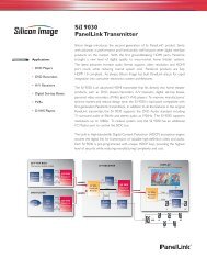
D a t a S h e e t - SemiconductorStore.com
D a t a S h e e t - SemiconductorStore.com
D a t a S h e e t - SemiconductorStore.com

Create successful ePaper yourself
Turn your PDF publications into a flip-book with our unique Google optimized e-Paper software.
8. LAYOUT AND SOLDERING CONSIDERATIONS<br />
8.1 Soldering re<strong>com</strong>mendations<br />
WT12 is <strong>com</strong>patible with industrial standard reflow profile for Pb-free solders. The reflow<br />
profile used is dependent on the thermal mass of the entire populated PCB, heat transfer<br />
efficiency of the oven and particular type of solder paste used. Consult the datasheet of<br />
particular solder paste for profile configurations.<br />
Bluegiga Technologies will give following re<strong>com</strong>mendations for soldering the module to<br />
ensure reliable solder joint and operation of the module after soldering. Since the profile<br />
used is process and layout dependent, the optimum profile should be studied case by case.<br />
Thus following re<strong>com</strong>mendation should be taken as a starting point guide.<br />
• Refer to technical documentations of particular solder paste for profile configurations<br />
• Avoid using more than one flow.<br />
• Reliability of the solder joint and self-alignment of the <strong>com</strong>ponent are dependent on<br />
the solder volume. Minimum of 150μm stencil thickness is re<strong>com</strong>mended.<br />
• Aperture size of the stencil should be 1:1 with the pad size.<br />
• A low residue, “no clean” solder paste should be used due to low mounted height of<br />
the <strong>com</strong>ponent.<br />
8.2 Layout guidelines<br />
It is strongly re<strong>com</strong>mended to use good layout practices to ensure proper operation of the<br />
module. Placing copper or any metal near antenna deteriorates its operation by having<br />
effect on the matching properties. Metal shield around the antenna will prevent the<br />
radiation and thus metal case should not be used with the module. Use grounding vias<br />
separated max 3 mm apart at the edge of grounding areas to prevent RF penetrating<br />
inside the PCB and causing an unintentional resonator. Use GND vias all around the PCB<br />
edges. Figure 5 illustrates re<strong>com</strong>mended PCB design around the antenna of WT12 when<br />
the module is placed at the edge of a PCB.<br />
Do not place copper on the top layer under the module, as shown in figure 5. The module<br />
has vias on the area shown, which can cause short circuit if there is copper underneath.<br />
Any metal placed closer than 20 mm in any direction from the antenna changes the<br />
matching properties and thus will considerably deteriorate the RF performance of the<br />
module.<br />
44