M_TTCAN - User Manual - Bosch Semiconductors and Sensors
M_TTCAN - User Manual - Bosch Semiconductors and Sensors
M_TTCAN - User Manual - Bosch Semiconductors and Sensors

Create successful ePaper yourself
Turn your PDF publications into a flip-book with our unique Google optimized e-Paper software.
M_<strong>TTCAN</strong> Revision 3.0.2<br />
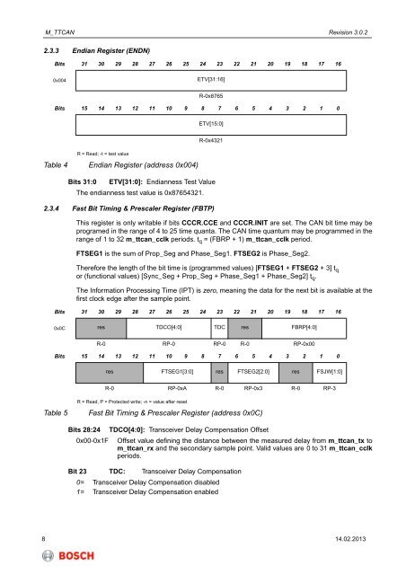
2.3.3 Endian Register (ENDN)<br />
Bits 31 30 29 28 27 26 25 24 23 22 21 20 19 18 17 16<br />
0x004<br />
ETV[31:16]<br />
R-0x8765<br />
Bits 15 14 13 12 11 10 9 8 7 6 5 4 3 2 1 0<br />
ETV[15:0]<br />
R = Read; -t = test value<br />
Table 4 Endian Register (address 0x004)<br />
R-0x4321<br />
Bits 31:0 ETV[31:0]: Endianness Test Value<br />
The endianness test value is 0x87654321.<br />
2.3.4 Fast Bit Timing & Prescaler Register (FBTP)<br />
This register is only writable if bits CCCR.CCE <strong>and</strong> CCCR.INIT are set. The CAN bit time may be<br />
programed in the range of 4 to 25 time quanta. The CAN time quantum may be programmed in the<br />
range of 1 to 32 m_ttcan_cclk periods. t q = (FBRP + 1) m_ttcan_cclk period.<br />
FTSEG1 is the sum of Prop_Seg <strong>and</strong> Phase_Seg1. FTSEG2 is Phase_Seg2.<br />
Therefore the length of the bit time is (programmed values) [FTSEG1 + FTSEG2 +3]t q<br />
or (functional values) [Sync_Seg + Prop_Seg + Phase_Seg1 + Phase_Seg2] t q .<br />
The Information Processing Time (IPT) is zero, meaning the data for the next bit is available at the<br />
first clock edge after the sample point.<br />
Bits 31 30 29 28 27 26 25 24 23 22 21 20 19 18 17 16<br />
0x0C res TDCO[4:0] TDC res FBRP[4:0]<br />
R-0 RP-0 RP-0 R-0 RP-0x00<br />
Bits 15 14 13 12 11 10 9 8 7 6 5 4 3 2 1 0<br />
res FTSEG1[3:0] res FTSEG2[2:0] res FSJW[1:0]<br />
R-0 RP-0xA R-0 RP-0x3 R-0 RP-3<br />
Table 5<br />
R = Read, P = Protected write; -n = value after reset<br />
Fast Bit Timing & Prescaler Register (address 0x0C)<br />
Bits 28:24 TDCO[4:0]: Transceiver Delay Compensation Offset<br />
0x00-0x1F Offset value defining the distance between the measured delay from m_ttcan_tx to<br />
m_ttcan_rx <strong>and</strong> the secondary sample point. Valid values are 0 to 31 m_ttcan_cclk<br />
periods.<br />
Bit 23 TDC: Transceiver Delay Compensation<br />
0= Transceiver Delay Compensation disabled<br />
1= Transceiver Delay Compensation enabled<br />
8 14.02.2013