SIPMOS Small-Signal Transistor BSP 135 - Menno van der Veen
SIPMOS Small-Signal Transistor BSP 135 - Menno van der Veen
SIPMOS Small-Signal Transistor BSP 135 - Menno van der Veen

You also want an ePaper? Increase the reach of your titles
YUMPU automatically turns print PDFs into web optimized ePapers that Google loves.
<strong>SIPMOS</strong> ® <strong>Small</strong>-<strong>Signal</strong> <strong>Transistor</strong> <strong>BSP</strong> <strong>135</strong><br />
● V DS 600 V<br />
● I D 0.100 A<br />
● R DS(on) 60 Ω<br />
● N channel<br />
● Depletion mode<br />
● High dynamic resistance<br />
● Available grouped in V GS(th)<br />
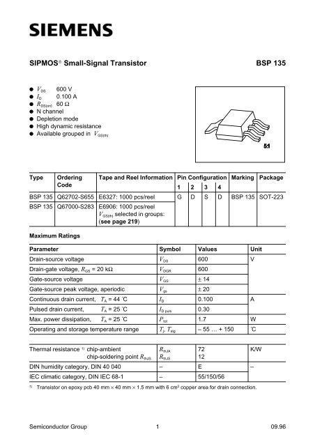
Type Or<strong>der</strong>ing Tape and Reel Information Pin Configuration Marking Package<br />
Code<br />
1 2 3 4<br />
<strong>BSP</strong> <strong>135</strong> Q62702-S655 E6327: 1000 pcs/reel G D S D <strong>BSP</strong> <strong>135</strong> SOT-223<br />
<strong>BSP</strong> <strong>135</strong> Q67000-S283 E6906: 1000 pcs/reel<br />
V GS(th) selected in groups:<br />
(see page 219)<br />
Maximum Ratings<br />
Parameter Symbol Values Unit<br />
Drain-source voltage V DS 600 V<br />
Drain-gate voltage, R GS = 20 kΩ V DGR 600<br />
Gate-source voltage V GS ± 14<br />
Gate-source peak voltage, aperiodic V gs ± 20<br />
Continuous drain current, T A = 44 ˚C I D 0.100 A<br />
Pulsed drain current, T A = 25 ˚C I D puls 0.30<br />
Max. power dissipation, T A = 25 ˚C P tot 1.7 W<br />
Operating and storage temperature range T j , T stg – 55 … + 150 ˚C<br />
Thermal resistance 1)<br />
chip-ambient<br />
chip-sol<strong>der</strong>ing point R thJS<br />
R thJA 72<br />
R thJS 12<br />
DIN humidity category, DIN 40 040 – E –<br />
IEC climatic category, DIN IEC 68-1 – 55/150/56<br />
1)<br />
<strong>Transistor</strong> on epoxy pcb 40 mm × 40 mm × 1.5 mm with 6 cm 2 copper area for drain connection.<br />
K/W<br />
Semiconductor Group 1 09.96
<strong>BSP</strong> <strong>135</strong><br />
Electrical Characteristics<br />
at T j = 25 ˚C, unless otherwise specified.<br />
Parameter Symbol Values Unit<br />
min. typ. max.<br />
Static Characteristics<br />
Drain-source breakdown voltage<br />
V GS = − 3 V, I D = 0.25 mA<br />
Gate threshold voltage<br />
V DS = 3 V, I D = 1 mA<br />
Drain-source cutoff current<br />
V DS = 600 V, V GS = − 3 V<br />
T j = 25 ˚C<br />
T j = 125 ˚C<br />
Gate-source leakage current<br />
V GS = 20 V, V DS = 0<br />
Drain-source on-resistance<br />
V GS = 0 V, I D = 0.01 A<br />
V (BR)DSS<br />
600 – –<br />
V GS(th)<br />
− 1.8 − 1.5 − 0.7<br />
–<br />
–<br />
–<br />
–<br />
100<br />
200<br />
I GSS<br />
– 10 100<br />
R DS(on)<br />
– 40 60<br />
V<br />
nA<br />
µA<br />
nA<br />
Ω<br />
g<br />
Dynamic Characteristics<br />
Forward transconductance<br />
S<br />
V DS ≥ 2 × I D × R DS(on)max , I D = 0.01 A<br />
fs<br />
0.01 0.04 –<br />
Input capacitance<br />
C iss<br />
pF<br />
V GS = − 3 V, V DS = 25 V, f = 1 MHz<br />
– 110 150<br />
Output capacitance<br />
V GS = − 3 V, V DS = 25 V, f = 1 MHz<br />
C oss<br />
– 8 12<br />
Reverse transfer capacitance<br />
V GS = − 3 V, V DS = 25 V, f = 1 MHz<br />
C rss<br />
– 3 5<br />
Turn-on time t on , (t on = t d(on) + t r ) t d(on) – 4 6 ns<br />
V DD =30V,V GS = − 3 V ... + 5 V, R GS =50Ω, t r – 10 15<br />
I D = 0.2 A<br />
Turn-off time t off , (t off = t d(off) + t f ) t d(off) – 15 20<br />
V DD =30V,V GS = − 3 V ... + 5 V, R GS =50Ω,<br />
I D = 0.2 A<br />
t f – 20 30<br />
Semiconductor Group 2
<strong>BSP</strong> <strong>135</strong><br />
Electrical Characteristics (cont’d)<br />
at T j = 25 ˚C, unless otherwise specified.<br />
Parameter Symbol Values Unit<br />
Reverse Diode<br />
Continuous reverse drain current<br />
T A = 25 ˚C<br />
Pulsed reverse drain current<br />
T A = 25 ˚C<br />
Diode forward on-voltage<br />
I F = 0.2 A, V GS = 0<br />
min. typ. max.<br />
I S<br />
– – 0.100<br />
I SM<br />
– – 0.300<br />
V SD<br />
– 0.90 1.30<br />
A<br />
V<br />
V GS(th) Grouping Symbol Limit Values Unit Test Condition<br />
min. max.<br />
Range of V GS(th) ∆V GS(th) – 0.15 V –<br />
Threshold voltage selected in groups 1) :<br />
P<br />
R<br />
S<br />
T<br />
U<br />
V<br />
W<br />
1) A specific group cannot be or<strong>der</strong>ed separately.<br />
Each reel only contains transistors from one group.<br />
Package Outline<br />
V GS(th)<br />
– 0.95<br />
– 1.08<br />
– 1.21<br />
– 1.34<br />
– 1.47<br />
– 1.60<br />
– 1.73<br />
– 0.80<br />
– 0.93<br />
– 1.06<br />
– 1.19<br />
– 1.32<br />
– 1.45<br />
– 1.58<br />
V<br />
V<br />
V<br />
V<br />
V<br />
V<br />
V<br />
V DS1 = 0.2 V;<br />
V DS2 = 3 V;<br />
I D = 1 mA<br />
SOT-223<br />
Dimensions in mm<br />
Semiconductor Group 3
Characteristics<br />
at T j = 25 ˚C, unless otherwise specified<br />
Total power dissipation P tot = f (T A )<br />
Typ. output characteristics I D = f (V DS )<br />
parameter: t p = 80 µs<br />
<strong>BSP</strong> <strong>135</strong><br />
Safe operating area I D = f (V DS )<br />
parameter: D = 0.01, T C = 25 ˚C<br />
Typ. drain-source on-resistance<br />
R DS(on) = f (I D )<br />
parameter: V GS<br />
Semiconductor Group 4
<strong>BSP</strong> <strong>135</strong><br />
Typ. transfer characteristics I D = f (V GS )<br />
parameter: t p = 80 µs, V DS ≥ 2 × I D × R DS(on)max.<br />
Typ. forward transconductance g fs = f (I D )<br />
parameter: V DS ≥ 2 × I D × R DS(on)max. , t p = 80 µs<br />
Drain-source on-resistance<br />
R DS(on) = f(T j )<br />
parameter: I D = 0.01 A, V GS = 0 V, (spread)<br />
Typ. capacitances C = f (V DS )<br />
parameter: V GS = 0, f = 1 MHz<br />
Semiconductor Group 5
<strong>BSP</strong> <strong>135</strong><br />
Gate threshold voltage V GS(th) = f (T j )<br />
parameter: V DS = 3 V, I D = 1 mA, (spread)<br />
Forward characteristics of reverse diode<br />
I F = f (V SD )<br />
parameter: t p = 80 µs, T j , (spread)<br />
Drain current I D = f (T A )<br />
parameter: V GS ≥ 3 V<br />
Transient thermal impedance Z thJA = f (t p )<br />
parameter: D = t p / T<br />
Semiconductor Group 6
<strong>BSP</strong> <strong>135</strong><br />
Drain-source breakdown voltage<br />
V (BR) DSS = b × V (BR)DSS (25 ˚C)<br />
Safe operating area I D = f (V DS )<br />
parameter: D = 0, T C = 25 ˚C<br />
Semiconductor Group 7
This datasheet has been download from:<br />
www.datasheetcatalog.com<br />
Datasheets for electronics components.