ieee transactions on very large scale integration (vlsi) - Computer ...
ieee transactions on very large scale integration (vlsi) - Computer ...
ieee transactions on very large scale integration (vlsi) - Computer ...

You also want an ePaper? Increase the reach of your titles
YUMPU automatically turns print PDFs into web optimized ePapers that Google loves.
IEEE TRANSACTIONS ON VERY LARGE SCALE INTEGRATION (VLSI) SYSTEMS, VOL. 14, NO. 7, JULY 2006 763<br />
Extracti<strong>on</strong> Error Modeling and Automated Model<br />
Debugging in High-Performance Custom Designs<br />
Yu-Shen Yang, Student Member, IEEE, Andreas Veneris, Senior Member, IEEE, Paul Thadikaran, Member, IEEE,<br />
and Srikanth Venkataraman, Member, IEEE<br />
Abstract—In the design cycle of high-performance integrated<br />
circuits, it is comm<strong>on</strong> that certain comp<strong>on</strong>ents are designed directly<br />
at the transistor level. This level of design representati<strong>on</strong><br />
may not be appropriate for test generati<strong>on</strong> tools that usually<br />
require a model expressed at the gate level. Logic extracti<strong>on</strong> is a<br />
key step in test model generati<strong>on</strong> to produce a gate-level netlist<br />
from the transistor-level representati<strong>on</strong>. This is a semi-automated<br />
process which is error-pr<strong>on</strong>e. Once a test model is found to be<br />
err<strong>on</strong>eous, manual debugging is required, which is a resourceintensive<br />
and time-c<strong>on</strong>suming process. This paper presents an<br />
in-depth analysis of typical sets of extracti<strong>on</strong> errors found in the<br />
test model representati<strong>on</strong>s of the pipelines in high-performance<br />
designs today. It also develops an automated debugging soluti<strong>on</strong><br />
for single extracti<strong>on</strong> errors for pipelines with no state equivalence<br />
informati<strong>on</strong>. A suite of experiments <strong>on</strong> circuits with similar architecture<br />
to that found in the industry c<strong>on</strong>firms the fitness and<br />
practicality of the soluti<strong>on</strong>.<br />
Index Terms—Debugging, errors, extracti<strong>on</strong>, test model, VLSI.<br />
I. INTRODUCTION<br />
LARGE AND complex VLSI designs such as microprocessors,<br />
systems-<strong>on</strong>-chip (SoCs), and applicati<strong>on</strong> specific<br />
integrated circuits (ASICs) often require high-performance<br />
low-power custom logic blocks designed at the transistor level<br />
[2], [3], [5], [12], [17], [21], [22]. Since a transistor-level representati<strong>on</strong><br />
cannot be used directly to generate producti<strong>on</strong> tests, a<br />
gate (logic)-level representati<strong>on</strong> of these blocks, also known as<br />
a test model, is extracted from the transistor schematic and used<br />
instead. Logic extracti<strong>on</strong> is a semi-automated process which is<br />
error-pr<strong>on</strong>e [16], [21], [22]. Since the amount of verificati<strong>on</strong> <strong>on</strong><br />
the test model before test generati<strong>on</strong> can be limited, extracti<strong>on</strong> errors<br />
may carry forward in test generati<strong>on</strong> and discovered during<br />
test validati<strong>on</strong>. At that point, manual debugging is performed,<br />
which is a time-c<strong>on</strong>suming and resource-intensive process.<br />
Traditi<strong>on</strong>ally, generati<strong>on</strong> of scan tests for high-volume<br />
manufacturing of complex VLSI circuits with custom-made<br />
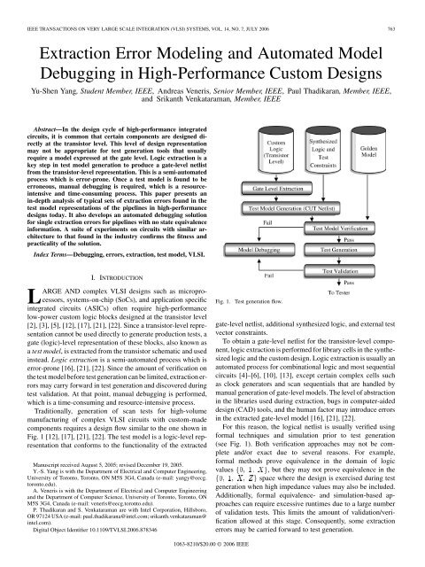
comp<strong>on</strong>ents requires a design flow similar to the <strong>on</strong>e shown in<br />
Fig. 1 [12], [17], [21], [22]. The test model is a logic-level representati<strong>on</strong><br />
that c<strong>on</strong>forms to the functi<strong>on</strong>ality of the extracted<br />
Manuscript received August 5, 2005; revised December 19, 2005.<br />
Y.-S. Yang is with the Department of Electrical and <strong>Computer</strong> Engineering,<br />
University of Tor<strong>on</strong>to, Tor<strong>on</strong>to, ON M5S 3G4, Canada (e-mail: yangy@eecg.<br />
tor<strong>on</strong>to.edu).<br />
A. Veneris is with the Department of Electrical and <strong>Computer</strong> Engineering<br />
and the Department of <strong>Computer</strong> Science, University of Tor<strong>on</strong>to, Tor<strong>on</strong>to, ON<br />
M5S 3G4, Canada (e-mail: veneris@eecg.tor<strong>on</strong>to.edu).<br />
P. Thadikaran and S. Venkataraman are with Intel Corporati<strong>on</strong>, Hillsboro,<br />
OR 97124 USA (e-mail: paul.thadikarana@intel.com; srikanth.venkataraman@<br />
intel.com).<br />
Digital Object Identifier 10.1109/TVLSI.2006.878346<br />
Fig. 1. Test generati<strong>on</strong> flow.<br />
gate-level netlist, additi<strong>on</strong>al synthesized logic, and external test<br />
vector c<strong>on</strong>straints.<br />
To obtain a gate-level netlist for the transistor-level comp<strong>on</strong>ent,<br />
logic extracti<strong>on</strong> is performed for library cells in the synthesized<br />
logic and the custom design. Logic extracti<strong>on</strong> is usually an<br />
automated process for combinati<strong>on</strong>al logic and most sequential<br />
circuits [4]–[6], [10], [13], except certain complex cells such<br />
as clock generators and scan sequentials that are handled by<br />
manual generati<strong>on</strong> of gate-level models. The level of abstracti<strong>on</strong><br />
in the libraries used during extracti<strong>on</strong>, bugs in computer-aided<br />
design (CAD) tools, and the human factor may introduce errors<br />
in the extracted gate-level model [16], [21], [22].<br />
For this reas<strong>on</strong>, the logical netlist is usually verified using<br />
formal techniques and simulati<strong>on</strong> prior to test generati<strong>on</strong><br />
(see Fig. 1). Both verificati<strong>on</strong> approaches may not be complete<br />
and/or exact due to several reas<strong>on</strong>s. For example,<br />
formal methods prove equivalence in the domain of logic<br />
values<br />
, but they may not prove equivalence in the<br />
space where the design is exercised during test<br />
generati<strong>on</strong> when high impedance values may also be included.<br />
Additi<strong>on</strong>ally, formal equivalence- and simulati<strong>on</strong>-based approaches<br />
can require excessive runtimes due to a <strong>large</strong> number<br />
of validati<strong>on</strong> tests. This limits the amount of validati<strong>on</strong>/verificati<strong>on</strong><br />
allowed at this stage. C<strong>on</strong>sequently, some extracti<strong>on</strong><br />
errors may be carried forward to test generati<strong>on</strong>.<br />
1063-8210/$20.00 © 2006 IEEE
764 IEEE TRANSACTIONS ON VERY LARGE SCALE INTEGRATION (VLSI) SYSTEMS, VOL. 14, NO. 7, JULY 2006<br />
Following test generati<strong>on</strong>, the generated tests are again verified<br />
against the golden model to ensure test correctness, which<br />
is a process known as test (vector) validati<strong>on</strong>. Tests may fail in<br />
this step due to errors introduced in model generati<strong>on</strong> but not<br />
identified during model verificati<strong>on</strong>. When the test model fails,<br />
whether this is during verificati<strong>on</strong> or afterwards during test validati<strong>on</strong>,<br />
manual analysis of the failures is the current industrial<br />
practice, also shown in Fig. 1. This is a daunting task for the test<br />
engineer that may delay test deli<strong>very</strong> to the factories and/or may<br />
reduce their quality.<br />
In this study, we describe a set of extracti<strong>on</strong> errors that<br />
are typical in test model generati<strong>on</strong> for the pipeline comp<strong>on</strong>ent(s)<br />
of high-performance designs that have high frequencies<br />
GHz , c<strong>on</strong>sume little power, and meet strict reliability and<br />
performance c<strong>on</strong>straints [2], [3], [7], [8], [11]. Such errors may<br />
occur because of err<strong>on</strong>eous module mapping during extracti<strong>on</strong><br />
and because of library specificati<strong>on</strong> inaccuracies when complex<br />
hardware such as memory elements, multiple clock domains,<br />
and tri-state devices are integrated together. The manual interference<br />
of the designer/test engineer with the design may also<br />
introduce errors.<br />
We also develop an automated simulati<strong>on</strong>-based debugging<br />
soluti<strong>on</strong> that handles single extracti<strong>on</strong> errors in the pipeline of<br />
test models. The proposed soluti<strong>on</strong> does not assume that there<br />
is any corresp<strong>on</strong>dence of primitives between the transistor-level<br />
schematic and the test model. It also works <strong>on</strong> extracted gatelevel<br />
descripti<strong>on</strong>s with no (and/or partial) state equivalence informati<strong>on</strong><br />
to the transistor-level representati<strong>on</strong>. Lack of state/<br />
primitive equivalence informati<strong>on</strong> between the test model and<br />
the transistor-level schematic increases the problem complexity<br />
and the debugging effort by the designer. It should be noted that<br />
the nature and the effects of extracti<strong>on</strong> errors are radically different<br />
from the well-examined topic of design errors presented<br />
in [1]. For example, unlike the error types described here, the<br />
error model proposed by Abadir et al. [1] does not include primitives<br />
such as flip-flops and tri-state devices, and it does not<br />
apply to functi<strong>on</strong>al errors that arise from err<strong>on</strong>eous timing of the<br />
circuit. Therefore, design-error debugging techniques [18], [19]<br />
may not be applicable/efficient when applied to this problem.<br />
An extensive suite of experiments <strong>on</strong> designs with similar architecture<br />
to that found in industry dem<strong>on</strong>strates the practicality<br />
of the approach. Methods such as the <strong>on</strong>e presented here benefit<br />
the testing of microprocessors, ASICs, and SoCs. They help<br />
in identifying model inaccuracies at early stages of the design<br />
cycle, reducing test deli<strong>very</strong> turnaround time and improving test<br />
model generati<strong>on</strong>.<br />
The remaining paper is structured as follows. Secti<strong>on</strong> II<br />
presents the circuit architecture and gives more details about the<br />
intricacies of the particular problem. Secti<strong>on</strong> III c<strong>on</strong>tains a study<br />
of different types of extracti<strong>on</strong> errors that are typical in a modern<br />
industrial envir<strong>on</strong>ment for high-performance integrated circuits.<br />
Secti<strong>on</strong> IV describes the debugging methodology, and Secti<strong>on</strong> V<br />
presents the experiments. Secti<strong>on</strong> VI c<strong>on</strong>cludes this work.<br />
II. PRELIMINARIES<br />
Extracti<strong>on</strong> builds a logic representati<strong>on</strong>, known as the test<br />
model, from a custom transistor-level block [4]–[6], [10], [13].<br />
This representati<strong>on</strong> is later used for test generati<strong>on</strong>. This work<br />
Fig. 2. Benchmark architecture.<br />
assumes that the extracted netlist c<strong>on</strong>tains , , ,<br />
and - buffer and flip-flop primitives. For simplicity,<br />
we assume that the reset event for all flip-flop memory elements<br />
with a reset line is positive-edge-triggered [15]. Flipflops<br />
with level-sensitive reset are not implemented, but the proposed<br />
debugging algorithm is not affected, as explained later<br />
in the paper. Circuits are simulated under a five-logic value set<br />
, where logic represents the unknown<br />
value and denotes a different type of unknown value utilized<br />
in debugging. A logic represents a high-impedance state<br />
- devices generati<strong>on</strong>. However, for simulati<strong>on</strong> purposes,<br />
a logic is replaced with an unknown . For example,<br />
if a - buffer feeds a gate, the output of that gate<br />
will be an unknown .<br />
In implementati<strong>on</strong>, a zero delay simulator is used for all<br />
combinati<strong>on</strong>al circuitry. The proposed debugging algorithm<br />
will work for most other delay models under a simple assumpti<strong>on</strong><br />
as discussed in Secti<strong>on</strong> IV. For the primitives involved<br />
in the extracted netlist, we define the c<strong>on</strong>trolling value of<br />
an to be a logic . We say that a line is<br />
sensitized to an error by input vector if its logic value is<br />
changed in the presence of the error for the input vector. A<br />
path from a line to a primary output or a register composed<br />
<strong>on</strong>ly by sensitized lines is called a sensitized path [9].<br />
A. Circuit Architecture<br />
The debugging methodologies developed in Secti<strong>on</strong> IV operate<br />
<strong>on</strong> strictly pipelined sequential circuitry that it is found in<br />
most cores of custom high-performance core modern designs.<br />
This architecture is shown in Fig. 2 for a two-stage pipeline,<br />
where combinati<strong>on</strong>al logic A, B, and C are completely separated<br />
by layers of registers I and II that c<strong>on</strong>tain memory elements. We<br />
refer to these parts of the design as the core circuitry. Since we<br />
assume that there is no feedback in the circuit, all test vectors<br />
used in experiments are -clock-cycle-l<strong>on</strong>g input test patterns<br />
where is the number of registers in the particular circuit. As<br />
we explain later in the paper, the method may or may not work<br />
in the presence of the feedback.<br />
The clocking circuitry of the design is also shown in that<br />
figure. The difficulty in implementing designs operating at high<br />
frequencies is that not <strong>on</strong>ly do high frequencies cause high clock<br />
skew and jitter, but they also increase the power c<strong>on</strong>sumpti<strong>on</strong>.<br />
To maintain performance, minimize power, reduce noise, and<br />
lower clock skew and jitter, c<strong>on</strong>temporary clock systems distribute<br />
global clocks at lower frequencies, generate faster local<br />
clocks, and enable multilevel clock gating [2], [3], [7], [8], [11].<br />
Therefore, different types of clock manipulator comp<strong>on</strong>ents are
YANG et al.: EXTRACTION ERROR MODELING AND AUTOMATED MODEL DEBUGGING IN HIGH-PERFORMANCE CUSTOM DESIGNS 765<br />
used to generate local clocks with required frequencies, and<br />
manual extracti<strong>on</strong> of such complex comp<strong>on</strong>ents is a process<br />
which is particularly pr<strong>on</strong>e to errors.<br />
B. Problem Characteristics<br />
Extracti<strong>on</strong> errors occur frequently in test model generati<strong>on</strong><br />
of high-performance designs in c<strong>on</strong>temporary nanometer<br />
nm technologies where many libraries that c<strong>on</strong>tain<br />
various instantiati<strong>on</strong>s of an element with different characteristics<br />
are utilized. Real-life informati<strong>on</strong> about the frequency<br />
of extracti<strong>on</strong> errors in a typical industrial design cycle shows<br />
that, for e<strong>very</strong> library that c<strong>on</strong>tains a few hundred modules, the<br />
extracti<strong>on</strong> process is <strong>very</strong> likely to introduce an error in the<br />
test model for the 180-, 90-, and 65-nm technologies. Once the<br />
model is verified to be err<strong>on</strong>eous, the impact of these errors in<br />
the design cycle varies from a few labor days to more than <strong>on</strong>e<br />
labor week of manual debugging by the test engineer. Clearly,<br />
this is a resource-intensive process that increases the costs, and<br />
it may jeopardize prompt test deli<strong>very</strong> to the factories.<br />
There are several sources of extracti<strong>on</strong> errors during test<br />
model generati<strong>on</strong> [21], [22]. Logic extracti<strong>on</strong> may introduce<br />
errors in the final flattened netlist due to err<strong>on</strong>eous module mappings<br />
by the designer or because of bugs in the automated CAD<br />
tools. Additi<strong>on</strong>al sources of errors are functi<strong>on</strong>al mismatches in<br />
the definiti<strong>on</strong> of module operati<strong>on</strong> c<strong>on</strong>straints between different<br />
libraries [e.g., simulati<strong>on</strong> library, synthesis library, physical<br />
design library, and automatic test pattern generati<strong>on</strong> (ATPG)<br />
library]. In this case, the mapping is correct, but corner-case<br />
specificati<strong>on</strong>s about the operati<strong>on</strong> of the module(s) are interpreted<br />
differently by various libraries. In both cases, these<br />
errors may change the functi<strong>on</strong>ality of the extracted test model.<br />
Notice that, due to the nature of the extracti<strong>on</strong> process, a<br />
single error c<strong>on</strong>tained in a module definiti<strong>on</strong> may produce multiple<br />
err<strong>on</strong>eous instantiati<strong>on</strong>s in the final netlist. Modern design<br />
methodologies are traditi<strong>on</strong>ally based <strong>on</strong> a hierarchical compositi<strong>on</strong><br />
to simplify the design efforts [15]. E<strong>very</strong> circuit is a collecti<strong>on</strong><br />
of blocks, and each block c<strong>on</strong>tains a varying number of<br />
more basic comp<strong>on</strong>ents which are replicated instances of simpler<br />
modules. In this manner, a single module is usually instantiated<br />
into many copies in the final netlist.<br />
This hierarchical informati<strong>on</strong> is useful during extracti<strong>on</strong>.<br />
Instead of working <strong>on</strong> individual instances of a module piece by<br />
piece, the process extracts the gate-level model of a module and<br />
then it applies the extracted model to all instances of that module<br />
according to an instantiati<strong>on</strong> module mapping informati<strong>on</strong> using<br />
pattern matching, ruled-based or symbolic approaches [4]–[6],<br />
[10], [13]. This also implies that an error during the extracti<strong>on</strong> <strong>on</strong><br />
a single module may result into multiple errors in the final flattened<br />
netlist. This situati<strong>on</strong> is depicted in Fig. 3, where a single<br />
error in the mapping for Module 1 “translates” to two errors in<br />
the final netlist. Due to the presence of multiple error effects,<br />
diagnosis may become a challenging task because the soluti<strong>on</strong><br />
space grows exp<strong>on</strong>entially [18]. However, the instantiati<strong>on</strong><br />
module mapping informati<strong>on</strong> is usually known to the engineer.<br />
In other words, recognizing <strong>on</strong>e line that is a source of error is<br />
sufficient to identify the remaining lines and rectify the design<br />
by replacing all err<strong>on</strong>eous modules in the netlist.<br />
Fig. 3. Multiple error instantiati<strong>on</strong>.<br />
An additi<strong>on</strong>al challenge when debugging extracti<strong>on</strong> errors is<br />
the fact that state equivalence informati<strong>on</strong> between the transistor<br />
level and the test model may not be fully available to the<br />
engineer. Extracti<strong>on</strong> tools often locally c<strong>on</strong>vert the transistor<br />
comp<strong>on</strong>ents into logic comp<strong>on</strong>ents without recording informati<strong>on</strong><br />
about this mapping process. Hence, when designers<br />
receive the extracted netlist, they may not have a <strong>on</strong>e-to-<strong>on</strong>e<br />
structural corresp<strong>on</strong>dence between registers of the test model<br />
and the transistor-level schematic. Full state equivalence between<br />
the schematic and the test model is usually observed<br />
in blocks designed with standard logic synthesis tools. Partial<br />
state equivalence (i.e., equivalence <strong>on</strong>ly at design block interfaces)<br />
and/or no state equivalence is a comm<strong>on</strong> characteristic<br />
of custom/manual designed register files and datapaths. On<br />
the average, our experience indicates that 40%–60% of the<br />
equivalence informati<strong>on</strong> remains available.<br />
Due to the lack of this informati<strong>on</strong>, the complexity of the<br />
diagnosis is increased both in space and in time [19]. For example,<br />
registers cannot serve as pseudoinputs/outputs, and <strong>on</strong>ly<br />
resp<strong>on</strong>ses at primary outputs can be used to verify the correctness<br />
of the implementati<strong>on</strong>. Furthermore, without access to the<br />
registers, it may take several clock cycles to activate the error<br />
and propagate the effects to the outputs. C<strong>on</strong>sequently, diagnosis<br />
involves analysis <strong>on</strong> the states of the circuit in several different<br />
time frames that adds to the complexity of debugging.<br />
III. EXTRACTION ERROR TYPES<br />
Here, we study sets of extracti<strong>on</strong> error types that are comm<strong>on</strong><br />
in high-performance cores, for example, for microprocessors,<br />
SoCs, and ASICs, in the industry today [2], [3], [7], [8], [11],<br />
[12], [17]. With respect to the terminology and circuit architecture<br />
from Secti<strong>on</strong> II, we divide these error types into two categories,<br />
core error types and clocking circuitry error types, and<br />
we present them accordingly.<br />
A. Core Error Types<br />
1) Reset Synchr<strong>on</strong>icity Error: A <strong>large</strong> porti<strong>on</strong> of the silic<strong>on</strong><br />
area in c<strong>on</strong>temporary designs is dedicated to storage [15].<br />
Memory elements such as flip-flops comm<strong>on</strong>ly have either a<br />
synchr<strong>on</strong>ous or an asynchr<strong>on</strong>ous reset, shown in Fig. 4. As<br />
illustrated in Fig. 4(b), a D-flip-flop with asynchr<strong>on</strong>ous<br />
reset is evaluated as so<strong>on</strong> as an event arrives at its reset port,<br />
whereas a flip-flop with synchr<strong>on</strong>ous reset cannot change its<br />
value until a clock-edge occurs. During test model extracti<strong>on</strong>,<br />
a library element that c<strong>on</strong>tains a flip-flop with an asynchr<strong>on</strong>ous
766 IEEE TRANSACTIONS ON VERY LARGE SCALE INTEGRATION (VLSI) SYSTEMS, VOL. 14, NO. 7, JULY 2006<br />
TABLE I<br />
MERGER TRUTH TABLE<br />
TABLE II<br />
MUX ERROR WHEN SEL = X<br />
Fig. 4. (a) D-flip-flop. (b) Reset synchr<strong>on</strong>icity. (c) Reset-clock c<strong>on</strong>test.<br />
Fig. 5. MUX implementati<strong>on</strong>s.<br />
reset may be mapped to an element that c<strong>on</strong>tains a flip-flop<br />
with a synchr<strong>on</strong>ous <strong>on</strong>e and vice versa, resulting in a functi<strong>on</strong>al<br />
error, that is, both directi<strong>on</strong>s of the error in Fig. 4(b) may occur.<br />
Clearly, the waveforms from Fig. 4(b) indicate that, when such<br />
a mismapping occurs, it may result in a functi<strong>on</strong>al error in the<br />
test model.<br />
2) Reset-Clock Race Error: Reset-clock race happens due<br />
to module specificati<strong>on</strong> mismatch in the design libraries used<br />
during test model generati<strong>on</strong>. Different libraries may make different<br />
assumpti<strong>on</strong>s about the winner of the c<strong>on</strong>test, which may<br />
result in an err<strong>on</strong>eous implementati<strong>on</strong>, shown in Fig. 4(c). The<br />
right-hand side of that figure depicts the situati<strong>on</strong> where Q is<br />
initially 0 and the clock prevails, whereas in the left part of the<br />
figure the reset line wins the c<strong>on</strong>test. This type of error can arise<br />
from the c<strong>on</strong>test of other lines (e.g., set or hold) as well, and it<br />
may occur in both directi<strong>on</strong>s as in reset synchr<strong>on</strong>icity.<br />
3) Multiplexer Implementati<strong>on</strong> Error: A multiplexer circuit<br />
allows more than <strong>on</strong>e signal to be placed <strong>on</strong> the same line via<br />
time-divisi<strong>on</strong> multiplexing. A typical two-input multiplexer is<br />
implemented with two tri-state buffers and a logic gate, as<br />
shown in Fig. 5(a). The inverter between the two select ports<br />
of the tri-state buffers ensures that line is driven by<br />
<strong>on</strong>ly <strong>on</strong>e input signal at any time.<br />
Two err<strong>on</strong>eous mappings may occur during extracti<strong>on</strong>, as<br />
shown in Fig. 5(b) and (c). In the first <strong>on</strong>e, the inverter is replaced<br />
by a buffer. In that case, when goes high, both tristate<br />
buffers are enabled, causing a merger at the output .<br />
Table I summarizes the truth table for merger in Fig. 5(b). Entries<br />
which are not bold underlined may cause a discrepancy<br />
in the output logic. Furthermore, when <strong>on</strong>e of and is<br />
Fig. 6. MUX-latch implementati<strong>on</strong>s.<br />
driven by logic 1 and the other by 0, a hazardous path is created<br />
between power and ground.<br />
In the other case [see Fig. 5(c)], instead of tri-state buffers, the<br />
multiplexer is err<strong>on</strong>eously mapped to an implementati<strong>on</strong> with<br />
logic and gates. While the logic functi<strong>on</strong> of the two<br />
implementati<strong>on</strong>s agree for most input combinati<strong>on</strong>s, they differ<br />
when is assigned to . As shown by the first row in Table II,<br />
the implementati<strong>on</strong> with and gates drives 0 <strong>on</strong> ,<br />
while the tri-state buffer implementati<strong>on</strong> drives . This difference<br />
in the simulati<strong>on</strong> result may lead ATPG to generate wr<strong>on</strong>g<br />
test vectors. Clearly, any mismapping between these three implementati<strong>on</strong>s<br />
will result in an err<strong>on</strong>eous test model.<br />
4) Multiplexer-Latch Implementati<strong>on</strong> Error: Multiplexerlatch<br />
(MUX-latch) design allows the sampling of signals from<br />
two n<strong>on</strong>overlapping clock domains. As shown in Fig. 6(a), data<br />
from clock domains and are multiplexed into<br />
the D-flip-flop, which is clocked by , the frequency of<br />
which is the sum of the frequencies of and .<br />
The multiplexer in a MUX-latch design can be implemented<br />
with tri-state devices or gates, as illustrated in Fig. 6(b).<br />
These two implementati<strong>on</strong>s have different logic functi<strong>on</strong>s when<br />
and overlap, a situati<strong>on</strong> which may happen<br />
during scan test. In the implementati<strong>on</strong>, the flip-flop<br />
latches . In c<strong>on</strong>trast, can be latched in the tristate<br />
buffer implementati<strong>on</strong>.<br />
B. Clocking Circuitry Error Types<br />
1) Gated Clock Error: Modern devices impose strict power<br />
c<strong>on</strong>sumpti<strong>on</strong> and reliability requirements. Since not all design<br />
comp<strong>on</strong>ents may always need to operate simultaneously, the<br />
gated clock scheme of Fig. 7(a) is comm<strong>on</strong>ly used to disable
YANG et al.: EXTRACTION ERROR MODELING AND AUTOMATED MODEL DEBUGGING IN HIGH-PERFORMANCE CUSTOM DESIGNS 767<br />
Fig. 7. Gated clock implementati<strong>on</strong>s.<br />
Fig. 9. Clock pulsed buffer implementati<strong>on</strong>s.<br />
Fig. 8.<br />
Frequency-divider implementati<strong>on</strong>s.<br />
clocking of temporarily inactive comp<strong>on</strong>ents and save power<br />
[2], [7], [8], [11]. The hardware in that figure is built in such<br />
a way so that<br />
operates in the frequency of<br />
as l<strong>on</strong>g as is at logic 1.<br />
Different implementati<strong>on</strong>s of the gated clock are shown in<br />
Fig. 7(b) and (c). As can be seen, these implementati<strong>on</strong>s differ<br />
<strong>on</strong> the positi<strong>on</strong> (if any) of a gate. An extracti<strong>on</strong> process may<br />
err<strong>on</strong>eously replace <strong>on</strong>e implementati<strong>on</strong> with another during<br />
module mapping. The waveforms for all implementati<strong>on</strong>s are<br />
found in Fig. 7(d). We observe that, for the same input, they all<br />
produce different<br />
results.<br />
2) Local Clock Frequency-Divider Error: Frequency dividers<br />
are used in approximating domain global clocks to<br />
generate integral local clock frequencies that drive various<br />
design blocks at different speeds [3], [7], [11]. Fig. 8(a) and (b)<br />
c<strong>on</strong>tains comm<strong>on</strong> hardware to implement such dividers.<br />
If the extracti<strong>on</strong> process maps err<strong>on</strong>eously between these<br />
two frequency-divider module implementati<strong>on</strong>s, the new<br />
generated will be enabled at a complementary<br />
phase [see Fig. 8(c)]. This may result in a circuit malfuncti<strong>on</strong><br />
because the memory elements of the core will lock/propagate<br />
different logic values.<br />
3) Local Clock Pulsed Buffers Error: To achieve high performance,<br />
reduce power, and improve reliability, critical design<br />
blocks [e.g., arithmetic logic unit (ALU)] may be required to operate<br />
at higher (n<strong>on</strong>integral) frequencies than this of the global<br />
clock, while n<strong>on</strong>critical blocks may operate at slower frequencies.<br />
Local clock buffers are used to generate clocks of a desired<br />
frequency for various design blocks [3], [7], [11]. These buffers<br />
are driven from global clocks through delay-matched taps, and<br />
they are available as pulsed and n<strong>on</strong>pulsed buffers. N<strong>on</strong>pulsed<br />
drivers simply buffer the input global clock, and they usually<br />
present no problem to the extracti<strong>on</strong> process.<br />
Fig. 9(a) shows a medium pulsed clock driver. At the rise<br />
of the global clock, the pull-down path is asserted to generate<br />
the rising edge of the local clock. At the same time, the selfreset<br />
pull-up path is asserted to generate the falling edge of the<br />
clock. The delay buffer is adjustable to permit different types<br />
of duty cycle for the output local clock. Variati<strong>on</strong>s of the hardware<br />
in Fig. 9(a) allow for pulsed buffers that generate slowand<br />
fast-frequency local clocks from global clocks. We omit<br />
these hardware descripti<strong>on</strong>s that can be found in [3], [7], and<br />
[11]. Additi<strong>on</strong>ally, Fig. 9(b) shows the schematic for another<br />
medium pulsed clock driver with a phase complementary to that<br />
of Fig. 9(a).<br />
During extracti<strong>on</strong>, err<strong>on</strong>eous mapping or mismatches in library<br />
specificati<strong>on</strong>s may utilize a different pulsed buffer in place<br />
of the other. For example, a medium frequency buffer may be accidentally<br />
replaced with a slow-frequency <strong>on</strong>e or with <strong>on</strong>e with<br />
inverted phase due to human error. From real life experience,<br />
it is unlikely that a fast-frequency buffer will be replaced by a<br />
slower <strong>on</strong>e, although the debugging method, presented next, can<br />
handle this case. When a pulsed buffer replacement error occurs,<br />
the difference in the operating waveforms [see Fig. 9(c)] may<br />
change the functi<strong>on</strong>ality of the test model, and the input/output<br />
vectors collected in test generati<strong>on</strong> may give faulty output resp<strong>on</strong>ses<br />
during vector validati<strong>on</strong>.<br />
IV. DEBUGGING EXTRACTION ERRORS<br />
When an extracted netlist fails verificati<strong>on</strong> or the scan test (see<br />
Fig. 1), current practice requires a manual analysis of the failure,<br />
which is an expensive process in terms of both time and resources.<br />
This secti<strong>on</strong> describes an automated simulati<strong>on</strong>-based
768 IEEE TRANSACTIONS ON VERY LARGE SCALE INTEGRATION (VLSI) SYSTEMS, VOL. 14, NO. 7, JULY 2006<br />
model-free [14] debugging procedure in the effect–cause directi<strong>on</strong><br />
[9] that rectifies single extracti<strong>on</strong> errors in designs with full,<br />
partial, or no state equivalence. Model-free diagnosis utilizes the<br />
unknown logic value to guide the search for candidate error<br />
lines, which is a desired characteristic in view of the complex<br />
error behavior seen in Secti<strong>on</strong> III.<br />
Automated debugging involves two steps, namely, diagnosis<br />
and correcti<strong>on</strong>. Diagnosis proceeds in two phases, path-trace<br />
and -simulati<strong>on</strong>, to identify lines in the circuit where error<br />
effects may originate. Once d<strong>on</strong>e, correcti<strong>on</strong> proposes a module<br />
modificati<strong>on</strong> (replacement) <strong>on</strong> these lines from the set of errors<br />
presented earlier to rectify the design. Since module mapping<br />
informati<strong>on</strong> is known to the engineer, it suffices for diagnosis to<br />
identify a single line driven by an error module. All other lines<br />
with err<strong>on</strong>eous modules can be discovered using the mapping<br />
informati<strong>on</strong>.<br />
Fig. 10.<br />
Fig. 11.<br />
Path-trace with unknowns.<br />
Example clock waveform.<br />
A. Generalized Path-Trace<br />
A basic ingredient of diagnosis is a generalized path-trace<br />
procedure. Path-trace is a line-marking algorithm originally proposed<br />
by Venkataraman and Fuchs [20] and later redefined by<br />
Liu and Veneris [14] to aid fault diagnosis. Path-trace simulates<br />
input test vectors with faulty resp<strong>on</strong>ses, and it marks lines<br />
starting from a failing primary output. Here, we use an extensi<strong>on</strong><br />
to the procedure in [14] that handles three-value logic<br />
in the view of multiple instances of a single error. It has the following<br />
rules.<br />
1) If the output of a gate is marked and all of its inputs have<br />
n<strong>on</strong>c<strong>on</strong>trolling values, path-trace marks all inputs of the<br />
gate.<br />
2) If the output of a gate is marked and its inputs have <strong>on</strong>e<br />
or more c<strong>on</strong>trolling values, path-trace randomly marks <strong>on</strong>e<br />
such input.<br />
3) If a branch is marked, then the stem of the branch is<br />
marked.<br />
4) If the output of a gate is marked and its inputs have logic<br />
unknown and/or n<strong>on</strong>c<strong>on</strong>trolling values, path-trace marks<br />
all inputs that have a logic .<br />
5) If the gate is a memory element, its input, reset, and clock<br />
lines are always marked.<br />
Rules 1)–3) are taken directly from [14] and [20], and they<br />
guarantee to mark at least <strong>on</strong>e line which is a source of error.<br />
Rule 5) is novel to this study, and it extends the ability of pathtrace<br />
to mark lines in a circuit with memory elements. Finally,<br />
rule 4) is a new rule added to handle the case of single errors<br />
instantiated multiple times, as explained in the example below.<br />
Example 1: C<strong>on</strong>sider the situati<strong>on</strong> depicted in Fig. 10(a),<br />
where the output of the gate is marked with an “ ” by path-trace.<br />
There are three separate cases path-trace may c<strong>on</strong>tinue marking<br />
as it moves towards the primary inputs. In the first case depicted<br />
in Fig. 10(b), both unknown values at the gate inputs are a result<br />
of the same error site. Randomly marking <strong>on</strong>e of them will<br />
eventually lead to the same error site later. In the sec<strong>on</strong>d case<br />
[see Fig. 10(c)], the inputs are driven by two error sites which<br />
are instances of the same extracti<strong>on</strong> error. In this case, randomly<br />
selecting <strong>on</strong>e of the inputs will mark at least <strong>on</strong>e of the error<br />
sites which is sufficient to diagnosis. In the last case shown in<br />
Fig. 10(d), randomly marking an input, as required by [14] and<br />
[20], does not work. In this case, there is <strong>on</strong>ly <strong>on</strong>e error site.<br />
When path-trace inspects this gate, it will not be able to know<br />
which input with a logic is caused by the error and which is<br />
not. Hence, it may miss the error site, but rule 4) helps avoid this<br />
situati<strong>on</strong>.<br />
Dueto the pessimistic nature ofpath-trace [20], itcan be shown<br />
that it always marks at least <strong>on</strong>e line driven by an error module.<br />
We omit the proof of this claim which is similar to the <strong>on</strong>e found<br />
in [14] that c<strong>on</strong>tains another three-valued variati<strong>on</strong> of path-trace.<br />
However, when state equivalence informati<strong>on</strong> is not fully available,<br />
additi<strong>on</strong>al care needs to be taken <strong>on</strong>ce path-trace marks the<br />
outputofsomememoryelements(registers).Althoughtheprocedure<br />
correctly marks (am<strong>on</strong>g other lines) the input of a flip-flop,<br />
the logic values in the circuitry of the fan-in c<strong>on</strong>e of this flip-flop<br />
may be obsolete. This is because of the different clock domains<br />
that trigger independently and may change the values of the lines<br />
in the fan-in c<strong>on</strong>e of the marked flip-flop.<br />
To elaborate further, c<strong>on</strong>sider the architecture in Fig. 2. For<br />
the sake of simplicity, in the remaining secti<strong>on</strong>, we explain the<br />
soluti<strong>on</strong> in terms of a two-stage pipeline since deeper pipelines<br />
can be handled similarly. Assume that the memory elements in<br />
register layers I and II are triggered by two independent clock<br />
domains, as shown in Fig. 11. Furthermore, assume that some<br />
flip-flop in layer II driven by is marked by path-trace<br />
for an error observed at the primary outputs at time frame .In<br />
other words, path-trace started from an err<strong>on</strong>eous output marking<br />
lines in combinati<strong>on</strong>al circuitry C and reaches the output of .<br />
The reader may verify that any error effect that propagates to<br />
did so using logic values in combinati<strong>on</strong>al circuitry B that corresp<strong>on</strong>ds<br />
to time-frame (or before), that is, prior to the trigger<br />
of . This is because local clocks (including ) may<br />
be shared with register layer I and overwrite the values in circuitry<br />
past time frame when triggers to store values<br />
in . Since these values are now lost, we need restore them so<br />
that path-trace c<strong>on</strong>tinues marking lines at the input of correctly.<br />
Equivalently, if logic values in circuitry are updated<br />
correctly and a memory element in register layer I is marked,<br />
we need to restore all values of the gates in combinati<strong>on</strong>al logic<br />
A at time frame .<br />
The above discussi<strong>on</strong> indicates that, for a two-stage pipeline,<br />
<strong>on</strong>e needs to store the logic values of each logic primitive of the
YANG et al.: EXTRACTION ERROR MODELING AND AUTOMATED MODEL DEBUGGING IN HIGH-PERFORMANCE CUSTOM DESIGNS 769<br />
Fig. 12. Circuit and storage tables for example 2: (a) first vector, (b) sec<strong>on</strong>d vector, (c) storage tables at t , and (d) storage tables at t .<br />
core for all pipeline stages for <strong>on</strong>e or two clock cycles before<br />
the time frame the error is observed to aid path-trace. In the proposed<br />
implementati<strong>on</strong>, we store the appropriate logic values in<br />
the registry and the primary input of the circuit using problemspecific<br />
storage tables updated appropriately throughout simulati<strong>on</strong><br />
of the circuit. Once an err<strong>on</strong>eous primary output is observed,<br />
the storage table values are simulated in the combinati<strong>on</strong>al<br />
block <strong>on</strong> which they fan out to restore the logic values <strong>on</strong><br />
the primitives at correct time-frames so that path-trace can c<strong>on</strong>tinue<br />
marking. We illustrate the handling and use of these tables<br />
with the following example.<br />
Example 2: C<strong>on</strong>sider the circuit in Fig. 12(a) with register<br />
layers and and combinati<strong>on</strong>al<br />
cores , , and that c<strong>on</strong>tain a single error with<br />
a single instantiati<strong>on</strong>. This is the multiplexer implementati<strong>on</strong>,<br />
shown within the dotted box, that needs to be replaced with the<br />
<strong>on</strong>e shown in Fig. 5(a) that c<strong>on</strong>tains an inverter. Assume that<br />
the two clocks of the design have the timing characteristics from<br />
Fig. 11.<br />
In the same figure, the storage tables are shown. Observe that<br />
a pair of tables is dedicated to the primary input (PI) and a<br />
single table to register layer . In detail, the column marked<br />
in<br />
holds the value of the primary inputs<br />
before the last trigger of<br />
. Equivalently,<br />
the column marked in holds the value<br />
of flip-flops in before triggers. On the<br />
other hand, the column marked in holds<br />
the value of the primary input before two c<strong>on</strong>secutive
770 IEEE TRANSACTIONS ON VERY LARGE SCALE INTEGRATION (VLSI) SYSTEMS, VOL. 14, NO. 7, JULY 2006<br />
triggers. Intuitively, this is necessary because, if error effects<br />
propagate to primary outputs after the trigger of at time<br />
(Fig. 11), for example, path-trace will require the value of<br />
the primary inputs at time frame to simulate and restore logic<br />
values correctly in combinati<strong>on</strong>al core A.<br />
All entries of<br />
are initialized to a logic unknown<br />
. Assume that at time the first input vector is applied<br />
at the input. This vector excites the error, and error values propagate<br />
to . At time , both clocks trigger and all of the tables<br />
are updated as shown in Fig. 12(b) to reflect logic values of the<br />
memory elements and the PI prior to that clock trigger.<br />
is updated first with the original values<br />
of the flip-flops in . In this case, all memory elements<br />
are initialized to . Since both clocks trigger, all<br />
columns of the<br />
are overwritten by two copies of<br />
. As explained earlier, the first (last) two columns<br />
of<br />
hold the value of the primary input prior to<br />
the last<br />
trigger. Finally, both columns of<br />
are updated with the input vector. After the tables<br />
are updated, the values are latched in and simulated in<br />
the circuit for time frame . In that figure, the faulty values at<br />
the fan-out c<strong>on</strong>e of the error site are shown in circles.<br />
At time , assume that a sec<strong>on</strong>d input vector is applied,<br />
as shown in Fig. 12(c). At time , <strong>on</strong>ly triggers,<br />
and porti<strong>on</strong>s of all of the tables are updated as shown in<br />
Fig. 12(d). Since <strong>on</strong>ly triggers, <strong>on</strong>ly respective columns<br />
of the three tables are updated as explained earlier and they are<br />
shown in bold. Observe that column of memorizes<br />
the logic values stored at the flip-flops at time frame<br />
[circuitry in Fig. 12(a)]. It can be seen that, after the tables<br />
are updated and the values are latched/simulated, error effects<br />
are observed at the primary output of the circuit.<br />
Once the errors are observed, path-trace is performed <strong>on</strong><br />
combinati<strong>on</strong>al core C, and it marks . Since this flip-flop is<br />
c<strong>on</strong>trolled by , the primitives in register layer are<br />
updated with the values in the column of the in<br />
Fig. 12(d). Next, combinati<strong>on</strong>al logic B is simulated to restore<br />
values and path-trace c<strong>on</strong>tinues in B to stop at . Since is<br />
c<strong>on</strong>trolled by , PI values are restored from the<br />
column of<br />
. Once these input values are simulated in<br />
block A, path-trace c<strong>on</strong>tinues and marks the error locati<strong>on</strong>.<br />
Algorithm 1 Table Update and Enhanced Path-Trace<br />
1: PI Table I<br />
2: PI Table II<br />
3: RL I Table<br />
4: Clocks triggered at time<br />
5: the set of registers in Register Layer I<br />
6: the set of primary inputs<br />
7: procedure UPDATE_TABLE( , , , , ,<br />
)<br />
8: for all do<br />
9: for all do<br />
10: the state of<br />
11: end for<br />
12:<br />
13: end for<br />
14: for all do<br />
15: for all do<br />
16: the value of<br />
17: end for<br />
18: end for<br />
19: end procedure<br />
20: procedure ENHANCED_PATH_TRACE( , , ,<br />
, , )<br />
21: path-trace <strong>on</strong> comb. circuitry<br />
22: marked registers in<br />
23: for all do<br />
24: clock of<br />
25: read and place values in <strong>on</strong> registers in<br />
26: simulate and path-trace comb. circuitry<br />
27: marked registers in<br />
28: for all do<br />
29: clock of<br />
30: read and place values in <strong>on</strong><br />
31: simulate and path-trace <strong>on</strong> comb. circuitry<br />
32: end for<br />
33: end for<br />
34: end procedure<br />
Example 3: The diagnosis effort for the circuit in Fig. 12 is<br />
significantly simplified if full state equivalence informati<strong>on</strong> is<br />
provided. In that case, after simulating the first test vector at time<br />
, the error value propagates and it is observed at flip-flop .<br />
Since this flip-flop serves as a pseudo primary output, path-trace<br />
can start at , which marks the err<strong>on</strong>eous module, and there is<br />
no need for the sec<strong>on</strong>d test vector.<br />
Algorithm 1 c<strong>on</strong>tains pseudo code for the procedure<br />
UPDATE_TABLE that updates the storage tables at e<strong>very</strong> clock<br />
trigger during simulati<strong>on</strong> for a two-stage pipelined test model.<br />
L<strong>on</strong>ger pipelines require additi<strong>on</strong>al tables and they are handled<br />
similarly. The same figure c<strong>on</strong>tains the pseudo code for<br />
ENHANCED_PATH_TRACE that uses these values to assist the<br />
five rules of path-trace in diagnosis as defined earlier.<br />
UPDATE_TABLE works as follows. For e<strong>very</strong> clock<br />
triggered at time , the<br />
is updated first with the<br />
current values of the flip-flops in register layer I (line 10). Next,
YANG et al.: EXTRACTION ERROR MODELING AND AUTOMATED MODEL DEBUGGING IN HIGH-PERFORMANCE CUSTOM DESIGNS 771<br />
the is updated by copying to the<br />
column which is main-indexed with (line 12). Intuitively, the<br />
columns of<br />
under the same main index c<strong>on</strong>tain<br />
the values of the PIs prior to the last indexed clock triggered. Finally,<br />
the is updated with the input vector (line 16).<br />
In our implementati<strong>on</strong>, we use a parallel bitwise implementati<strong>on</strong><br />
for both the storage tables and for the simulati<strong>on</strong> retrieving as<br />
many test vectors as the length of the computer word [9].<br />
The values stored in the tables are used appropriately by<br />
ENHANCED_PATH_TRACE to restore logic values in the core circuitry<br />
and assist path-trace during diagnosis. When path-trace<br />
marks the registers in register layer II, it reads the proper entry<br />
in<br />
and retrieves the correct values in combinati<strong>on</strong>al<br />
circuitry B by simulating the circuitry with the values<br />
read from the table. Then, path-trace proceeds by marking in<br />
the combinati<strong>on</strong>al circuitry B (lines 24–26). When it reaches<br />
the registers in register layer I, it again reads the entry in<br />
according to clocks c<strong>on</strong>trolling the registers <strong>on</strong><br />
the path and restores the states of the lines in combinati<strong>on</strong>al<br />
circuitry A. Path-trace c<strong>on</strong>tinues marking in core circuitry A<br />
and terminates when it reaches a primary input of the circuit,<br />
as explained earlier. These acti<strong>on</strong>s are taken in lines 29–31.<br />
The above procedures are utilized when no state equivalence<br />
informati<strong>on</strong> is available. In the cases of partial and full state<br />
equivalence, path-trace can start marking from err<strong>on</strong>eous primary<br />
outputs as well as memory elements that propagate err<strong>on</strong>eous<br />
logic values and their state equivalence informati<strong>on</strong> is<br />
available. We omit this code which is a straightforward extensi<strong>on</strong><br />
of the <strong>on</strong>e presented earlier.<br />
In the final paragraphs of this secti<strong>on</strong>, we analyze memory<br />
requirements for the various tables. In this analysis, we partiti<strong>on</strong><br />
the circuit to allow the primary input to be at stage 0, the register<br />
layer I at stage 1, and so <strong>on</strong>. We also assume that, for stage<br />
, there are memory elements (primary inputs) and local<br />
clocks.<br />
Using the above notati<strong>on</strong>, it can be shown that the size<br />
(i.e., number of table entries) of the <strong>large</strong>st table at stage<br />
is , where is the maximum number of<br />
pipeline stages. Recall that each stage maintains additi<strong>on</strong>al<br />
smaller tables for all subsequent stages. Therefore, the<br />
size of the total number of tables at stage is found to be<br />
. Using this result, the total number of<br />
tables for the complete design is .<br />
To further analyze the memory requirements as the number of<br />
pipeline stages increases, for the sake of simplicity, we assume<br />
that the number of registers and the number of local clocks for<br />
each register layer in e<strong>very</strong> pipeline stage is upper bounded by<br />
and , respectively. In other words, and ,<br />
. Using this upper bound, the total number of table entries<br />
is<br />
. It can be seen that, for e<strong>very</strong> increase<br />
in the number of pipeline stages , the number of table entries<br />
increases roughly by factor of . For example,<br />
, and so <strong>on</strong>,<br />
or, in general, .<br />
It is seen that the size of the table entries relates to the number<br />
of clocks per pipeline stage and the total number of pipeline<br />
stages in an exp<strong>on</strong>ential manner, a fact that may require prohibitive<br />
amounts of memory for <strong>large</strong> industrial designs with<br />
<strong>very</strong> deep pipelines. This is expected since the algorithm handles<br />
a sequential model with no state equivalence informati<strong>on</strong><br />
to the transistor level. However, in practice, deep pipelines are<br />
usually designed in blocks of smaller (pipelined) stages to ease<br />
test generati<strong>on</strong>, verificati<strong>on</strong> etc [15]. Additi<strong>on</strong>ally, the number of<br />
local clocks and the number of pipeline stages is a small fracti<strong>on</strong><br />
to the total number of circuit lines. Finally, the trend today<br />
in high-performance designs is multithreading <strong>on</strong> small-sized<br />
pipelines due to power and reliability c<strong>on</strong>cerns. Therefore, in<br />
most practical cases, the debugging algorithm is expected to be<br />
memory efficient.<br />
B. -Simulati<strong>on</strong><br />
In most model-dependent diagnosis algorithms, the effects<br />
of the faults/errors are explicitly specified [9], [14]. During<br />
diagnosis, a model-dependent algorithm usually performs <strong>on</strong>e<br />
logic simulati<strong>on</strong> step for e<strong>very</strong> error model manifestati<strong>on</strong> <strong>on</strong><br />
each suspect line. Therefore, this type of diagnosis is more<br />
suitable for simple faults/errors where their effects are easy to<br />
enumerate [14]. For example, the effects of a stuck-at fault are<br />
modeled with <strong>on</strong>ly two values 0 and 1 and, for each suspect line<br />
, the algorithm can perform two simulati<strong>on</strong>s, stuck-at-0 and<br />
stuck-at-1. to see the effects of the candidate fault. However,<br />
for complicated faults/errors, such as the extracti<strong>on</strong> errors<br />
presented here, the cardinality of the error models may be <strong>large</strong>,<br />
and it may be computati<strong>on</strong>ally expensive to simulate each<br />
such effect during diagnosis. In this case, model-free diagnosis<br />
seems to serve better in tackling the problem [14].<br />
Model-free diagnosis simulates a logic unknown value<br />
<strong>on</strong> candidate error lines to capture all possible paths for error<br />
propagati<strong>on</strong> [14]. In the proposed debugging algorithm, after<br />
path-trace returns a set of candidate error locati<strong>on</strong>s, the algorithm<br />
performs this -simulati<strong>on</strong> step using failing input test<br />
vectors. Because of multiple error sites in the netlist, the true<br />
candidate error locati<strong>on</strong>s must be marked by path-trace at least<br />
times, where is the cardinality of failing input test<br />
vectors and is the number of err<strong>on</strong>eous module instantiati<strong>on</strong>s.<br />
This claim is proved in terms of a simple theorem in [14] using<br />
the pige<strong>on</strong>-hole principle, and we refer the reader to that paper<br />
for details. Furthermore, recall that these multiple error sites are<br />
instances of <strong>on</strong>e single module. In other words, we can prune the<br />
size of the candidate list further using the following rule. The<br />
sum of path-trace marks for all instantiati<strong>on</strong>s of a candidate<br />
error module must be greater or equal to . -simulati<strong>on</strong> is<br />
performed <strong>on</strong> modules that qualify this rule.<br />
Since some error types involve the logic unknown , we introduce<br />
a sec<strong>on</strong>d unknown value and simulate this value <strong>on</strong><br />
the candidate error locati<strong>on</strong>s. Under this scenario, if a gate primitive<br />
has an input with c<strong>on</strong>trolling value, then this input prevails,<br />
otherwise value prevails over any other input. For example,<br />
a two-input gate with fan-in values of 0 and evaluates<br />
to 0 while <strong>on</strong>e with values and or 1 and evaluates to<br />
. A module qualifies for correcti<strong>on</strong> if this simulati<strong>on</strong> of the<br />
value propagates to all err<strong>on</strong>eous primary outputs [14].
772 IEEE TRANSACTIONS ON VERY LARGE SCALE INTEGRATION (VLSI) SYSTEMS, VOL. 14, NO. 7, JULY 2006<br />
TABLE III<br />
BENCHMARK CHARACTERISTICS<br />
Fig. 13.<br />
(a) Edge-sensitive reset. (b) Level-sensitive reset.<br />
C. Correcti<strong>on</strong><br />
After diagnosis returns a set of candidate error lines, debugging<br />
enters correcti<strong>on</strong>. Since we assume that the module mapping<br />
informati<strong>on</strong> is available, correcti<strong>on</strong> tries to rectify all instantiati<strong>on</strong>s<br />
of each candidate error line. In detail, for each set<br />
of module instantiati<strong>on</strong>s, all potential error modificati<strong>on</strong>s from<br />
Secti<strong>on</strong> III are exhaustively enumerated <strong>on</strong> these sites, and the<br />
circuit is resimulated for all input test vectors. Correcti<strong>on</strong>s that<br />
return correct primary output results for the test vectors qualify<br />
debugging. For example, <strong>on</strong>ce diagnosis returns the error site in<br />
dotted lines in Fig. 12(a) from Example 2, correcti<strong>on</strong> will enumerate<br />
candidate correcti<strong>on</strong> models from Fig. 5(a) and (c) to<br />
find that both modules qualify.<br />
D. Level-Sensitive Reset<br />
As menti<strong>on</strong>ed in Secti<strong>on</strong> II, the reset signals of flip-flops<br />
can be either edge-sensitive or level-sensitive. Even though the<br />
edge-sensitive reset model is chosen to model the reset event in<br />
this study, the proposed debugging algorithm is not affected if<br />
level-sensitive reset is used. Nevertheless, the reset-clock race<br />
error behaves differently.<br />
Fig. 13 shows the waveform of the flip-flop when an asynchr<strong>on</strong>ous<br />
reset event and a clock event trigger c<strong>on</strong>currently<br />
and the clock event prevails. For the edge-sensitive reset [see<br />
Fig. 13(a)], the effective durati<strong>on</strong> of the reset event exists <strong>on</strong>ly<br />
at the moment of the edge transiti<strong>on</strong>. The flip-flop will not reset<br />
until the reset line has another positive-edge trigger. Comparing<br />
it with the level-sensitive reset, the reset event stays active until<br />
the value of reset goes low (assuming that reset is active high).<br />
As shown in Fig. 13(b), <strong>on</strong>ce passing the clock edge, the<br />
flip-flop will reset if reset is still active. C<strong>on</strong>sequently, a glitch<br />
will be created. In this case, the winner of the c<strong>on</strong>test does not<br />
affect the value of the flip-flop, so this error type cannot happen.<br />
E. Other Delay Models<br />
During simulati<strong>on</strong>, we assume that all gate primitives have a<br />
zero-delay, that is, the output of a gate is evaluated as so<strong>on</strong> as<br />
the new values arrive at the inputs of the gate. There are several<br />
other delay models used for simulati<strong>on</strong>, such as unit-delay,<br />
multiple-unit-delay, and minmax-delay [9], [15]. The proposed<br />
debugging procedure will functi<strong>on</strong> correctly for these models as<br />
l<strong>on</strong>g as the following c<strong>on</strong>diti<strong>on</strong> holds: the minimum clock period<br />
is no shorter than the l<strong>on</strong>gest delay path in any combinati<strong>on</strong>al<br />
circuitry block.<br />
This c<strong>on</strong>diti<strong>on</strong> ensures that no new values arrive at the inputs<br />
of the combinati<strong>on</strong>al circuitry before all gates have been evaluated.<br />
If this c<strong>on</strong>diti<strong>on</strong> fails, we cannot assure that the storage ta-<br />
bles will maintain the correct values for a particular time frame.<br />
In a real-life design c<strong>on</strong>text, it is realistic to assume that this<br />
c<strong>on</strong>diti<strong>on</strong> is valid or the behavior of the design will be hard to<br />
predict accurately [9], [15].<br />
F. Handling Feedback<br />
In this paper, we assume that there is no feedback in the<br />
design. Depending <strong>on</strong> the state equivalence informati<strong>on</strong> availability,<br />
the feedback may introduce different degree of difficulty.<br />
For example, in the full state equivalence case, the proposed<br />
algorithm is not affected and an error(s) can be identified<br />
right away at the register layers and the primary outputs so that<br />
path-trace still marks the err<strong>on</strong>eous module(s).<br />
For the cases of no and partial state equivalence, the debugging<br />
problem becomes more complex because an err<strong>on</strong>eous<br />
logic value may oscillate through the feedback several times<br />
before getting observed. For path-trace to operate correctly, the<br />
different logic values of the state elements at the beginning of<br />
each oscillati<strong>on</strong> need to be recorded. In the current implementati<strong>on</strong>,<br />
these values may not be available because the storage<br />
tables record state element values for as many clock cycles<br />
as the length of the pipeline. Moreover, path-trace needs to<br />
be redefined to trace al<strong>on</strong>g the feedback lines. Therefore, the<br />
proposed approach may not work in the presence of a feedback<br />
in a design with no or partial state equivalence informati<strong>on</strong>.<br />
V. EXPERIMENTS<br />
Tests are carried <strong>on</strong> two-, three-, and four-stage pipelined sequential<br />
designs with the architecture from Fig. 2 that resembles<br />
the <strong>on</strong>e found in some high-performance circuits today.<br />
Recall that the number of stages indicates the number of register<br />
layers that separate the combinati<strong>on</strong>al circuitry of the core.<br />
These benchmarks do not c<strong>on</strong>tain feedback, and they are built by<br />
modifying, reusing, and padding circuitry from the ISCAS’85<br />
and ITC’99 family of benchmarks. Their clocking circuitry c<strong>on</strong>sists<br />
of a scheme of four global clocks that drive 14–18 local<br />
clocks. The frequency of the global clock domains is an integral<br />
multiple of each other. The circuit name, primitive gate<br />
count, flip-flop count, and other characteristics of the designs<br />
are shown in Table III. Experiments are c<strong>on</strong>ducted <strong>on</strong> a Pentium<br />
2.8-GHz processor with 2 GB of memory. All run times in<br />
this secti<strong>on</strong> are reported in sec<strong>on</strong>ds.<br />
There are 11 different types of extracti<strong>on</strong> errors presented in<br />
Secti<strong>on</strong> III. To emulate a real physical synthesis envir<strong>on</strong>ment,
YANG et al.: EXTRACTION ERROR MODELING AND AUTOMATED MODEL DEBUGGING IN HIGH-PERFORMANCE CUSTOM DESIGNS 773<br />
TABLE IV<br />
FULL STATE EQUIVALENCE<br />
TABLE VI<br />
NO STATE EQUIVALENCE<br />
TABLE V<br />
PARTIAL STATE (50%) EQUIVALENCE<br />
we realize two to three different module libraries for each error<br />
type for a maximum of 32 module types (see Table III). In practice,<br />
this indicates a set of modules with the same functi<strong>on</strong>ality<br />
but different physical characteristics. For each circuit, we perform<br />
three types of experiments using the debugging algorithm<br />
from the previous secti<strong>on</strong> where all informati<strong>on</strong>, some (partial)<br />
informati<strong>on</strong>, and no informati<strong>on</strong> of state equivalence is known<br />
to the algorithm. In the case of partial state equivalence, we randomly<br />
utilize 50% of the state equivalence informati<strong>on</strong> during<br />
debugging.<br />
Each experiment c<strong>on</strong>tains averages of 10 runs. In each<br />
run, a module is selected at random and all of its instances<br />
are replaced by an another module type to change the test<br />
model functi<strong>on</strong>ality. Debugging results shown here are based<br />
<strong>on</strong> simulati<strong>on</strong> of 700–2000 err<strong>on</strong>eous vectors with high fault<br />
coverage [9]. Test generati<strong>on</strong> for extracti<strong>on</strong> errors is<br />
not a topic of this study. To exhibit the effectiveness of the proposed<br />
debugging approach, we compare its performance with a<br />
brute-force method where the engineer debugs the test model<br />
by enumerating exhaustively all module libraries. The bruteforce<br />
approach is the comm<strong>on</strong> manual debugging practice in<br />
the industry today when the test model fails.<br />
Tables IV–VI c<strong>on</strong>tain results for the full, partial, and no state<br />
equivalence cases, respectively, presented in a similar manner<br />
as follows. The first column has the circuit name. The next two<br />
columns c<strong>on</strong>tain the average number of modules that qualify the<br />
two steps of diagnosis. The resoluti<strong>on</strong> of diagnosis is better appreciated<br />
when c<strong>on</strong>trasted with the last column of Table III that<br />
c<strong>on</strong>tains the total number of modules. Intuitively, the values in<br />
that column in Table III are an indicati<strong>on</strong> of the effort of the<br />
brute-force approach that it exhaustively enumerates all possible<br />
module instantiati<strong>on</strong>s to fix the design. We observe that the proposed<br />
diagnosis has better resoluti<strong>on</strong> than the brute-force <strong>on</strong>e as<br />
it eliminates more than 70% (<strong>on</strong> the average) of useless module<br />
enumerati<strong>on</strong>s. For example, in circuit A with full equivalence<br />
informati<strong>on</strong> available, the proposed debugging algorithm simulates<br />
<strong>on</strong>ly 2.5 modules while the brute-force method may simulate<br />
up to 32 modules.<br />
Column four of the tables c<strong>on</strong>tains the number of modules<br />
that qualify correcti<strong>on</strong>. Since we assume that the instantiati<strong>on</strong><br />
module mapping informati<strong>on</strong> is available to the engineer, it can<br />
be used to find (and replace) all other err<strong>on</strong>eous modules. We<br />
observe that the soluti<strong>on</strong> returned may not be unique. This is<br />
true due to fault equivalence where more than <strong>on</strong>e correcti<strong>on</strong><br />
type may be available to synthesize a functi<strong>on</strong> and correct the<br />
design [18], [19].<br />
The next five columns c<strong>on</strong>tain CPU times for the brute-force<br />
method and the proposed debugging algorithm. Columns five<br />
and six c<strong>on</strong>tain the time for diagnosis, column seven shows the<br />
time to do correcti<strong>on</strong>, and the next two columns present total<br />
times for the brute-force and the proposed method to debug<br />
and rectify a design for the set of test vectors used. From these<br />
columns, it can be seen that the proposed automated approach<br />
reduces the manual debugging effort by a factor of 9.9 and<br />
10.9 when full and partial state equivalence is available, respectively,<br />
and by a factor of 3.1 when no state equivalence<br />
exists. The degrade in the speed up when no equivalence informati<strong>on</strong><br />
is available versus the brute-force approach is caused by<br />
the pessimistic nature of path-trace. Specifically, as shown from<br />
columns two and five of Table VI, the procedure marks more<br />
modules and it takes more time as it moves deeper in the pipeline<br />
towards the primary inputs. However, with the excepti<strong>on</strong> of circuit<br />
(see Table VI), where the informati<strong>on</strong> provided by this<br />
processing overhead does not pay off with a performance improvement,<br />
for all other circuits, the proposed approach shows<br />
a significant speed-up. On the other hand, in the case of partial<br />
state equivalence, the proposed methodology offers the maximum<br />
speed up against the brute-force <strong>on</strong>e. This is because,<br />
in that case, the brute-force approach exhibits its worst performance<br />
as it enumerates all possible error scenarios and often<br />
simulates their effects through many pipeline stages.<br />
Fig. 14 plots debugging run times for different cases of state<br />
equivalence informati<strong>on</strong> from Tables IV–VI for four circuits. In<br />
all cases, the CPU saving due to the state equivalence informati<strong>on</strong><br />
is reflected in the final debugging effort. This is expected<br />
because state equivalence eases the task of path-trace. It reduces
774 IEEE TRANSACTIONS ON VERY LARGE SCALE INTEGRATION (VLSI) SYSTEMS, VOL. 14, NO. 7, JULY 2006<br />
Fig. 14.<br />
Run time versus state informati<strong>on</strong>.<br />
Fig. 16.<br />
Performance for partial state equivalence.<br />
Fig. 15. Debugging effort versus state equivalence.<br />
the number of combinati<strong>on</strong>al circuitry it needs to traverse and less<br />
lines are usually marked. This is because path-trace can observe<br />
resp<strong>on</strong>ses from memory elements with state equivalence since<br />
theyactaspseudoprimaryoutputs.Therefore,itcanstartmarking<br />
directly from the <strong>on</strong>es that have an err<strong>on</strong>eous simulati<strong>on</strong> value.<br />
Next, in Fig. 15, we profile the different stages of the debugging<br />
algorithms in terms of the number of modules returned<br />
against the state equivalence informati<strong>on</strong> available. The graph<br />
c<strong>on</strong>firms the trend described above, that is, the performance of<br />
path-trace diminishes as less state equivalence informati<strong>on</strong> becomes<br />
available. For example, in the full state equivalence case,<br />
path-trace can eliminate more than 80% of module candidates<br />
while this number drops to less than 40% when no state equivalence<br />
is available. Clearly, the pessimistic line marking ability<br />
of path-trace when less state equivalence informati<strong>on</strong> is available<br />
is complemented by -simulati<strong>on</strong>, as shown in Fig. 15,<br />
which is a more precise procedure at the expense of additi<strong>on</strong>al<br />
computati<strong>on</strong>al (simulati<strong>on</strong>) effort.<br />
The graph in Fig. 16 provides us with an intuiti<strong>on</strong> about the<br />
behavior of the method when 25%, 50%, and 75% of state equiv-<br />
Fig. 17. Memory utilizati<strong>on</strong>.<br />
alence informati<strong>on</strong> is available to the debugger for three benchmark<br />
circuits. The graph indicates that state equivalence informati<strong>on</strong><br />
reduces the debugging effort. This reducti<strong>on</strong> is sometimes<br />
drastic (such as in circuit G) and other times less important<br />
(circuits I and E). Again, experience says that the overall performance<br />
of debugging depends <strong>on</strong> the resoluti<strong>on</strong> of path-trace.<br />
Nevertheless, as already explained for Figs. 14 and 15, more<br />
state equivalence informati<strong>on</strong> eases the task of debugging, and<br />
this is also justified by the plot in Fig. 16.<br />
Finally, Fig. 17 plots the memory utilizati<strong>on</strong> due to the storage<br />
tables for circuits with increasing pipeline stages. Each register<br />
file of those designs c<strong>on</strong>tains 34 registers and nine local clocks<br />
(i.e., and ). The core circuitry between each two<br />
register layers c<strong>on</strong>tains approximately 500 primitive elements.<br />
We observe that memory requirements increase by factors of<br />
8.5, 9.3, and 9.0, respectively, as the value of increases, which<br />
is an observati<strong>on</strong> that matches the asymptotic theoretical analysis<br />
in Secti<strong>on</strong> IV-A. In all cases, the core circuitry c<strong>on</strong>tributes<br />
for less than 5% of the total memory requirements.
YANG et al.: EXTRACTION ERROR MODELING AND AUTOMATED MODEL DEBUGGING IN HIGH-PERFORMANCE CUSTOM DESIGNS 775<br />
In the future, we plan to investigate additi<strong>on</strong>al types of extracti<strong>on</strong><br />
mismatches including errors that occur at the digital/analog<br />
tapping circuitry of custom designs. We will also extend the debugging<br />
methodology to handle multiple errors with multiple instantiati<strong>on</strong>s,<br />
and we will attempt to refine processes such as pathtrace,<br />
because their resoluti<strong>on</strong> seems to have a str<strong>on</strong>g effect <strong>on</strong> the<br />
overall debugging effort. Since the work in this paper deals with<br />
strictly pipelined circuit architectures, it is our intenti<strong>on</strong> to extend<br />
the debugging methodologies to operate <strong>on</strong> different n<strong>on</strong>pipelined<br />
circuitry as well as pipelines that include feedback.<br />
Finally, we plan to modify diagnosis and develop approximati<strong>on</strong><br />
heuristics that allow the approach to handle deeper pipelines<br />
with no state equivalence yet remain memory-/time-efficient.<br />
VI. CONCLUSION<br />
Logic extracti<strong>on</strong> is a mandatory reverse engineering process<br />
to generate tests in custom high-performance designs. This<br />
paper investigates discrepancies during extracti<strong>on</strong> and presents<br />
methodologies to improve test model generati<strong>on</strong>. Different<br />
classes of extracti<strong>on</strong> errors in the core and clocking circuitry of<br />
modern designs are presented, and their effects are analyzed in<br />
detail. A robust diagnosis algorithm for single extracti<strong>on</strong> errors<br />
with multiple instantiati<strong>on</strong>s in gate-level implementati<strong>on</strong>s with<br />
full, partial, and no state equivalence with the transistor-level<br />
schematic is also proposed. A comprehensive suite of experiments<br />
<strong>on</strong> circuits with architecture similar to the <strong>on</strong>e found<br />
in industry dem<strong>on</strong>strates its efficiency as it helps reduce the<br />
manual debugging effort by orders of magnitude. Investigating<br />
the nature of extracti<strong>on</strong> errors and debugging techniques for<br />
these errors help improve test model generati<strong>on</strong> and shorten<br />
test deli<strong>very</strong> time for high-performance low-power ICs.<br />
ACKNOWLEDGMENT<br />
The authors would like to acknowledge the technical c<strong>on</strong>tributi<strong>on</strong><br />
of J. Liu at early stages of this work. They would also<br />
like to thank the an<strong>on</strong>ymous reviewers of this paper and the reviewers<br />
in earlier c<strong>on</strong>ference versi<strong>on</strong>s who helped improve its<br />
presentati<strong>on</strong> and impact with their comments.<br />
REFERENCES<br />
[1] M. S. Abadir, J. Fergus<strong>on</strong>, and T. E. Kirkland, “Logic verificati<strong>on</strong><br />
via test generati<strong>on</strong>,” IEEE Trans. Comput.-Aided Des. Integr. Circuits<br />
Syst., vol. 7, no. 1, pp. 138–148, Jan. 1988.<br />
[2] H. Ando, Y. Yoshida, A. Inoue, I. Sugiyamal, T. Asakawa, K. Morita,<br />
T. Muta, T. Motokurumada, S. Okada, H. Yamashita, Y. Satsukawa,<br />
A. K<strong>on</strong>moto, R. Yamashita, and H. Sugiyama, “A 1.3-GHz fifth-generati<strong>on</strong><br />
sparc64 microprocessor,” IEEE J. Solid-State Circuits, vol. 38,<br />
no. 11, pp. 1896–1905, Nov. 2003.<br />
[3] D. Bearden, D. Caffo, P. Anders<strong>on</strong>, P. Rossbach, N. Iyengar, T. Petrsen,<br />
and J.-T. Yen, “A 780 MHz powerpc microprocessor with integrated l2<br />
cache,” in Proc. IEEE ISSCC, 2000, pp. 90–91.<br />
[4] D. T. Blaauw, D. G. Saab, P. Banerjee, and J. A. Abraham, “Functi<strong>on</strong>al<br />
abstracti<strong>on</strong> of logic gates for switch-level simulati<strong>on</strong>,” in Proc. IEEE<br />
Eur. C<strong>on</strong>f. Design Autom., 1991, pp. 329–333.<br />
[5] M. Boehner, “LOGEX—An automatic logic extractor from transistor<br />
to gate level for CMOS technology,” in Proc. Design Autom. C<strong>on</strong>f.,<br />
1988, pp. 517–521.<br />
[6] R. E. Bryant, “Extracti<strong>on</strong> of gate level models from transistor circuits<br />
by four-valued symbolic analysis,” in Proc. IEEE Int. C<strong>on</strong>f. Comput.-<br />
Aided Design, 1991, pp. 350–353.<br />
[7] D. Draper, M. Crowley, J. Holst, G. Favor, A. Schoy, J. trull, A. Ben-<br />
Meir, R. Khanna, D. Wendell, R. Krishna, J. Nolan, D. Mallick, H.<br />
Partovi, M. Roberts, M. Johns<strong>on</strong>, and T. Lee, “Circuit techniques in a<br />
266-MHz MMX-enabled processor,” IEEE J. Solid-State Circuits, vol.<br />
32, no. 11, pp. 1650–1664, Nov. 1997.<br />
[8] M. Gowan, L. Biro, and D. Jacks<strong>on</strong>, “Power c<strong>on</strong>siderati<strong>on</strong>s in the design<br />
of the alpha 21264 microprocessor,” in Proc. IEEE/ACM Design<br />
Autom. C<strong>on</strong>f., 1998, pp. 726–731.<br />
[9] N. Jha and S. Gupta, Testing of Digital Systems. Cambridge, U.K.:<br />
Cambridge Univ. Press, 2003.<br />
[10] T. Kostelijk and B. D. Loore, “Automatic verificati<strong>on</strong> of library-based<br />
IC designs,” IEEE J. Solid-State Circuits, vol. 26, no. 3, pp. 394–403,<br />
Mar. 1991.<br />
[11] N. Kurd, J. Barkatullah, R. Diz<strong>on</strong>, and T. Fletcher, “A multigigahertz<br />
clocking scheme for the Pentium microprocessor,” IEEE J. Solid-State<br />
Circuits, vol. 36, no. 11, pp. 1647–1653, Nov. 2001.<br />
[12] M. Kusko, B. Robbins, T. Snethen, P. S<strong>on</strong>g, T. Foote, and W. Huott,<br />
“Microprocessor test and test tool methodology for the 500 MHz IBM<br />
S/390 G5 chip,” in Proc. IEEE Int. Test C<strong>on</strong>f., 1998, pp. 717–726.<br />
[13] S. Kundu, “Gatemaker: A transistor to gate level model extracti<strong>on</strong> for<br />
simulati<strong>on</strong>, automatic test pattern generati<strong>on</strong> and verificati<strong>on</strong>,” in Proc.<br />
IEEE Int. Test C<strong>on</strong>f., 1998, pp. 372–381.<br />
[14] J. B. Liu and A. Veneris, “Incremental diagnosis,” IEEE Trans.<br />
Comput.-Aided Design Integr. Circuits Syst., vol. 24, no. 2, pp.<br />
240–251, Feb. 2005.<br />
[15] J. M. Rabaey, Digital Integrated Circuits: A Design Perspective.<br />
Upper Saddle River, NJ: Prentice-Hall, 1996.<br />
[16] Needs Document in Test and Testability (Area 6) Semic<strong>on</strong>ductor Research<br />
Corporati<strong>on</strong>, 2003 [Online]. Available: http://www.src.org/fr/<br />
test_call_03.asp<br />
[17] T. McDougall, A. Parashkevov, S. Jolly, J. Zhu, J. Zeng, C. Pyr<strong>on</strong>, and<br />
M. S. Abadir, “An automated method for test model generati<strong>on</strong> from<br />
switch level circuit,” in Proc. IEEE Asian-South Pacific Design Autom.<br />
C<strong>on</strong>f., 2003, pp. 769–774.<br />
[18] A. Veneris and I. N. Hajj, “Design error diagnosis and correcti<strong>on</strong> via<br />
test vector simulati<strong>on</strong>,” IEEE Trans. Comput.-Aided Design Integr. Circuits<br />
Syst., vol. 18, no. 12, pp. 1803–1816, Dec. 1999.<br />
[19] A. Smith, A. Veneris, M. F. Ali, and A. Viglas, “Fault diagnosis and<br />
logic debugging using Boolean satisfiability,” IEEE Trans. Comput.-<br />
Aided Design Integr. Circuits Syst., vol. 24, no. 10, pp. 1606–1621,<br />
Oct. 2005.<br />
[20] S. Venkataraman and W. K. Fuchs, “A deductive technique for diagnosis<br />
of bridging faults,” in Proc. IEEE Int. C<strong>on</strong>f. Comput.-Aided Design,<br />
1997, pp. 562–567.<br />
[21] Y. Yang, J. Liu, P. Thadikaran, and A. Veneris, “Extracti<strong>on</strong> error diagnosis<br />
and correcti<strong>on</strong> in high-performance designs,” in Proc. IEEE Int.<br />
Test C<strong>on</strong>f., 2003, pp. 423–430.<br />
[22] Y. Yang, A. Veneris, P. Thadikaran, nd, and S. Venkataraman, “Extracti<strong>on</strong><br />
error modeling and automated model debugging in high-performance<br />
low power custom designs,” in Proc. IEEE Design Test Europe,<br />
2005, pp. 996–1001.<br />
Yu-Shen Yang (S’02) received the B.A.Sc. degree<br />
(with h<strong>on</strong>ors) and the M.A.Sc. degree from the University<br />
of Tor<strong>on</strong>to, Tor<strong>on</strong>to, ON, Canada, in 2002 and<br />
2004, respectively, both in computer engineering. He<br />
is currently working toward the Ph.D. degree in computer<br />
engineering at the University of Tor<strong>on</strong>to.<br />
His research interests include VLSI circuit diagnosis<br />
and correcti<strong>on</strong>, design resynthesis, and design<br />
rewiring.<br />
Andreas Veneris (S’96–M’99–SM’05) was born<br />
in Athens, Greece. He received the Diploma in<br />
computer engineering and informatics from the<br />
University of Patras, Patras, Greece, in 1991, the<br />
M.S. degree in computer science from the University<br />
of Southern California, Los Angeles, in 1992, and<br />
the Ph.D. degree in computer science from the<br />
University of Illinois at Urbana-Champaign (UIUC),<br />
Urbana, 1998.<br />
He was a Vsiting Faculty Member with UIUC from<br />
1998 to 1999. In 1999, he joined the University of<br />
Tor<strong>on</strong>to, Tor<strong>on</strong>to, ON, Canada, where he is currently an Associate Professor,<br />
cross-appointed with the Department of Electrical and <strong>Computer</strong> Engineering<br />
and the Department of <strong>Computer</strong> Science. His research interests include CAD<br />
for synthesis, diagnosis, and verificati<strong>on</strong> of digital circuits and systems, data<br />
structures, and combinatorics. He is the coauthor of <strong>on</strong>e book.<br />
Dr. Veneris is a member of the the Associati<strong>on</strong> for Computing Machinery,<br />
AAAS, the Technical Chamber of Greece, and the Planetary Society. He was<br />
corecipient of a Best Paper Award at ASP-DAC’01.
776 IEEE TRANSACTIONS ON VERY LARGE SCALE INTEGRATION (VLSI) SYSTEMS, VOL. 14, NO. 7, JULY 2006<br />
Paul Thadikaran (M’00) received the Ph.D. degree<br />
in computer science from the State University of New<br />
York (SUNY), Buffalo.<br />
He is currently a Principal Engineer with the Enterprise<br />
Microprocessor Development Group, Intel Corporati<strong>on</strong>,<br />
Hillsboro, OR. He is also an Adjunct Professor<br />
with the Oreg<strong>on</strong> Health Sciences and Engineering<br />
University and SUNY St<strong>on</strong>ybrook. He has<br />
been involved with various aspects of design and test<br />
of previous three generati<strong>on</strong>s of Intel’s IA-32 CPU.<br />
He has managed CAD tool development and standard<br />
cell library development targeted for CPU designs for the past six years. His<br />
areas of interest include CAD tools and algorithms for test generati<strong>on</strong>, power estimati<strong>on</strong>,<br />
functi<strong>on</strong>al verificati<strong>on</strong>, and diagnosis. He has published several papers<br />
in IEEE/Intel c<strong>on</strong>ferences and journals. He has also coauthored the book, Introducti<strong>on</strong><br />
to I Testing (Springer, 1997). He has served as a reviewer for several<br />
IEEE and ACM journals, such as the IEEE TRANSACTIONS ON COMPUTER-<br />
AIDED DESIGN OF INTEGRATED CIRCUITS AND SYSTEMS and ACM Transacti<strong>on</strong>s<br />
<strong>on</strong> Design Automati<strong>on</strong> in Electr<strong>on</strong>ic Systems.<br />
Srikanth Venkataraman (S’93–M’97) received the<br />
Ph.D. degree in electrical engineering from the University<br />
of Illinois at Urbana-Champaign, Urbana.<br />
He is a Manager and Principal Engineer with<br />
Intel Corporati<strong>on</strong>, Hillsboro, OR. He is involved<br />
in the areas of DFT, test tools and methodologies,<br />
diagnosis, and debug technologies in the Design and<br />
Technology Soluti<strong>on</strong>s Group. His research interests<br />
include VLSI test, CAD and software engineering.<br />
He has authored or coauthored over 50 publicati<strong>on</strong>s,<br />
holds <strong>on</strong>e patent, and has three patents pending, and<br />
he has presented tutorials at several c<strong>on</strong>ferences.<br />
Dr. Venkataraman was the recipient of the Best Paper Award at IEEE Vehicular<br />
Technology Symposium (VTS) 2000, a Top 10 Papers at ITC 2000, and Best<br />
Panel at IEEE VTS 1999. Intel awards include the Intel Achievement Award<br />
(2005), the Divisi<strong>on</strong>al Recogniti<strong>on</strong> Awards (2000, 2002, and 2004), the Technical<br />
Recogniti<strong>on</strong> Award (2002), the Excellence Award (2001), and Best Paper<br />
Awards at the Design and Test C<strong>on</strong>ference (2002 and 2003).