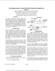
ieee transactions on very large scale integration (vlsi) - Computer ...
ieee transactions on very large scale integration (vlsi) - Computer ...
ieee transactions on very large scale integration (vlsi) - Computer ...

You also want an ePaper? Increase the reach of your titles
YUMPU automatically turns print PDFs into web optimized ePapers that Google loves.
766 IEEE TRANSACTIONS ON VERY LARGE SCALE INTEGRATION (VLSI) SYSTEMS, VOL. 14, NO. 7, JULY 2006<br />
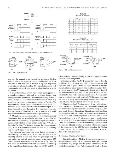
TABLE I<br />
MERGER TRUTH TABLE<br />
TABLE II<br />
MUX ERROR WHEN SEL = X<br />
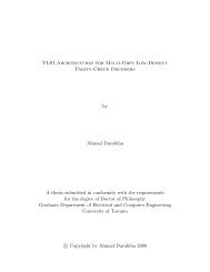
Fig. 4. (a) D-flip-flop. (b) Reset synchr<strong>on</strong>icity. (c) Reset-clock c<strong>on</strong>test.<br />
Fig. 5. MUX implementati<strong>on</strong>s.<br />
reset may be mapped to an element that c<strong>on</strong>tains a flip-flop<br />
with a synchr<strong>on</strong>ous <strong>on</strong>e and vice versa, resulting in a functi<strong>on</strong>al<br />
error, that is, both directi<strong>on</strong>s of the error in Fig. 4(b) may occur.<br />
Clearly, the waveforms from Fig. 4(b) indicate that, when such<br />
a mismapping occurs, it may result in a functi<strong>on</strong>al error in the<br />
test model.<br />
2) Reset-Clock Race Error: Reset-clock race happens due<br />
to module specificati<strong>on</strong> mismatch in the design libraries used<br />
during test model generati<strong>on</strong>. Different libraries may make different<br />
assumpti<strong>on</strong>s about the winner of the c<strong>on</strong>test, which may<br />
result in an err<strong>on</strong>eous implementati<strong>on</strong>, shown in Fig. 4(c). The<br />
right-hand side of that figure depicts the situati<strong>on</strong> where Q is<br />
initially 0 and the clock prevails, whereas in the left part of the<br />
figure the reset line wins the c<strong>on</strong>test. This type of error can arise<br />
from the c<strong>on</strong>test of other lines (e.g., set or hold) as well, and it<br />
may occur in both directi<strong>on</strong>s as in reset synchr<strong>on</strong>icity.<br />
3) Multiplexer Implementati<strong>on</strong> Error: A multiplexer circuit<br />
allows more than <strong>on</strong>e signal to be placed <strong>on</strong> the same line via<br />
time-divisi<strong>on</strong> multiplexing. A typical two-input multiplexer is<br />
implemented with two tri-state buffers and a logic gate, as<br />
shown in Fig. 5(a). The inverter between the two select ports<br />
of the tri-state buffers ensures that line is driven by<br />
<strong>on</strong>ly <strong>on</strong>e input signal at any time.<br />
Two err<strong>on</strong>eous mappings may occur during extracti<strong>on</strong>, as<br />
shown in Fig. 5(b) and (c). In the first <strong>on</strong>e, the inverter is replaced<br />
by a buffer. In that case, when goes high, both tristate<br />
buffers are enabled, causing a merger at the output .<br />
Table I summarizes the truth table for merger in Fig. 5(b). Entries<br />
which are not bold underlined may cause a discrepancy<br />
in the output logic. Furthermore, when <strong>on</strong>e of and is<br />
Fig. 6. MUX-latch implementati<strong>on</strong>s.<br />
driven by logic 1 and the other by 0, a hazardous path is created<br />
between power and ground.<br />
In the other case [see Fig. 5(c)], instead of tri-state buffers, the<br />
multiplexer is err<strong>on</strong>eously mapped to an implementati<strong>on</strong> with<br />
logic and gates. While the logic functi<strong>on</strong> of the two<br />
implementati<strong>on</strong>s agree for most input combinati<strong>on</strong>s, they differ<br />
when is assigned to . As shown by the first row in Table II,<br />
the implementati<strong>on</strong> with and gates drives 0 <strong>on</strong> ,<br />
while the tri-state buffer implementati<strong>on</strong> drives . This difference<br />
in the simulati<strong>on</strong> result may lead ATPG to generate wr<strong>on</strong>g<br />
test vectors. Clearly, any mismapping between these three implementati<strong>on</strong>s<br />
will result in an err<strong>on</strong>eous test model.<br />
4) Multiplexer-Latch Implementati<strong>on</strong> Error: Multiplexerlatch<br />
(MUX-latch) design allows the sampling of signals from<br />
two n<strong>on</strong>overlapping clock domains. As shown in Fig. 6(a), data<br />
from clock domains and are multiplexed into<br />
the D-flip-flop, which is clocked by , the frequency of<br />
which is the sum of the frequencies of and .<br />
The multiplexer in a MUX-latch design can be implemented<br />
with tri-state devices or gates, as illustrated in Fig. 6(b).<br />
These two implementati<strong>on</strong>s have different logic functi<strong>on</strong>s when<br />
and overlap, a situati<strong>on</strong> which may happen<br />
during scan test. In the implementati<strong>on</strong>, the flip-flop<br />
latches . In c<strong>on</strong>trast, can be latched in the tristate<br />
buffer implementati<strong>on</strong>.<br />
B. Clocking Circuitry Error Types<br />
1) Gated Clock Error: Modern devices impose strict power<br />
c<strong>on</strong>sumpti<strong>on</strong> and reliability requirements. Since not all design<br />
comp<strong>on</strong>ents may always need to operate simultaneously, the<br />
gated clock scheme of Fig. 7(a) is comm<strong>on</strong>ly used to disable