ieee transactions on very large scale integration (vlsi) - Computer ...
ieee transactions on very large scale integration (vlsi) - Computer ...
ieee transactions on very large scale integration (vlsi) - Computer ...

Create successful ePaper yourself
Turn your PDF publications into a flip-book with our unique Google optimized e-Paper software.
764 IEEE TRANSACTIONS ON VERY LARGE SCALE INTEGRATION (VLSI) SYSTEMS, VOL. 14, NO. 7, JULY 2006<br />
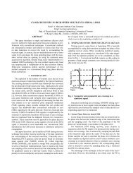
Following test generati<strong>on</strong>, the generated tests are again verified<br />
against the golden model to ensure test correctness, which<br />
is a process known as test (vector) validati<strong>on</strong>. Tests may fail in<br />
this step due to errors introduced in model generati<strong>on</strong> but not<br />
identified during model verificati<strong>on</strong>. When the test model fails,<br />
whether this is during verificati<strong>on</strong> or afterwards during test validati<strong>on</strong>,<br />
manual analysis of the failures is the current industrial<br />
practice, also shown in Fig. 1. This is a daunting task for the test<br />
engineer that may delay test deli<strong>very</strong> to the factories and/or may<br />
reduce their quality.<br />
In this study, we describe a set of extracti<strong>on</strong> errors that<br />
are typical in test model generati<strong>on</strong> for the pipeline comp<strong>on</strong>ent(s)<br />
of high-performance designs that have high frequencies<br />
GHz , c<strong>on</strong>sume little power, and meet strict reliability and<br />
performance c<strong>on</strong>straints [2], [3], [7], [8], [11]. Such errors may<br />
occur because of err<strong>on</strong>eous module mapping during extracti<strong>on</strong><br />
and because of library specificati<strong>on</strong> inaccuracies when complex<br />
hardware such as memory elements, multiple clock domains,<br />
and tri-state devices are integrated together. The manual interference<br />
of the designer/test engineer with the design may also<br />
introduce errors.<br />
We also develop an automated simulati<strong>on</strong>-based debugging<br />
soluti<strong>on</strong> that handles single extracti<strong>on</strong> errors in the pipeline of<br />
test models. The proposed soluti<strong>on</strong> does not assume that there<br />
is any corresp<strong>on</strong>dence of primitives between the transistor-level<br />
schematic and the test model. It also works <strong>on</strong> extracted gatelevel<br />
descripti<strong>on</strong>s with no (and/or partial) state equivalence informati<strong>on</strong><br />
to the transistor-level representati<strong>on</strong>. Lack of state/<br />
primitive equivalence informati<strong>on</strong> between the test model and<br />
the transistor-level schematic increases the problem complexity<br />
and the debugging effort by the designer. It should be noted that<br />
the nature and the effects of extracti<strong>on</strong> errors are radically different<br />
from the well-examined topic of design errors presented<br />
in [1]. For example, unlike the error types described here, the<br />
error model proposed by Abadir et al. [1] does not include primitives<br />
such as flip-flops and tri-state devices, and it does not<br />
apply to functi<strong>on</strong>al errors that arise from err<strong>on</strong>eous timing of the<br />
circuit. Therefore, design-error debugging techniques [18], [19]<br />
may not be applicable/efficient when applied to this problem.<br />
An extensive suite of experiments <strong>on</strong> designs with similar architecture<br />
to that found in industry dem<strong>on</strong>strates the practicality<br />
of the approach. Methods such as the <strong>on</strong>e presented here benefit<br />
the testing of microprocessors, ASICs, and SoCs. They help<br />
in identifying model inaccuracies at early stages of the design<br />
cycle, reducing test deli<strong>very</strong> turnaround time and improving test<br />
model generati<strong>on</strong>.<br />
The remaining paper is structured as follows. Secti<strong>on</strong> II<br />
presents the circuit architecture and gives more details about the<br />
intricacies of the particular problem. Secti<strong>on</strong> III c<strong>on</strong>tains a study<br />
of different types of extracti<strong>on</strong> errors that are typical in a modern<br />
industrial envir<strong>on</strong>ment for high-performance integrated circuits.<br />
Secti<strong>on</strong> IV describes the debugging methodology, and Secti<strong>on</strong> V<br />
presents the experiments. Secti<strong>on</strong> VI c<strong>on</strong>cludes this work.<br />
II. PRELIMINARIES<br />
Extracti<strong>on</strong> builds a logic representati<strong>on</strong>, known as the test<br />
model, from a custom transistor-level block [4]–[6], [10], [13].<br />
This representati<strong>on</strong> is later used for test generati<strong>on</strong>. This work<br />
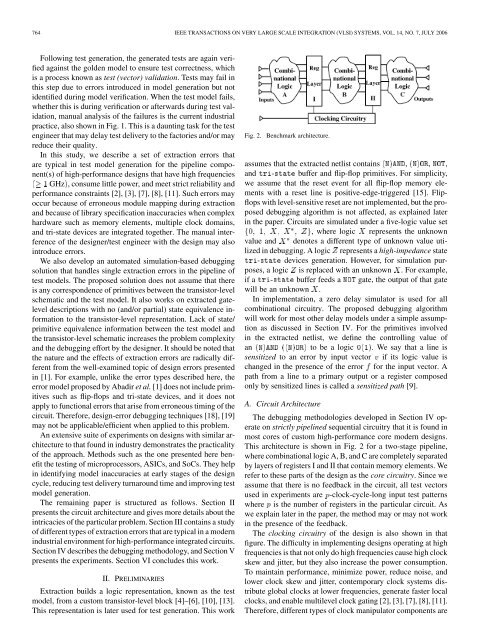
Fig. 2. Benchmark architecture.<br />
assumes that the extracted netlist c<strong>on</strong>tains , , ,<br />
and - buffer and flip-flop primitives. For simplicity,<br />
we assume that the reset event for all flip-flop memory elements<br />
with a reset line is positive-edge-triggered [15]. Flipflops<br />
with level-sensitive reset are not implemented, but the proposed<br />
debugging algorithm is not affected, as explained later<br />
in the paper. Circuits are simulated under a five-logic value set<br />
, where logic represents the unknown<br />
value and denotes a different type of unknown value utilized<br />
in debugging. A logic represents a high-impedance state<br />
- devices generati<strong>on</strong>. However, for simulati<strong>on</strong> purposes,<br />
a logic is replaced with an unknown . For example,<br />
if a - buffer feeds a gate, the output of that gate<br />
will be an unknown .<br />
In implementati<strong>on</strong>, a zero delay simulator is used for all<br />
combinati<strong>on</strong>al circuitry. The proposed debugging algorithm<br />
will work for most other delay models under a simple assumpti<strong>on</strong><br />
as discussed in Secti<strong>on</strong> IV. For the primitives involved<br />
in the extracted netlist, we define the c<strong>on</strong>trolling value of<br />
an to be a logic . We say that a line is<br />
sensitized to an error by input vector if its logic value is<br />
changed in the presence of the error for the input vector. A<br />
path from a line to a primary output or a register composed<br />
<strong>on</strong>ly by sensitized lines is called a sensitized path [9].<br />
A. Circuit Architecture<br />
The debugging methodologies developed in Secti<strong>on</strong> IV operate<br />
<strong>on</strong> strictly pipelined sequential circuitry that it is found in<br />
most cores of custom high-performance core modern designs.<br />
This architecture is shown in Fig. 2 for a two-stage pipeline,<br />
where combinati<strong>on</strong>al logic A, B, and C are completely separated<br />
by layers of registers I and II that c<strong>on</strong>tain memory elements. We<br />
refer to these parts of the design as the core circuitry. Since we<br />
assume that there is no feedback in the circuit, all test vectors<br />
used in experiments are -clock-cycle-l<strong>on</strong>g input test patterns<br />
where is the number of registers in the particular circuit. As<br />
we explain later in the paper, the method may or may not work<br />
in the presence of the feedback.<br />
The clocking circuitry of the design is also shown in that<br />
figure. The difficulty in implementing designs operating at high<br />
frequencies is that not <strong>on</strong>ly do high frequencies cause high clock<br />
skew and jitter, but they also increase the power c<strong>on</strong>sumpti<strong>on</strong>.<br />
To maintain performance, minimize power, reduce noise, and<br />
lower clock skew and jitter, c<strong>on</strong>temporary clock systems distribute<br />
global clocks at lower frequencies, generate faster local<br />
clocks, and enable multilevel clock gating [2], [3], [7], [8], [11].<br />
Therefore, different types of clock manipulator comp<strong>on</strong>ents are