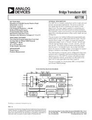
AD548 Precision, Low Power BiFET Op Amp - QRZ.ru
AD548 Precision, Low Power BiFET Op Amp - QRZ.ru
AD548 Precision, Low Power BiFET Op Amp - QRZ.ru

Create successful ePaper yourself
Turn your PDF publications into a flip-book with our unique Google optimized e-Paper software.
<strong>AD548</strong><br />
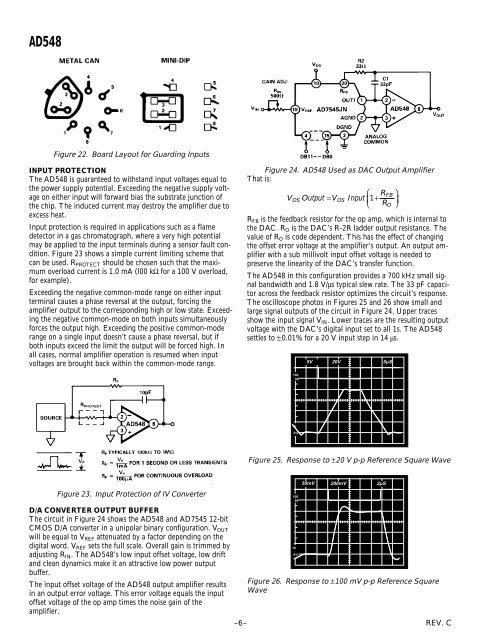
Figure 22. Board Layout for Guarding Inputs<br />
INPUT PROTECTION<br />
The <strong>AD548</strong> is guaranteed to withstand input voltages equal to<br />
the power supply potential. Exceeding the negative supply voltage<br />
on either input will forward bias the substrate junction of<br />
the chip. The induced current may destroy the amplifier due to<br />
excess heat.<br />
Input protection is required in applications such as a flame<br />
detector in a gas chromatograph, where a very high potential<br />
may be applied to the input terminals during a sensor fault condition.<br />
Figure 23 shows a simple current limiting scheme that<br />
can be used. R PROTECT should be chosen such that the maximum<br />
overload current is 1.0 mA (l00 kΩ for a 100 V overload,<br />
for example).<br />
Exceeding the negative common-mode range on either input<br />
terminal causes a phase reversal at the output, forcing the<br />
amplifier output to the corresponding high or low state. Exceeding<br />
the negative common-mode on both inputs simultaneously<br />
forces the output high. Exceeding the positive common-mode<br />
range on a single input doesn’t cause a phase reversal, but if<br />
both inputs exceed the limit the output will be forced high. In<br />
all cases, normal amplifier operation is resumed when input<br />
voltages are brought back within the common-mode range.<br />
Figure 24. <strong>AD548</strong> Used as DAC Output <strong>Amp</strong>lifier<br />
That is:<br />
⎛<br />
V OS Output =V OS Input 1+ R FB ⎞<br />
⎜<br />
⎝ R<br />
⎟<br />
O ⎠<br />
R FB is the feedback resistor for the op amp, which is internal to<br />
the DAC. R O is the DAC’s R-2R ladder output resistance. The<br />
value of R O is code dependent. This has the effect of changing<br />
the offset error voltage at the amplifier’s output. An output amplifier<br />
with a sub millivolt input offset voltage is needed to<br />
preserve the linearity of the DAC’s transfer function.<br />
The <strong>AD548</strong> in this configuration provides a 700 kHz small signal<br />
bandwidth and 1.8 V/µs typical slew rate. The 33 pF capacitor<br />
across the feedback resistor optimizes the circuit’s response.<br />
The oscilloscope photos in Figures 25 and 26 show small and<br />
large signal outputs of the circuit in Figure 24. Upper traces<br />
show the input signal V IN . <strong>Low</strong>er traces are the resulting output<br />
voltage with the DAC’s digital input set to all 1s. The <strong>AD548</strong><br />
settles to ±0.01% for a 20 V input step in 14 µs.<br />
5V 20V<br />
5µS<br />
100<br />
90<br />
10<br />
0%<br />
Figure 25. Response to ±20 V p-p Reference Square Wave<br />
Figure 23. Input Protection of IV Converter<br />
D/A CONVERTER OUTPUT BUFFER<br />
The circuit in Figure 24 shows the <strong>AD548</strong> and AD7545 12-bit<br />
CMOS D/A converter in a unipolar binary configuration. V OUT<br />
will be equal to V REF attenuated by a factor depending on the<br />
digital word. V REF sets the full scale. Overall gain is trimmed by<br />
adjusting R IN . The <strong>AD548</strong>’s low input offset voltage, low drift<br />
and clean dynamics make it an attractive low power output<br />
buffer.<br />
The input offset voltage of the <strong>AD548</strong> output amplifier results<br />
in an output error voltage. This error voltage equals the input<br />
offset voltage of the op amp times the noise gain of the<br />
amplifier.<br />
100<br />
90<br />
10<br />
0%<br />
50mV 200mV<br />
2µS<br />
Figure 26. Response to ±100 mV p-p Reference Square<br />
Wave<br />
–6– REV. C