AD677 16-Bit 100 kSPS Sampling ADC - Analog Devices
AD677 16-Bit 100 kSPS Sampling ADC - Analog Devices
AD677 16-Bit 100 kSPS Sampling ADC - Analog Devices

You also want an ePaper? Increase the reach of your titles
YUMPU automatically turns print PDFs into web optimized ePapers that Google loves.
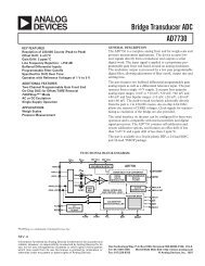
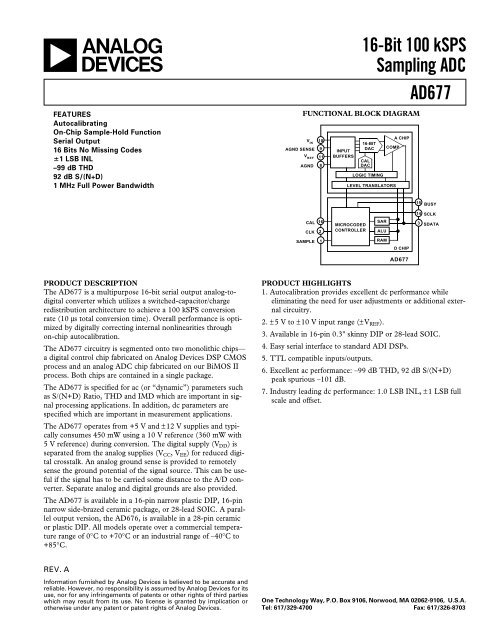
aFEATURESAutocalibratingOn-Chip Sample-Hold FunctionSerial Output<strong>16</strong> <strong>Bit</strong>s No Missing Codes1 LSB INL–99 dB THD92 dB S/(N+D)1 MHz Full Power BandwidthFUNCTIONAL BLOCK DIAGRAMV INAGND SENSEV REFAGND109118INPUTBUFFERS<strong>16</strong>-<strong>Bit</strong> <strong>100</strong> <strong>kSPS</strong><strong>Sampling</strong> <strong>ADC</strong><strong>AD677</strong><strong>16</strong>-BITDACCALDACLOGIC TIMINGCOMPLEVEL TRANSLATORSA CHIP15 BUSY14 SCLKCAL <strong>16</strong>CLK 2MICROCODEDCONTROLLERSARALU3SDATASAMPLE1RAMD CHIP<strong>AD677</strong>PRODUCT DESCRIPTIONThe <strong>AD677</strong> is a multipurpose <strong>16</strong>-bit serial output analog-todigitalconverter which utilizes a switched-capacitor/chargeredistribution architecture to achieve a <strong>100</strong> <strong>kSPS</strong> conversionrate (10 µs total conversion time). Overall performance is optimizedby digitally correcting internal nonlinearities throughon-chip autocalibration.The <strong>AD677</strong> circuitry is segmented onto two monolithic chips—a digital control chip fabricated on <strong>Analog</strong> <strong>Devices</strong> DSP CMOSprocess and an analog <strong>ADC</strong> chip fabricated on our BiMOS IIprocess. Both chips are contained in a single package.The <strong>AD677</strong> is specified for ac (or “dynamic”) parameters suchas S/(N+D) Ratio, THD and IMD which are important in signalprocessing applications. In addition, dc parameters arespecified which are important in measurement applications.The <strong>AD677</strong> operates from +5 V and ±12 V supplies and typicallyconsumes 450 mW using a 10 V reference (360 mW with5 V reference) during conversion. The digital supply (V DD ) isseparated from the analog supplies (V CC , V EE ) for reduced digitalcrosstalk. An analog ground sense is provided to remotelysense the ground potential of the signal source. This can be usefulif the signal has to be carried some distance to the A/D converter.Separate analog and digital grounds are also provided.The <strong>AD677</strong> is available in a <strong>16</strong>-pin narrow plastic DIP, <strong>16</strong>-pinnarrow side-brazed ceramic package, or 28-lead SOIC. A paralleloutput version, the AD676, is available in a 28-pin ceramicor plastic DIP. All models operate over a commercial temperaturerange of 0°C to +70°C or an industrial range of –40°C to+85°C.PRODUCT HIGHLIGHTS1. Autocalibration provides excellent dc performance whileeliminating the need for user adjustments or additional externalcircuitry.2. ±5 V to ±10 V input range (±V REF ).3. Available in <strong>16</strong>-pin 0.3" skinny DIP or 28-lead SOIC.4. Easy serial interface to standard ADI DSPs.5. TTL compatible inputs/outputs.6. Excellent ac performance: –99 dB THD, 92 dB S/(N+D)peak spurious –101 dB.7. Industry leading dc performance: 1.0 LSB INL, ±1 LSB fullscale and offset.REV. AInformation furnished by <strong>Analog</strong> <strong>Devices</strong> is believed to be accurate andreliable. However, no responsibility is assumed by <strong>Analog</strong> <strong>Devices</strong> for itsuse, nor for any infringements of patents or other rights of third partieswhich may result from its use. No license is granted by implication orotherwise under any patent or patent rights of <strong>Analog</strong> <strong>Devices</strong>.One Technology Way, P.O. Box 9106, Norwood, MA 02062-9106, U.S.A.Tel: 617/329-4700 Fax: 617/326-8703
<strong>AD677</strong>–SPECIFICATIONSAC SPECIFICATIONS<strong>AD677</strong>J/A <strong>AD677</strong>K/BParameter Min Typ Max Min Typ Max UnitsTotal Harmonic Distortion (THD) 2@ 83 <strong>kSPS</strong>, T MIN to T MAX –97 –92 –99 –95 dB@ <strong>100</strong> <strong>kSPS</strong>, +25°C –97 –92 –99 –95 dB@ <strong>100</strong> <strong>kSPS</strong>, T MIN to T MAX –93 –95 dBSignal-to-Noise and Distortion Ratio (S/(N+D)) 2, 3@ 83 <strong>kSPS</strong>, T MIN to T MAX 89 91 90 92 dB@ <strong>100</strong> <strong>kSPS</strong>, +25°C 89 91 90 92 dB@ <strong>100</strong> <strong>kSPS</strong>, T MIN to T MAX 89 90 dBPeak Spurious or Peak Harmonic Component –101 –101 dBIntermodulation Distortion (IMD) 42nd Order Products –102 –102 dB3rd Order Products –98 –98 dBFull Power Bandwidth 1 1 MHzNoise <strong>16</strong>0 <strong>16</strong>0 µV rmsDIGITAL SPECIFICATIONSParameter Test Conditions Min Typ Max UnitsLOGIC INPUTSV IH High Level Input Voltage 2.0 V DD + 0.3 VV IL Low Level Input Voltage –0.3 0.8 VI IH High Level Input Current V IH = V DD –10 +10 µAI IL Low Level Input Current V IL = 0 V –10 +10 µAC IN Input Capacitance 10 pFLOGIC OUTPUTSV OH High Level Output Voltage I OH = 0.1 mA V DD – 1 V VI OH = 0.5 mA 2.4 VV OL Low Level Output Voltage I OL = 1.6 mA 0.4 VNOTES1 V REF = 10.0 V, Conversion Rate = <strong>100</strong> <strong>kSPS</strong>, f lN = 1.0 kHz, V IN = –0.05 dB, Bandwidth = 50 kHz unless otherwise indicated. All measurements referred to a 0 dB(20 V p-p) input signal. Values are post-calibration.2 For other input amplitudes, refer to Figure 12.3 For dynamic performance with different reference values see Figure 11.4 fa = <strong>100</strong>8 Hz, fb = 1055 Hz. See Definition of Specifications section and Figure <strong>16</strong>.Specifications subject to change without notice.(T MIN to T MAX, V CC = +12 V 5%, V EE = –12 V 5%, V DD = +5 V 10%) 1(for all grades T MIN to T MAX , V CC = +12 V 5%, V EE = –12 V 5%, V DD = +5 V 10%)–2–REV. A
DC SPECIFICATIONS(T MIN to T MAX , V CC = +12 V 5%, V EE = –12 V 5%, V DD = +5 V 1O%) 1<strong>AD677</strong><strong>AD677</strong>J/A<strong>AD677</strong>K/BParameter Min Typ Max Min Typ Max UnitsTEMPERATURE RANGEJ, K Grades 0 +70 0 +70 °CA, B Grades –40 +85 –40 +85 °CACCURACYResolution <strong>16</strong> <strong>16</strong> <strong>Bit</strong>sIntegral Nonlinearity (INL)@ 83 <strong>kSPS</strong>, T MIN to T MAX ±1 ±1 ±1.5 LSB@ <strong>100</strong> <strong>kSPS</strong>, +25°C ±1 +1 ±1.5 LSB@ <strong>100</strong> <strong>kSPS</strong>, T MIN to T MAX ±2 ±2 LSBDifferential Nonlinearity (DNL)–No Missing Codes <strong>16</strong> <strong>16</strong> <strong>Bit</strong>sBipolar Zero Error 2 ±2 ±4 ±1 ±3 LSBPositive, Negative FS Errors 2@ 83 <strong>kSPS</strong> ±2 ±4 ±1 ±3 LSB@ <strong>100</strong> <strong>kSPS</strong>, +25°C ±2 ±4 ±1 ±3 LSB@ <strong>100</strong> <strong>kSPS</strong> ±4 ±4 LSBTEMPERATURE DRIFT 3Bipolar Zero ±0.5 ±0.5 LSBPostive Full Scale ±0.5 ±0.5 LSBNegative Full Scale ±0.5 ±0.5 LSBVOLTAGE REFERENCE INPUT RANGE 4 (V REF ) 5 10 5 10 VANALOG INPUT 5Input Range (V IN ) ±V REF ±V REF VInput Impedance * *Input Settling Time 2 2 µsInput Capacitance During Sample 50* 50* pFAperture Delay 6 6 nsAperture Jitter <strong>100</strong> <strong>100</strong> psPOWER SUPPLIESPower Supply Rejection 6V CC = +12 V ± 5% ±0.5 ±0.5 LSBV EE = –12 V ± 5% ±0.5 ±0.5 LSBV DD = +5 V ± 10% ±0.5 ±0.5 LSBOperating CurrentV REF = +5 VI CC 14.5 18 14.5 18 mAI EE 14.5 18 14.5 18 –mAI DD 3 5 3 5 mAPower Consumption 360 480 360 480 mWV REF = +10 VI CC 18 24 18 24 mAI EE 18 24 18 24 –mAI DD 3 5 3 5 mAPower Consumption 450 630 450 630 mWNOTES1 V REF = 10.0 V, Conversion Rate = <strong>100</strong> <strong>kSPS</strong> unless otherwise noted. Values are post-calibration.2 Values shown apply to any temperature from T MIN to T MAX after calibration at that temperature at nominal supplies.3 Values shown are based upon calibration at +25°C with no additional calibration at temperature. Values shown are the typical variation from the value at +25 °C.4 See “APPLICATIONS” section for recommended voltage reference circuit, and Figure 11 for dynamic performance with other reference voltage values.5 See “APPLICATIONS” section for recommended input buffer circuit.6 Typical deviation of bipolar zero, –full scale or +full scale from min to max rating.*For explanation of input characteristics, see “ANALOG INPUT” section.Specifications subject to change without notice.REV. A –3–
<strong>AD677</strong>TIMING SPECIFICATIONS (T MIN to T MAX , V CC = +12 V 5%, V EE = –12 V 5%, V DD = +5 V 10%) 1Parameter Symbol Min Typ Max UnitsConversion Period 2, 3 t C 10 <strong>100</strong>0 µsCLK Period 4 t CLK 480 nsCalibration Time t CT 85532 t CLK<strong>Sampling</strong> Time t S 2 µsLast CLK to SAMPLE Delay 5 t LCS 2.1 µsSAMPLE Low t SL <strong>100</strong> nsSAMPLE to Busy Delay t SS 30 75 ns1st CLK Delay t FCD 50 nsCLK Low 6 t CL 50 nsCLK High 6 t CH 50 nsCLK to BUSY Delay t CB 180 300 nsCLK to SDATA Valid t CD 50 <strong>100</strong> 175 nsCLK to SCLK High t CSH <strong>100</strong> 180 300 nsSCLK Low t SCL 50 80 nsSDATA to SCLK High t DSH 50 80 nsCAL High Time t CALH 50 nsCAL to BUSY Delay t CALB 15 50 nsNOTES1 See the “CONVERSION CONTROL” and “AUTOCALIBRATION” sections for detailed explanations of the above timing.2 Depends upon external clock frequency; includes acquisition time and conversion time. The maximum conversion period is specified to account for the droop of theinternal sample/hold function. Operation at slower rates may degrade performance.3 t C = t FCD + <strong>16</strong> × t CLK + t LCS .4 580 ns is recommended for optimal accuracy over temperature (not necessary during calibration cycle).5 If SAMPLE goes high before the 17th CLK pulse, the device will start sampling approximately <strong>100</strong> ns after the rising edge of the 17th CLK pulse.6 t CH + t CL = t CLK and must be greater than 480 ns.CAL(INPUT)t CALHt CTBUSY(OUTPUT)t CALBCLK*(INPUT)t FCDt CB1 2 385530 85531 85532t CHt CLt CLK*SHADED PORTIONS OF INPUT SIGNALS ARE OPTIONAL. FOR BEST PERFORMANCE, WERECOMMEND THAT THESE SIGNALS BE HELD LOW EXCEPT WHEN EXPLICITY SHOWN HIGH.Figure 1. Calibration Timingt CLt CSHt SSAMPLE*t SLt C(INPUT)t SBBUSY(OUTPUT)t FCDt CBt CHCLK*(INPUT) 1 2 3 15 <strong>16</strong> 17t CLKt LCSt SSCLK(OUTPUT)t CDt SCLt DSHSDATA(OUTPUT)OLD BIT <strong>16</strong>MSBBIT BIT BIT BIT2 13 14 15BIT<strong>16</strong>*SHADED PORTIONS OF INPUT SIGNALS ARE OPTIONAL. FOR BEST PERFORMANCE, WERECOMMEND THAT THESE SIGNALS BE HELD LOW EXCEPT WHEN EXPLICITY SHOWN HIGH.Figure 2. General Conversion Timing–4–REV. A
<strong>AD677</strong>ORDERING GUIDETemperaturePackageModel Range S/(N+D) Max INL Package Description Option*<strong>AD677</strong>JN 0°C to +70°C 89 dB Typ Only Plastic <strong>16</strong>-Pin DIP N-<strong>16</strong><strong>AD677</strong>KN 0°C to +70°C 90 dB ±1.5 LSB Plastic <strong>16</strong>-Pin DIP N-<strong>16</strong><strong>AD677</strong>JD 0°C to +70°C 89 dB Typ Only Ceramic <strong>16</strong>-Pin DIP D-<strong>16</strong><strong>AD677</strong>KD 0°C to +70°C 90 dB ±1.5 LSB Ceramic <strong>16</strong>-Pin DIP D-<strong>16</strong><strong>AD677</strong>JR 0°C to +70°C 89 dB Typ Only Plastic 28-Lead SOIC R-28<strong>AD677</strong>KR 0°C to +70°C 90 dB ±1.5 LSB Plastic 28-Lead SOIC R-28<strong>AD677</strong>AD –40°C to +85°C 89 dB Typ Only Ceramic <strong>16</strong>-Pin DIP D-<strong>16</strong><strong>AD677</strong>BD –40°C to +85°C 90 dB ±1.5 LSB Ceramic <strong>16</strong>-Pin DIP D-<strong>16</strong>*D = Ceramic DIP; N = Plastic DIP; R = Small Outline IC (SOIC).ABSOLUTE MAXIMUM RATINGS*V CC to V EE . . . . . . . . . . . . . . . . . . . . . . . . . . . . –0.3 V to +26.4 VV DD to DGND . . . . . . . . . . . . . . . . . . . . . . . . . . . . –0.3 V to +7 VVcc to AGND . . . . . . . . . . . . . . . . . . . . . . . . . . . –0.3 V to +18 VVEE to AGND . . . . . . . . . . . . . . . . . . . . . . . . . . –18 V to +0.3 VAGND to DGND . . . . . . . . . . . . . . . . . . . . . . . . . . . . . . . +0.3 VDigiul Inputs to DGND . . . . . . . . . . . . . . . . . . . . . . 0 to +5.5 V<strong>Analog</strong> Inputs, V REF to AGND. . . . . . . . . . . . . . . . . . . . . . . . . . . . (V CC +0.3 V) to (V EE –0.3 V)Soldering . . . . . . . . . . . . . . . . . . . . . . . . . . . . . . . +300°C, 10 secStorage Temperature . . . . . . . . . . . . . . . . . . . . .–65°C to +150°C*Stresses greater than those listed under “Absolute Maximum Ratings” may causepermanent damage to the device. This is a stress rating only and functionaloperation of the device at these or any other conditions above those indicated in theoperational section of this specification is not implied. Exposure to absolutemaximum rating conditions for extended periods may affect device reliability.CAUTIONESD (electrostatic discharge) sensitive device. Electrostatic charges as high as 4000 V readilyaccumulate on the human body and test equipment and can discharge without detection.Although the <strong>AD677</strong> features proprietary ESD protection circuitry, permanent damage mayoccur on devices subjected to high energy electrostatic discharges. Therefore, proper ESDprecautions are recommended to avoid performance degradation or loss of functionality.WARNING!ESD SENSITIVE DEVICEREV. A –5–
<strong>AD677</strong>PIN DESCRIPTIONDIP Pin SOIC Pin Type Name Description1 1 SAMPLE DI V IN Acquisition Control Pin. Active HIGH. During conversion, SAMPLEcontrols the suite of the internal sample-hold amplifier and the falling edgeinitiates conversion. During calibration, SAMPLE should be held LOW. IfHIGH during calibration, diagnostic information will appear on SDATA.2 2 CLK DI Master Clock Input. The <strong>AD677</strong> requires 17 clock pulses to execute aconversion. CLK is also used to derive SCLK.3 3 SDATA DO Serial Output Data Controlled by SCLK.4 6, 7 DGND P Digital Ground.5 8 V CC P +12 V <strong>Analog</strong> Supply Voltage.8 12 AGND P <strong>Analog</strong> Ground..9 15 AGND SENSE AI <strong>Analog</strong> Ground Sense.10 <strong>16</strong> V IN AI <strong>Analog</strong> Input Voltage.11 17 V REF AI External Voltage Reference Input.12 21 V EE P –12 V <strong>Analog</strong> Supply Voltage.13 22, 23 V DD P +5 V Logic Supply Voltage.14 26 SCLK DO Clock Output for Data Read, derived from CLK.15 27 BUSY DO Status Line for Converter. Active HIGH, indicating a conversion orcalibration in progress.<strong>16</strong> 28 CAL DI Calibration Control Pin.6, 7 4, 5, 9, 10, 11, NC _ No Connection. No connections should be made to these pins.13, 14, 18, 19,20, 24, 25Type:AI = <strong>Analog</strong> InputDI = Digital InputDO = Digital OutputP = PowerSAMPLE1<strong>16</strong>CALSAMPLE128CALCLK215BUSYCLK227BUSYSDATADGNDV CCNCNCAGND345678<strong>AD677</strong>TOP VIEW(Not to Scale)NC = NO CONNECTDIP Pinout14131211109SCLKV DDV EEV REFV INAGNDSENSESDATANCNCDGND1DGND2V CCNCNCNC34578910112625246 23<strong>AD677</strong>TOP VIEW(Not to Scale)2221201918SCLKNCNCV DD1V DD2V EENCNCNCAGND1217V REFNC13<strong>16</strong>V INNC1415AGNDSENSENC = NO CONNECTSOIC Pinout–6–REV. A
Definition of Specifications–<strong>AD677</strong>NYQUIST FREQUENCYAn implication of the Nyquist sampling theorem, the “Nyquistfrequency’’ of a converter is that input frequency which is onehalf the sampling frequency of the converter.TOTAL HARMONIC DISTORTIONTotal harmonic distortion (THD) is the ratio of the rms sum ofthe harmonic components to the rms value of a full-scale inputsignal and is expressed in percent (%) or decibels (dB). For inputsignals or harmonics that are above the Nyquist frequency,the aliased components are used.SIGNAL-TO-NOISE PLUS DISTORTION RATIOSignal-to-noise plus distortion is defined to be the ratio of therms value of the measured input signal to the rms sum of allother spectral components below the Nyquist frequency, includingharmonics but excluding dc.+/– FULL-SCALE ERRORThe last + transition (from 011 . . . 10 to 011 . . . 11) shouldoccur for an analog voltage 1.5 LSB below the nominal fullscale (4.99977 volts for a ±5 V range). The full-scale error isthe deviation of the actual level of the last transition from theideal level.BIPOLAR ZERO ERRORBipolar zero error is the difference between the ideal midscaleinput voltage (0 V) and the actual voltage producing the midscaleoutput code.DIFFERENTIAL NONLINEARITY (DNL)In an ideal <strong>ADC</strong>, code transitions are one LSB apart. Differentialnonlinearity is the maximum deviation from this ideal value.It is often specified in terms of resolution for which no missingcodes are guaranteed.INTEGRAL NONLINEARITY (INL)The ideal transfer function for an <strong>ADC</strong> is a straight line bisectingthe center of each code drawn between “zero” and “fullscale.” The point used as “zero” occurs 1/2 LSB before themost negative code transition. “Full scale” is defined as a level1.5 LSB beyond the most positive code transition. Integral nonlinearityis the worst-case deviation of a code center averagefrom the straight line.BANDWIDTHThe full-power bandwidth is that input frequency at which theamplitude of the reconstructed fundamental is reduced by 3 dBfor a full-scale input.INTERMODULATION DISTORTION (IMD)With inputs consisting of sine waves at two frequencies, fa andfb, any device with nonlinearities will create distortion products,of order (m+n), at sum and difference frequencies of mfa ± nfb,where m, n = 0, 1, 2, 3 . . . . Intermodulation terms are thosefor which m or n is not equal to zero. For example, the secondorder terms are (fa + fb) and (fa – fb), and the third order termsare (2 fa + fb), (2 fa – fb), (fa + 2 fb) and (fa – 2 fb). The IMDproducts are expressed as the decibel ratio of the rms sum of themeasured input signals to the rms sum of the distortion terms.The two signals applied to the converter are of equal amplitude,and the peak value of their sum is –0.5 dB from full scale. TheIMD products are normalized to a 0 dB input signal.APERTURE DELAYAperture delay is the time required after SAMPLE pin is takenLOW for the internal sample-hold of the <strong>AD677</strong> to open, thusholding the value of V IN .APERTURE JITTERAperture jitter is the variation in the aperture delay from sampleto sample.POWER SUPPLY REJECTIONDC variations in the power supply voltage will affect the overalltransfer function of the <strong>ADC</strong>, resulting in zero error and fullscaleerror changes. Power supply rejection is the maximumchange in either the bipolar zero error or full-scale error value.Additionally, there is another power supply variation to consider.AC ripple on the power supplies can couple noise into the<strong>ADC</strong>, resulting in degradation of dynamic performance. This isdisplayed in Figure 15.INPUT SETTLING TIMESettling time is a function of the SHA’s ability to track fastslewing signals. This is specified as the maximum time requiredin track mode after a full-scale step input to guarantee ratedconversion accuracy.NOISE/DC CODE UNCERTAINTYIdeally, a fixed dc input should result in the same output codefor repetitive conversions. However, as a consequence of unavoidablecircuit noise within the wideband circuits in the <strong>ADC</strong>,there is a range of output codes which may occur for a given inputvoltage. If you apply a dc signal to the <strong>ADC</strong> and record alarge number of conversions, the result will be a distribution ofcodes. If you fit a Gaussian probability distribution to the histogram,the standard deviation is approximately equivalent to therms input noise of the <strong>ADC</strong>.REV. A –7–
<strong>AD677</strong>FUNCTIONAL DESCRIPTIONThe <strong>AD677</strong> is a multipurpose <strong>16</strong>-bit analog-to-digital converterand includes circuitry which performs an input sample/holdfunction, ground sense, and autocalibration. These functionsare segmented onto two monolithic chips—an analog signal processorand a digital controller. Both chips are contained withinthe <strong>AD677</strong> package.The <strong>AD677</strong> employs a successive-approximation technique todetermine the value of the analog input voltage. However, insteadof the traditional laser-trimmed resistor-ladder approach,this device uses a capacitor-array, charge redistribution technique.Binary-weighted capacitors subdivide the input sample toperform the actual analog-to-digital conversion. The capacitorarray eliminates variation in the linearity of the device due totemperature-induced mismatches of resistor values. Since acapacitor array is used to perform the data conversions, thesample/hold function is included without the need for additionalexternal circuitry.Initial errors in capacitor matching are eliminated by anautocalibration circuit within the <strong>AD677</strong>. This circuit employsan on-chip microcontroller and a calibration DAC to measureand compensate capacitor mismatch errors. As each error isdetermined, its value is stored in on-chip memory (RAM).Subsequent conversions use these RAM values to improve conversionaccuracy. The autocalibration routine may be invokedat any time. Autocalibration insures high performance whileeliminating the need for any user adjustments and is describedin detail below.The microcontroller controls all of the various functions withinthe <strong>AD677</strong>. These include the actual successive approximationalgorithm, the autocalibration routine, the sample/hold operation,and the internal output data latch.AUTO CALIBRATIONThe <strong>AD677</strong> achieves rated performance without the need foruser trims or adjustments. This is accomplished through the useof on-chip autocalibration.In the autocalibration sequence, sample/hold offset is nulled byinternally connecting the input circuit to the ground sense circuit.The resulting offset voltage is measured and stored inRAM for later use. Next, the capacitor representing the mostsignificant bit (MSB) is charged to the reference voltage. Thischarge is then transferred to a capacitor of equal size (composedof the sum of the remaining lower weight bits). The voltage thatresults represents the amount of capacitor mismatch. A calibrationdigital-to-analog converter (DAC) adds an appropriatevalue of error correction voltage to cancel this mismatch. Thiscorrection factor is also stored in RAM. This process is repeatedfor each of the eight remaining capacitors representing the topnine bits. The accumulated values in RAM are then used duringsubsequent conversions to adjust conversion results accordingly.As shown in Figure 1, when CAL is taken HIGH the <strong>AD677</strong>internal circuitry is reset, the BUSY pin is driven HIGH, andthe <strong>ADC</strong> prepares for calibration. This is an asynchronous hardwarereset and will interrupt any conversion or calibration currentlyin progress. Actual calibration begins when CAL is takenLOW and completes in 85,532 clock cycles, indicated by BUSYgoing LOW. During calibration, it is preferable for SAMPLE tobe held LOW. If SAMPLE is HIGH, diagnostic data will appearon SDATA. This data is of no value to the user.In most applications, it is sufficient to calibrate the <strong>AD677</strong> onlyupon power-up, in which case care should be taken that thepower supplies and voltage reference have stabilized first. Ifcalibration is not performed, the <strong>AD677</strong> may come up in an unknownstate, or performance could degrade to as low as 10 bits.CONVERSION CONTROLThe <strong>AD677</strong> is controlled by two signals: SAMPLE and CLK,as shown in Figure 2. It is assumed that the part has been calibratedand the digital I/O pins have the levels shown at the startof the timing diagram.A conversion consists of an input acquisition followed by 17clock pulses which execute the <strong>16</strong>-bit internal successive approximationroutine. The analog input is acquired by taking theSAMPLE line HIGH for a minimum sampling time of t S . Theactual sample taken is the voltage present on V IN one aperturedelay after the SAMPLE line is brought LOW, assuming theprevious conversion has completed (signified by BUSY goingLOW). Care should be taken to ensure that this negative edge iswell defined and jitter free in ac applications to reduce the uncertainty(noise) in signal acquisition. With SAMPLE goingLOW, the <strong>AD677</strong> commits itself to the conversion—the inputat V IN is disconnected from the internal capacitor array, BUSYgoes HIGH, and the SAMPLE input will be ignored until theconversion is completed (when BUSY goes LOW). SAMPLEmust be held LOW for a minimum period of time t SL . A periodof time t FCD after bringing SAMPLE LOW, the 17 CLK cyclesare applied; CLK pulses that start before this period of time areignored. BUSY goes HIGH t SB after SAMPLE goes LOW, signifyingthat a conversion is in process, and remains HIGH untilthe conversion is completed. As indicated in Figure 2, the twoscomplement output data is presented MSB first. This data maybe captured with the rising edge of SCLK or the falling edge ofCLK, beginning with pulse #2. The <strong>AD677</strong> will ignore CLKafter BUSY has gone LOW and SDATA or SCLK will notchange until a new sample is acquired.CONTINUOUS CONVERSIONFor maximum throughput rate, the <strong>AD677</strong> can be operated in acontinuous convert mode. This is accomplished by utilizing thefact that SAMPLE will no longer be ignored after BUSY goesLOW, so an acquisition may be initiated even during the HIGHtime of the 17th CLK pulse for maximum throughput ratewhile enabling full settling of the sample/hold circuitry. IfSAMPLE is already HIGH during the rising edge of the 17thCLK, then an acquisition is immediately initiated approximately<strong>100</strong> ns after the rising edge of the 17th clock pulse.Care must be taken to adhere to the minimum/maximum timingrequirements in order to preserve conversion accuracy.GENERAL CONVERSION GUIDELINESDuring signal acquisition and conversion, care should be takenwith the logic inputs to avoid digital feedthrough noise. It ispossible to run CLK continuously, even during the sampleperiod. However, CLK edges during the sampling period, andespecially when SAMPLE goes LOW, may inject noise into thesampling process. The <strong>AD677</strong> is tested with no CLK cyclesduring the sampling period. The BUSY signal can be used toprevent the clock from running during acquisition, as illustrated–8–REV. A
<strong>AD677</strong>in Figure 3. In this circuit BUSY is used to reset the circuitrywhich divides the system clock down to provide the <strong>AD677</strong>CLK. This serves to interrupt the clock until after the input signalhas been acquired, which has occurred when BUSY goesHIGH. When the conversion is completed and BUSY goesLOW, the circuit in Figure 3 truncates the 17th CLK pulsewidth which is tolerable because only its rising edge is critical.12.288MHzSYSTEMCLOCK11 3Q49<strong>16</strong>21DCLK2Q 73D 12CLR 11Q2D74HC1751CLK13 2CLK1QD12 2CLR1CLR2QC2QD74HC393Figure 3.2598BUSYCLK<strong>AD677</strong>SAMPLEFigure 3 also illustrates the use of a counter (74HC393) to derivethe <strong>AD677</strong> SAMPLE command from the system clockwhen a continuous convert mode is desirable. Pin 9 (2QC) providesa 96 kHz sample rate for the <strong>AD677</strong> when used with a12.288 MHz system clock. Alternately, Pin 8 (2QD) could beused for a 48 kHz rate.If a continuous clock is used, then the user must avoid CLKedges at the instant of disconnecting V IN which occurs at thefalling edge of SAMPLE (see t FCD specification). The duty cycleof CLK may vary, but both the HIGH (t CH ) and LOW (t CL )phases must conform to those shown in the timing specifications.The internal comparator makes its decisions on the risingedge of CLK. To avoid a negative edge transition disturbing thecomparator’s settling, t CL should be at least half the value oft CLK . It is not recommended that the SAMPLE pin change statetoward the end of a CLK cycle, in order to avoid transitions disturbingthe internal comparator’s settling.During a conversion, internal dc error terms such as comparatorvoltage offset are sampled, stored on internal capacitors andused to correct for their corresponding errors when needed. Becausethese voltages are stored on capacitors, they are subject toleakage decay and so require refreshing. For this reason there isa maximum conversion time t C (<strong>100</strong>0 µs). From the timeSAMPLE goes HIGH to the completion of the 17th CLK pulse,no more than <strong>100</strong>0 µs should elapse for specified performance.However, there is no restriction to the maximum time betweenindividual conversions.Output coding for the <strong>AD677</strong> is twos complement as shown inTable I. The <strong>AD677</strong> is designed to limit output coding in theevent of out-of-range input.Table I. Serial Output Coding Format (Twos Complement)V INOutput Code
<strong>AD677</strong>Additionally, it is beneficial to have large capacitors (>47 µF)located at the point where the power connects to the PCB with10 µF capacitors located in the vicinity of the <strong>ADC</strong> to furtherreduce low frequency ripple. In systems that will be subjected toparticularly harsh environmental noise, additional decouplingmay be necessary. RC-filtering on each power supply combinedwith dedicated voltage regulation can substantially decreasepower supply ripple effects (this is further detailed in Figure 7).BOARD LAYOUTDesigning with high resolution data converters requires carefulattention to board layout. Trace impedance is a significant issue.A 1.22 mA current through a 0.5 Ω trace will develop a voltagedrop of 0.6 mV, which is 4 LSBs at the <strong>16</strong>-bit level for a 10 Vfull-scale span. In addition to ground drops, inductive and capacitivecoupling need to be considered, especially when high accuracyanalog signals share the same board with digital signals.<strong>Analog</strong> and digital signals should not share a common returnpath. Each signal should have an appropriate analog or digitalreturn routed close to it. Using this approach, signal loops enclosea small area, minimizing the inductive coupling of noise.Wide PC tracks, large gauge wire, and ground planes are highlyrecommended to provide low impedance signal paths. Separateanalog and digital ground planes are also desirable, with a singleinterconnection point at the <strong>AD677</strong> to minimize interferencebetween analog and digital circuitry. <strong>Analog</strong> signals should berouted as far as possible from digital signals and should crossthem, if at all, only at right angles. A solid analog ground planearound the <strong>AD677</strong> will isolate it from large switching groundcurrents. For these reasons, the use of wire wrap circuit constructionwill not provide adequate performance; careful printedcircuit board construction is preferred.GROUNDINGThe <strong>AD677</strong> has three grounding pins, designated ANALOGGROUND (AGND), DIGITAL GROUND (DGND) andANALOG GROUND SENSE (AGND SENSE). The analogground pin is the “high quality” ground reference point for thedevice, and should be connected to the analog common point inthe system.AGND SENSE is intended to be connected to the input signalground reference point. This allows for slight differences in levelbetween the analog ground point in the system and the inputsignal ground point. However no more than <strong>100</strong> mV is recommendedbetween the AGND and the AGND SENSE pins forspecified performance.Using AGND SENSE to remotely sense the ground potential ofthe signal source can be useful if the signal has to be carriedsome distance to the A/D converter. Since all IC ground currentshave to return to the power supply and no ground leadsare free from resistance and inductance, there are always somevoltage differences from one ground point in a system to another.Over distance this voltage difference can easily amount to severalLSBs (in a 10 V input span, <strong>16</strong>-bit system each LSB isabout 0.15 mV). This would directly corrupt the A/D input signalif the A/D measures its input with respect to power ground(AGND) as shown in Figure 5a. To solve this problem the<strong>AD677</strong> offers an AGND SENSE pin. Figure 5b shows how theAGND SENSE can be used to eliminate the problem in Figure5a. Figure 5b also shows how the signal wires should beSOURCEV S∆VGROUND LEAD I GROUND > 0<strong>AD677</strong>V INAGNDTO POWERSUPPLY GNDFigure 5a. Input to the A/D is Corrupted by IR Drop inGround Leads: V IN = V S + ∆V.SOURCEV SSHIELDED CABLEGROUND LEAD I GROUND > 0<strong>AD677</strong>V INAGNDSENSEAGNDTO POWERSUPPLY GNDFigure 5b. AGND SENSE Eliminates the Problem inFigure 5a.shielded in a noisy environment to avoid capacitive coupling. Ifinductive (magnetic) coupling is expected to be dominant suchas where motors are present, twisted-pair wires should be usedinstead.The digital ground pin is the reference point for all of the digitalsignals that operate the <strong>AD677</strong>. This pin should be connectedto the digital common point in the system. As Figure 4 illustrated,the analog and digital grounds should be connectedtogether at one point in the system, preferably at the <strong>AD677</strong>.VOLTAGE REFERENCEThe <strong>AD677</strong> requires the use of an external voltage reference.The input voltage range is determined by the value of the referencevoltage; in general, a reference voltage of n volts allows aninput range of ±n volts. The <strong>AD677</strong> is specified for a voltagereference between +5 V and +10 V. A 10 V reference will typicallyrequire support circuitry operated from ±15 V supplies; a5.0 V reference may be used with ±12 V supplies. Signal-tonoiseperformance is increased proportionately with input signalrange (see Figure 12). In the presence of a fixed amount of systemnoise, increasing the LSB size (which results from increasingthe reference voltage) will increase the effective S/(N+D)performance. Figure 11 illustrates S/(N+D) as a function of referencevoltage. In contrast, dc accuracy will be optimal at lowerreference voltage values (such as 5 V) due to capacitor nonlinearityat higher voltage values.During a conversion, the switched capacitor array of the <strong>AD677</strong>presents a dynamically changing current load at the voltage referenceas the successive-approximation algorithm cycles throughvarious choices of capacitor weighting. (See the following section“<strong>Analog</strong> Input” for a detailed discussion of the V REF inputcharacteristics.) The output impedance of the reference circuitrymust be low so that the output voltage will remain sufficientlyconstant as the current drive changes. In some applications, thismay require that the output of the voltage reference be bufferedby an amplifier with low impedance at relatively high frequencies.In choosing a voltage reference, consideration should be–10–REV. A
<strong>AD677</strong>made for selecting one with low noise. A capacitor connectedbetween REF IN and AGND will reduce the demands on thereference by decreasing the magnitude of high frequency componentsrequired to be sourced by the reference.Figures 6 and 7 represent typical design approaches.C N1.0µF+12V28 6V REFAD586V IN10µF 0.1µF4Figure 6.<strong>AD677</strong>AGNDFigure 6 shows a voltage reference circuit featuring the 5 V outputAD586. The AD586 is a low cost reference which utilizes aburied Zener architecture to provide low noise and drift. Overthe 0°C to +70°C range, the AD586M grade exhibits less than1.0 mV output change from its initial value at +25°C. A noisereduction capacitor, C N , reduces the broadband noise of theAD586 output, thereby optimizing the overall performance ofthe <strong>AD677</strong>. It is recommended that a 10 µF to 47 µF high qualitytantalum capacitor and a 0.1 µF capacitor be tied betweenthe V REF input of the <strong>AD677</strong> and ground to minimize the impedanceon the reference.Using the <strong>AD677</strong> with ±10 V input range (V REF = 10 V) typicallyrequires ±15 V supplies to drive op amps and the voltagereference. If ±12 V is not available in the system, regulatorssuch as 78L12 and 79L12 can be used to provide power for the<strong>AD677</strong>. This is also the recommended approach (for any inputrange) when the <strong>ADC</strong> system is subjected to harsh environmentssuch as where the power supplies are noisy and wherevoltage spikes are present. Figure 7 shows an example of such asystem based upon the 10 V AD587 reference, which provides a300 µV LSB. Circuitry for additional protection against powersupply disturbances has been shown. A <strong>100</strong> µF capacitor at each10Ω10µF0.1µFAD5872 V IN V O6GND4NR81µFregulator prevents very large voltage spikes from entering theregulators. Any power line noise which the regulators cannoteliminate will be further filtered by an RC filter (10 Ω/10 µF)having a –3 dB point at 1.6 kHz. For best results the regulatorsshould be within a few centimeters of the <strong>AD677</strong>.ANALOG INPUTAs previously discussed, the analog input voltage range for the<strong>AD677</strong> is ±V REF . For purposes of ground drop and commonmode rejection, the V IN and V REF inputs each have their ownground. V REF is referred to the local analog system ground(AGND), and V IN is referred to the analog ground sense pin(AGND SENSE) which allows a remote ground sense for theinput signal.The <strong>AD677</strong> analog inputs (V IN , V REF and AGND SENSE) exhibitdynamic characteristics. When a conversion cycle begins,each analog input is connected to an internal, discharged 50 pFcapacitor which then charges to the voltage present at the correspondingpin. The capacitor is disconnected when SAMPLE istaken LOW, and the stored charge is used in the subsequentconversion. In order to limit the demands placed on the externalsource by this high initial charging current, an internal bufferamplifier is employed between the input and this capacitance fora few hundred nanoseconds. During this time the input pin exhibitstypically 20 kΩ input resistance, 10 pF input capacitanceand ±40 µA bias current. Next, the input is switched directly tothe now precharged capacitor and allowed to fully settle. Duringthis time the input sees only a 50 pF capacitor. Once the sampleis taken, the input is internally floated so that the external inputsource sees a very high input resistance and a parasitic inputcapacitance of typically only 2 pF. As a result, the only dominantinput characteristic which must be considered is the highcurrent steps which occur when the internal buffers are switchedin and out.In most cases, these characteristics require the use of an externalop amp to drive the input of the <strong>AD677</strong>. Care should be takenwith op amp selection; even with modest loading conditions,most available op amps do not meet the low distortion requirementsnecessary to match the performance capabilities of the<strong>AD677</strong>. Figure 8 represents a circuit, based upon the AD845,which will provide excellent overall performance.For applications optimized more for low distortion and lownoise, the AD845 of Figure 8 may be replaced by the AD743.1k Ω+15V<strong>100</strong>µF+5V–15V<strong>100</strong>µF78L12<strong>100</strong>µF79L1210Ω0.01µF10Ω10Ω0.01µF10µF0.1µF0.1µFV CC V REFV DD<strong>AD677</strong>V EE V IN10µF 0.1µF10µF0.1µF±5VINPUT1k Ω499Ω23+12V7AD8454–12V0.1µF6 V IN0.1µF<strong>AD677</strong>AGNDAGNDSENSEV INFigure 7.Figure 8.REV. A –11–
NUMBER OF CODE HITS<strong>AD677</strong>AC PERFORMANCEAC parameters, which include S/(N+D), THD, etc., reflect the<strong>AD677</strong>’s effect on the spectral content of the analog input signal.Figures 11 through 18 provide information on the <strong>AD677</strong>’sac performance under a variety of conditions.A perfect n-bit <strong>ADC</strong> with no errors will yield a theoretical quantizationnoise of q/√12, where q is the weight of the LSB. Thisrelationship leads to the well-known equation for theoreticalfull-scale rms sine wave signal-to-noise plus distortion level ofS/(N + D) = 6.02 n + 1.76 dB, here n is the bit resolution. Anactual <strong>ADC</strong>, however, will yield a measured S/(N + D) less thanthe theoretical value. Solving this equation for n using the measuredS/(N + D) value yields the equation for effective numberof bits (ENOB):[ ( )] ACTUAL –1.76dBENOB = S / N + D6.02As a general rule, averaging the results from several conversionsreduces the effects of noise, and therefore improves such parametersas S/(N+D). <strong>AD677</strong> performance may be optimized byoperating the device at its maximum sample rate of <strong>100</strong> <strong>kSPS</strong>and digitally filtering the resulting bit stream to the desired signalbandwidth. This succeeds in distributing noise over a widerfrequency range, thus reducing the noise density in the frequencyband of interest. This subject is discussed in the followingsection.OVERSAMPLING AND NOISE FILTERINGThe Nyquist rate for a converter is defined as one-half its samplingrate. This is established by the Nyquist theorem, whichrequires that a signal be sampled at a rate corresponding to atleast twice its highest frequency component of interest in orderto preserve the informational content. Oversampling is a conversiontechnique in which the sampling frequency is more thantwice the frequency bandwidth of interest. In audio applications,the <strong>AD677</strong> can operate at a 2 × F S oversampling rate, whereF S = 48 kHz.In quantized systems, the informational content of the analoginput is represented in the frequency spectrum from dc to theNyquist rate of the converter. Within this same spectrum arehigher frequency noise and signal components. Antialias, or lowpass, filters are used at the input to the <strong>ADC</strong> to reduce thesenoise and signal components so that their aliased componentsdo not corrupt the baseband spectrum. However, widebandnoise contributed by the <strong>AD677</strong> will not be reduced by theantialias filter. The <strong>AD677</strong> quantization noise is evenly distributedfrom dc to the Nyquist rate, and this fact can be used tominimize its overall affect.The <strong>AD677</strong> quantization noise effects can be reduced by oversampling—samplingat a rate higher than that defined by theNyquist theorem. This spreads the noise energy over a bandwidthwider than the frequency band of interest. By judiciousselection of a digital decimation filter, noise frequencies outsidethe bandwidth of interest may be eliminated.The process of analog to digital conversion inherently producesnoise, known as quantization noise. The magnitude of this noiseis a function of the resolution of the converter, and manifests itselfas a limit to the theoretical signal-to-noise ratio achievable.This limit is described by S/(N + D) = (6.02n + 1.76 + 10 logF S /2F A ) dB, where n is the resolution of the converter in bits,F S is the sampling frequency, and Fa is the signal bandwidth ofinterest. For audio bandwidth applications, the <strong>AD677</strong> is capableof operating at a 2 × oversample rate (96 <strong>kSPS</strong>), whichtypically produces an improvement in S/(N+D) of 3 dB comparedwith operating at the Nyquist conversion rate of 48 <strong>kSPS</strong>.Oversampling has another advantage as well; the demands onthe antialias filter are lessened. In summary, system performanceis optimized by running the <strong>AD677</strong> at or near its maximumsampling rate of <strong>100</strong> kHz and digitally filtering theresulting spectrum to eliminate undesired frequencies.DC PERFORMANCEThe self-calibration scheme used in the <strong>AD677</strong> compensates forbit weight errors that may exist in the capacitor array. This mismatchin capacitor values is adjusted (using the calibration coefficients)during conversion and provides for excellent dclinearity performance. Figure 19 illustrates the DNL plot of atypical <strong>AD677</strong> at +25°C. A histogram test is a statistical methodfor deriving an A/D converter’s differential nonlinearity. A rampinput is sampled by the <strong>ADC</strong> and a large number of conversionsare taken and stored. Theoretically the codes would all be thesame size and, therefore, have an equal number of occurrences.A code with an average number of occurrences would have aDNL of “0”. A code with more or less than average will have aDNL of greater than or less than zero LSB. A DNL of –1 LSBindicates missing code (zero occurrences).Figure 20 illustrates the code width distribution of the DNLplots of Figure 19.DC CODE UNCERTAINTYIdeally, a fixed dc input should result in the same output codefor repetitive conversions. However, as a consequence of unavoidablecircuit noise within the wideband circuits in the <strong>ADC</strong>,there is range of output codes which may occur for a given inputvoltage. If you apply a dc signal to the <strong>AD677</strong> and record10,000 conversions, the result will be a distribution of codes asshown in Figure 9 (using a 10 V reference). If you fit a Gaussianprobability distribution to the histogram, the standard deviationis approximately equivalent to the rms input noise of <strong>ADC</strong>.80007000764960005000 400030002000 <strong>100</strong>01267108130 –2–101DEVIATION FROM CORRECT CODE – LSBsFigure 9. Distribution of Codes from 10,000 ConversionsRelative to the Correct Code–12–REV. A
dBAMPLITUDE – dBAMPLITUDE – dBdB<strong>AD677</strong>The standard deviation of this distribution is approximately0.5 LSBs. If less uncertainty is desired, averaging multiple conversionswill narrow this distribution by the inverse of the squareroot of the number of samples; i.e., the average of 4 conversionswould have a standard deviation of 0.25 LSBs.DSP INTERFACEFigure 10 illustrates the use of the <strong>Analog</strong> <strong>Devices</strong> ADSP-2101digital signal processor with the <strong>AD677</strong>. The ADSP-2101 FO(flag out) pin of Serial Port 1 (SPORT 1) is connected to theSAMPLE line and is used to control acquisition of data. TheADSP-2101 timer is used to provide precise timing of the FOpin.ADSP-2101SERIALPORT 0FOSCLK0DR0RFS0DT0TFS0SAMPLECLKSDATABUSY<strong>AD677</strong>Figure 10. ADSP-2101 InterfaceThe SCLK pin of the ADSP-2101 SPORT0 provides the CLKinput for the <strong>AD677</strong>. The clock should be programmed to beapproximately 2 MHz to comply with <strong>AD677</strong> specifications. Tominimize digital feedthrough, the clock should be disabled (bysetting <strong>Bit</strong> 14 in SPORT0 control register to 0) during data acquisition.Since the clock floats when disabled, a pulldown resistorof 12 kΩ–15 kΩ should be connected to SCLK to ensure itwill be LOW at the falling edge of SAMPLE. To maximize theconversion rate, the serial clock should be enabled immediatelyafter SAMPLE is brought LOW (hold mode).The <strong>AD677</strong> BUSY signal is connected to RF0 to notifySPORT0 when a new data word is coming. SPORT0 should beconfigured in normal, external, noninverting framing mode andcan be programmed to generate an interrupt after the last databit is received. To maximize the conversion rate, SAMPLEshould be brought HIGH immediately after the last data bit isreceived.106105<strong>100</strong>908070605040302010–80–70–60THD–50 –40 –30INPUT LEVEL – dBS/(N+D)Figure 12. S/(N+D) and THD vs. Input Amplitude,f S = <strong>100</strong> kHz0–20–40–60–80–<strong>100</strong>–120–1400 5 10 15 20 25 30 35 40 45 50FREQUENCY – kHzFigure 13. 4096 Point FFT at <strong>100</strong> <strong>kSPS</strong>, f IN = 1 kHz,V REF = 5 V0–20–40–60–80–<strong>100</strong>–120–1400 5 10 15 20 25 30 35 40 45 48FREQUENCY – kHzFigure 14. 4096 Point FFT at <strong>100</strong> <strong>kSPS</strong>, f IN = 1 kHz,V REF = 10 V–20–<strong>100</strong>10298949086THDS/(N+D)822.53.54.55.5 6.5 7.5V REF – Volts8.59.510.0Figure 11. S/(N+D) and THD vs. V REF , f S = <strong>100</strong> kHz (Calibrationis not guaranteed below +5 V REF )REV. A –13–
dBNUMBER OF CODES WITH EACH DNLAMPLITUDE – dBAMPLITUDE – dBS/(N+D) – dBdB<strong>AD677</strong>9080+12V+5V106104102<strong>100</strong>THD, 5VTHD, 10V70–12V9860509694S/(N+D), 10V4030929088S/(N+D), 5V200 <strong>100</strong> 1k 10k <strong>100</strong>k 1MRIPPLE FREQUENCY – HzFigure 15. AC Power Supply Rejection (f IN = 1.06 kHz)f SAMPLE = 96 <strong>kSPS</strong>, V RIPPLE = 0.13 V p-p86–40–200 20 40TEMPERATURE – Degree °CFigure 18. AC Performance Using Minimum Clock Periodvs. Temperature (t CLK = 480 ns), 5 V and 10 V Reference60800–30–50–70–90–110–130–1500 5 10 15 20 25 30 35 40 45 48FREQUENCY – kHzFigure <strong>16</strong>. IMD Plot for f IN = <strong>100</strong>8 Hz (fa), 1055 Hz (fb) at96 <strong>kSPS</strong>1.00.80.60.40.20.0–0.2–0.4–0.6–0.8–1.00 5 10 15 20 25 30 35 40 45 50FREQUENCY – kHzFigure 19. DNL Plot at V REF = 10 V, T A = +25°C, f S =<strong>100</strong> <strong>kSPS</strong>55 60 65106104102<strong>100</strong>989694929088THD, 5VTHD, 10VS/(N+D), 10VS/(N+D), 5V86450 470 490 510 530 550 570 590CLK PERIOD – nsFigure 17. AC Performance vs. Clock Period, T A = +85°C(5 V and 10 V Reference)3200026000220001800014000120008000400003067114645 14113 299325002 152392 60 6–.35 –.25 –.15 –.05 0 .05 .15 .25 .35 .40 DNL– LSBs Figure 20. DNL Error Distribution (Taken from Figure 19)–14–REV. A
<strong>AD677</strong>OUTLINE DIMENSIONSDimensions shown in inchcs and (mm)D-<strong>16</strong><strong>16</strong>-Lead Side Brazed Ceramic DIP Package0.005 (0.13) MIN0.080 (2.03) MAX<strong>16</strong>9PIN 10.310 (7.87)0.220 (5.59)180.200 (5.08)0.125 (3.18)0.200(5.08)MAX0.840 (21.34) MAX 0.060 (1.52)0.015 (0.38)0.150(3.81)MIN0.015 (0.38)0.008 (0.20)SEATINGPLANE0.023 (0.58)0.014 (0.36)0.110 (2.79)0.090 (2.29)0.070 (1.78)0.030 (0.76)0.320 (8.13)0.290 (7.37)N-<strong>16</strong><strong>16</strong>-Lead Plastic DIPPIN 1<strong>16</strong>1980.280 (7.11)0.240 (6.10)0.210(5.33)MAX0.200 (5.05)0.125 (3.18)0.840 (21.33)0.745 (18.93)0.060 (1.52)0.015 (0.38)0.150(3.81)MIN0.325 (8.25)0.300 (7.62)0.015 (0.381)0.008 (0.204)0.195 (4.95)0.115 (2.93)0.022 (0.558)0.014 (0.356)0.<strong>100</strong> (2.54)BSC0.070 (1.77) SEATING0.045 (1.15) PLANER-2828-Lead Wide Body SOIC (SOIC-28)0.7125 (18.10)0.6969 (17.70)PIN 1281150.2992 (7.60)0.2914 (7.40)140.4193 (10.65)0.3937 (10.00)0.0500 (1.27)BSC0.1043 (2.65)0.0926 (2.35)0.0291 (0.74)0.0098 (0.25) X 45°0°- 8°0.0118 (0.30)0.0040 (0.10)0.0192 (0.49)0.0138 (0.35)0.0125 (0.32)0.0091 (0.23)0.0500 (1.27)0.0157 (0.40)REV. A –15–
PRINTED IN U.S.A.C1786–18–4/93–<strong>16</strong>–