AD648 Dual Precision, Low Power BiFET Op Amp
AD648 Dual Precision, Low Power BiFET Op Amp
AD648 Dual Precision, Low Power BiFET Op Amp

Create successful ePaper yourself
Turn your PDF publications into a flip-book with our unique Google optimized e-Paper software.
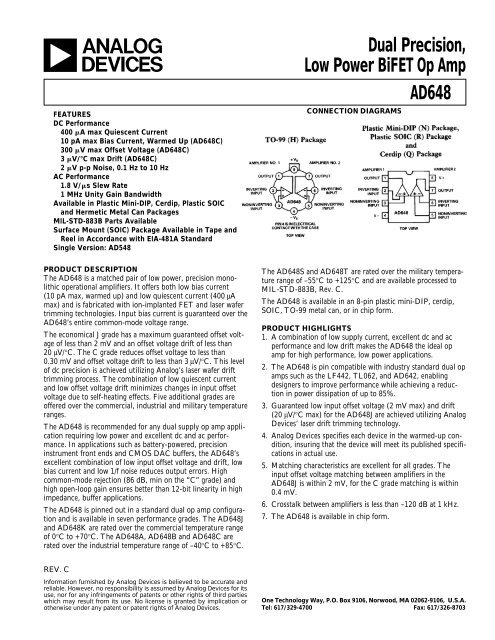
aFEATURESDC Performance400 A max Quiescent Current10 pA max Bias Current, Warmed Up (<strong>AD648</strong>C)300 V max Offset Voltage (<strong>AD648</strong>C)3 V/C max Drift (<strong>AD648</strong>C)2 V p-p Noise, 0.1 Hz to 10 HzAC Performance1.8 V/s Slew Rate1 MHz Unity Gain BandwidthAvailable in Plastic Mini-DIP, Cerdip, Plastic SOICand Hermetic Metal Can PackagesMIL-STD-883B Parts AvailableSurface Mount (SOIC) Package Available in Tape andReel in Accordance with EIA-481A StandardSingle Version: AD548<strong>Dual</strong> <strong>Precision</strong>,<strong>Low</strong> <strong>Power</strong> <strong>BiFET</strong> <strong>Op</strong> <strong>Amp</strong><strong>AD648</strong>CONNECTION DIAGRAMSPRODUCT DESCRIPTIONThe <strong>AD648</strong> is a matched pair of low power, precision monolithicoperational amplifiers. It offers both low bias current(10 pA max, warmed up) and low quiescent current (400 µAmax) and is fabricated with ion-implanted FET and laser wafertrimming technologies. Input bias current is guaranteed over the<strong>AD648</strong>’s entire common-mode voltage range.The economical J grade has a maximum guaranteed offset voltageof less than 2 mV and an offset voltage drift of less than20 µV/°C. The C grade reduces offset voltage to less than0.30 mV and offset voltage drift to less than 3 µV/°C. This levelof dc precision is achieved utilizing Analog’s laser wafer drifttrimming process. The combination of low quiescent currentand low offset voltage drift minimizes changes in input offsetvoltage due to self-heating effects. Five additional grades areoffered over the commercial, industrial and military temperatureranges.The <strong>AD648</strong> is recommended for any dual supply op amp applicationrequiring low power and excellent dc and ac performance.In applications such as battery-powered, precisioninstrument front ends and CMOS DAC buffers, the <strong>AD648</strong>’sexcellent combination of low input offset voltage and drift, lowbias current and low 1/f noise reduces output errors. Highcommon-mode rejection (86 dB, min on the “C” grade) andhigh open-loop gain ensures better than 12-bit linearity in highimpedance, buffer applications.The <strong>AD648</strong> is pinned out in a standard dual op amp configurationand is available in seven performance grades. The <strong>AD648</strong>Jand <strong>AD648</strong>K are rated over the commercial temperature rangeof 0°C to +70°C. The <strong>AD648</strong>A, <strong>AD648</strong>B and <strong>AD648</strong>C arerated over the industrial temperature range of –40°C to +85°C.The <strong>AD648</strong>S and <strong>AD648</strong>T are rated over the military temperaturerange of –55°C to +125°C and are available processed toMIL-STD-883B, Rev. C.The <strong>AD648</strong> is available in an 8-pin plastic mini-DIP, cerdip,SOIC, TO-99 metal can, or in chip form.PRODUCT HIGHLIGHTS1. A combination of low supply current, excellent dc and acperformance and low drift makes the <strong>AD648</strong> the ideal opamp for high performance, low power applications.2. The <strong>AD648</strong> is pin compatible with industry standard dual opamps such as the LF442, TL062, and AD642, enablingdesigners to improve performance while achieving a reductionin power dissipation of up to 85%.3. Guaranteed low input offset voltage (2 mV max) and drift(20 µV/°C max) for the <strong>AD648</strong>J are achieved utilizing AnalogDevices’ laser drift trimming technology.4. Analog Devices specifies each device in the warmed-up condition,insuring that the device will meet its published specificationsin actual use.5. Matching characteristics are excellent for all grades. Theinput offset voltage matching between amplifiers in the<strong>AD648</strong>J is within 2 mV, for the C grade matching is within0.4 mV.6. Crosstalk between amplifiers is less than –120 dB at 1 kHz.7. The <strong>AD648</strong> is available in chip form.REV. CInformation furnished by Analog Devices is believed to be accurate andreliable. However, no responsibility is assumed by Analog Devices for itsuse, nor for any infringements of patents or other rights of third partieswhich may result from its use. No license is granted by implication orotherwise under any patent or patent rights of Analog Devices.One Technology Way, P.O. Box 9106, Norwood, MA 02062-9106, U.S.A.Tel: 617/329-4700 Fax: 617/326-8703
<strong>AD648</strong>–SPECIFICATIONS (@ + 25C and V S = 15 V dc, unless otherwise noted)Model <strong>AD648</strong>J/A/S <strong>AD648</strong>K/B/T <strong>AD648</strong>CMin Typ Max Min Typ Max Min Typ Max UnitsINPUT OFFSET VOLTAGE 1Initial Offset 0.75 2.0 0.3 1.0 0.10 0.3 mVT MIN to T MAX 3.0/3.0/3.0 1.5/1.5/2.0 0.5 mVvs. Temperature 20 10 3.0 µV/°Cvs. Supply 80 86 86 dBvs. Supply, T MIN to T MAX 76/76/76 80 80 dBLong-Term Offset Stability 15 15 15 µV/monthINPUT BIAS CURRENTEither Input, 2 V CM = 0 5 20 3 10 3 10 pAEither Input 2 at T MAX , V CM = 0 0.45/1.3/20 0.25/0.65/10 0.65 nAMax Input Bias Current OverCommon-Mode Voltage Range 30 15 15 pAOffset Current, V CM = 0 5 10 2 5 2 5 pAOffset Current at T MAX 0.25/0.7/10 0.15/0.35/5 0.35 nAMATCHING CHARACTERISTICS 3Input Offset Voltage 1.0 2.0 0.5 1.0 0.2 0.4 mVInput Offset Voltage T MIN to T MAX 3.0/3.0/3.0 1.5/1.5/2.0 0.5 mVInput Offset Voltage vs. Temperature 8 5 2.5 µV/°CInput Bias Current 10 5 5 pACrosstalk –120 –120 –120 dBINPUT IMPEDANCEDifferential 1 × 10 1 2 3 1 × 10 12 3 1 × 10 12 3 ΩpFCommon Mode 3 × 10 12 3 3 × 10 12 3 3 × 10 12 3 ΩpFINPUT VOLTAGE RANGEDifferential 4 ± 20 ± 20 ± 20 VCommon Mode ± 11 ± 12 ± 11 ± 12 ± 11 ± 12 VCommon-Mode RejectionV CM = ± 10 V 76 82 86 dBT MIN to T MAX 76/76/76 82 86 dBV CM = ± 11 V 70 76 76 dBT MIN to T MAX 70/70/70 76 76 dBINPUT VOLTAGE NOISEVoltage 0.1 Hz to 10 Hz 2 2 2 4.0 µV p-pf = 10 Hz 80 80 80 nV/√Hzf = 100 Hz 40 40 40 nV/√Hzf = 1 kHz 30 30 30 nV/√Hzf = 10 kHz 30 30 30 nV/√HzINPUT CURRENT NOISEf = 1 kHz 1.8 1.8 1.8 fA/√HzFREQUENCY RESPONSEUnity Gain, Small Signal 0.8 1.0 0.8 1.0 0.8 1.0 MHzFull <strong>Power</strong> Response 30 30 30 kHzSlew Rate, Unity Gain 1.0 1.8 1.0 1.8 1.0 1.8 V/µsSettling Time to ± 0.01% 8 8 8 µsOPEN-LOOP GAINV O = ±10 V, R L ≥ 10 kΩ 300 1000 300 1000 300 1000 V/mVT MIN to T MAX , R L ≥ 10 kΩ 300/300/300 700 300 700 300 700 V/mVV O = ±10 V, R L ≥ 5 kΩ 150 500 150 500 150 500 V/mVT MIN to T MAX , R L ≥ 5 kΩ 150/150/150 300 150 300 150 300 V/mVOUTPUT CHARACTERISTICSVoltage @ R L ≥ 10 kΩ,T MIN to T MAX ± 12/± 12/±12 ± 13 ± 12 ± 13 ± 12 ± 13 VVoltage @ R L ≥ 5 kΩ,T MIN to T MAX ± 11/± 11/±11 ± 12 ± 11 ± 12 ± 11 ± 12 VShort Circuit Current 15 15 15 mAPOWER SUPPLYRated Performance ± 15 ± 15 ± 15 V<strong>Op</strong>erating Range ± 4.5 ± 18 ± 4.5 ± 18 ± 4.5 ± 18 VQuiescent Current (Both <strong>Amp</strong>lifiers) 340 400 340 400 340 400 µATEMPERATURE RANGE<strong>Op</strong>erating, Rated PerformanceCommercial (0°C to +70°C) <strong>AD648</strong>J <strong>AD648</strong>KIndustrial (–40°C to +85°C) <strong>AD648</strong>A <strong>AD648</strong>B <strong>AD648</strong>CMilitary (–55°C to +125°C) <strong>AD648</strong>S <strong>AD648</strong>TPACKAGE OPTIONSSOIC (R-8) <strong>AD648</strong>JR <strong>AD648</strong>KRPlastic (N-8) <strong>AD648</strong>JN <strong>AD648</strong>KNCerdip (Q-8) <strong>AD648</strong>AQ, <strong>AD648</strong>SQ, <strong>AD648</strong>SQ/883B <strong>AD648</strong>BQ, <strong>AD648</strong>TQ/883B <strong>AD648</strong>CQMetal Can (H-08A) <strong>AD648</strong>AH <strong>AD648</strong>BH, <strong>AD648</strong>TH/883BTape and Reel <strong>AD648</strong>JR-REEL, <strong>AD648</strong>JR-REEL7 <strong>AD648</strong>KR-REEL, <strong>AD648</strong>KR-REEL7Chips Available<strong>AD648</strong>JChips, <strong>AD648</strong>SChips–2– REV. C
NOTES1 Input Offset Voltage specifications are guaranteed after 5 minutes of operation at T A = +25°C.2 Bias Current specifications are guaranteed maximum at either input after 5 minutes of operation at T A = +25°C. For higher temperature, the current doublesevery 10°C.3 Matching is defined as the difference between parameters of the two amplifiers.4 Defined as voltages between inputs, such that neither exceeds ± 10 V from ground.Specifications subject to change without notice.<strong>AD648</strong>ABSOLUTE MAXIMUM RATINGS 1Supply Voltage . . . . . . . . . . . . . . . . . . . . . . . . . . . . . . . . ±18 VInternal <strong>Power</strong> Dissipation 2 . . . . . . . . . . . . . . . . . . . .500 mWInput Voltage 3 . . . . . . . . . . . . . . . . . . . . . . . . . . . . . . . . ±18 VOutput Short Circuit Duration . . . . . . . . . . . . . . . . . IndefiniteDifferential Input Voltage . . . . . . . . . . . . . . . . . . +V S and –V SStorage Temperature Range (Q, H) . . . . . . . . –65°C to +150°CStorage Temperature Range (N, R) . . . . . . . . –65°C to +125°C<strong>Op</strong>erating Temperature Range<strong>AD648</strong>J/K . . . . . . . . . . . . . . . . . . . . . . . . . . . 0°C to +70°C<strong>AD648</strong>A/B/C . . . . . . . . . . . . . . . . . . . . . . . .–40°C to +85°C<strong>AD648</strong>S/T . . . . . . . . . . . . . . . . . . . . . . . . . –55°C to +125°CLead Temperature Range (Soldering 60 sec) . . . . . . . . +300°CNOTES1 Stresses above those listed under “Absolute Maximum Ratings” may causepermanent damage to the device. This is a stress rating only and functionaloperation of the device at these or any other conditions above those indicated in theoperational section of this specification is not implied. Exposure to absolutemaximum rating conditions for extended periods may affect device reliability.2 Thermal Characteristics:8-Pin Plastic Package: θ JA = 165°C/Watt8-Pin Cerdip Package: θ JC = 22°C/Watt; θ JA = 110°C/Watt8-Pin Metal Package: θ JC = 65°C/Watt; θ JA = 150°C/Watt8-Pin SOIC Package: θ JC = 42°C/Wat; θ JA = 160°C/Watt3 For supply voltages less than ±18 V, the absolute maximum input voltage is equalto the supply voltage.METALIZATION PHOTOGRAPHContact factory for latest dimensions.Dimensions shown in inches and (mm).CAUTIONESD (electrostatic discharge) sensitive device. Electrostatic charges as high as 4000 V readilyaccumulate on the human body and test equipment and can discharge without detection.Although the <strong>AD648</strong> features proprietary ESD protection circuitry, permanent damage mayoccur on devices subjected to high energy electrostatic discharges. Therefore, proper ESDprecautions are recommended to avoid performance degradation or loss of functionality.WARNING!ESD SENSITIVE DEVICEREV. C –3–
<strong>AD648</strong>—Typical Characteristics–4–REV. C
REV. C –5–<strong>AD648</strong>
<strong>AD648</strong>APPLICATION NOTESThe <strong>AD648</strong> is a pair of JFET-input op amps with a guaranteedmaximum I B of less than 10 pA, and offset and drift lasertrimmedto 0.3 mV and 3 µV/°C, respectively (<strong>AD648</strong>C). ACspecs include 1 MHz bandwidth, 1.8 V/µs typical slew rate and8 µs settling time for a 20 V step to ±0.01%—all at a supplycurrent less than 400 µA. To capitalize on the device’s performance,a number of error sources should be considered.The minimal power drain and low offset drift of the <strong>AD648</strong> reduceself-heating or “warm-up” effects on input offset voltage,making the <strong>AD648</strong> ideal for on/off battery powered applications.The power dissipation due to the <strong>AD648</strong>’s 400 µA supplycurrent has a negligible effect on input current, but heavy outputloading will raise the chip temperature. Since a JFET’sinput current doubles for every 10°C rise in chip temperature,this can be a noticeable effect.The amplifier is designed to be functional with power supplyvoltages as low as ±4.5 V. It will exhibit a higher input offsetvoltage than at the rated supply voltage of ±15 V, due to powersupply rejection effects. Common-mode range extends from 3 Vmore positive than the negative supply to 1 V more negativethan the positive supply. Designed to cleanly drive up to 10 kΩand 100 pF loads, the <strong>AD648</strong> will drive a 2 kΩ load with reducedopen-loop gain.Figure 21 shows the recommended crosstalk test circuit. A typicalvalue for crosstalk is –120 dB at 1 kHz.Figure 22. Board Layout for Guarding InputsINPUT PROTECTIONThe <strong>AD648</strong> is guaranteed to withstand input voltages equal tothe power supply potential. Exceeding the negative supply voltageon either input will forward bias the substrate junction ofthe chip. The induced current may destroy the amplifier due toexcess heat.Input protection is required in applications such as a flame detectorin a gas chromatograph, where a very high potential maybe applied to the input terminals during a sensor fault condition.Figures 23a and 23b show simple current limiting schemesthat can be used. R PROTECT should be chosen such that themaximum overload current is 1.0 mA (for example 100 kΩ for a100 V overload).Figure 21. Crosstalk Test CircuitLAYOUTTo take full advantage of the <strong>AD648</strong>’s 10 pA max input current,parasitic leakages must be kept below an acceptable level. Thepractical limit of the resistance of epoxy or phenolic circuitboard material is between 1 × 10 12 Ω and 3 × 10 12 Ω. This canresult in an additional leakage of 5 pA between an input of 0 Vand a –15 V supply line. Teflon or a similar low leakage material(with a resistance exceeding 10 17 Ω) should be used to isolatehigh impedance input lines from adjacent lines carrying highvoltages. The insulator should be kept clean, since contaminantswill degrade the surface resistance.A metal guard completely surrounding the high impedancenodes and driven by a voltage near the common-mode inputpotential can also be used to reduce some parasitic leakages.The guarding pattern in Figure 22 will reduce parasitic leakagedue to finite board surface resistance; but it will not compensatefor a low volume resistivity board.Figure 23a. Input Protection of l-to-V ConverterFigure 23b. Voltage Follower Input Protection MethodFigure 23b shows the recommended method for protecting avoltage follower from excessive currents due to high voltagebreakdown. The protection resistor, R P , limits the input current.A nominal value of 100 kΩ will limit the input current to lessthan 1 mA with a 100 volt input voltage applied.The stray capacitance between the summing junction andground will produce a high frequency roll-off with a cornerfrequency equal to:f corner = 12 π R P C strayAccordingly, a 100 kΩ value for R P with a 3 pF C stray will causea 3 dB corner frequency to occur at 531 kHz.–6–REV. C
<strong>AD648</strong>Figure 23c shows a diode clamp protection scheme for an I-to-Vconverter using low leakage diodes. Because the diodes are connectedto the op amp’s summing junction, which is a virtualground, their leakage contribution is minimal.Figure 23c. I-to-V Converter with Diode Input ProtectionExceeding the negative common-mode range on either inputterminal causes a phase reversal at the output, forcing the amplifieroutput to the corresponding high or low state. Exceedingthe negative common mode on both inputs simultaneouslyforces the output high. Exceeding the positive common-moderange on a single input doesn’t cause a phase reversal; but ifboth inputs exceed the limit, the output will be forced high. Inall cases, normal amplifier operation is resumed when inputvoltages are brought back within the common-mode range.D/A CONVERTER BIPOLAR OUTPUT BUFFERThe circuit in Figure 24 provides 4 quadrant multiplication witha resolution of 12 bits. The <strong>AD648</strong> is used to convert the AD7545CMOS DAC’s output current to a voltage and provides thenecessary level shifting to achieve a bipolar voltage output. Thecircuit operates with a 12-bit plus sign input code. The transferfunction is shown in Figure 25.The AD7592 is a fully protected dual CMOS SPDT switch withdata latches. R4 and R5 should match to within 0.01% to maintainthe accuracy of the converter. A mismatch between R4 andR5 introduces a gain error. Overall gain is trimmed by adjustingR IN . The <strong>AD648</strong>’s low input offset voltage, low drift over temperature,and excellent dynamics make it an attractive lowpower output buffer.The input offset voltage of the <strong>AD648</strong> output amplifier resultsin an output error voltage. This error voltage equals the inputoffset voltage of the op amp times the noise gain of the amplifier.That is:V OS Output = V OS Input ⎛1+ R FB ⎞⎝ ⎠R FB is the feedback resistor for the op amp, which is internal tothe DAC. R O is the DAC’s R-2R ladder output resistance. Thevalue of R O is code dependent. This has the effect of changingthe offset error voltage at the amplifier’s output. An output amplifierwith a sub millivolt input offset voltage is needed to preservethe linearity of the DAC’s transfer function.R OFigure 24. 12-Bit Plus Sign Magnitude D/A ConverterSIGN BITBINARY NUMBER IN DAC REGISTER ANALOG OUTPUT0 1111 1111 1111 +V IN (4095/4096)0 0000 0000 0000 0 VOLTS1 0000 0000 0000 0 VOLTS1 1111 1111 1111 –V IN (4095/4096)NOTE: SIGN BIT AT "0" CONNECTS THE NONINVERTING INPUT OFA2 TO ANALOG COMMONFigure 25. Sign Magnitude Code TableREV. C –7–
<strong>AD648</strong>The <strong>AD648</strong> in this configuration provides a 700 kHz small signalbandwidth and 1.8 V/µs typical slew rate. The 33 pF capacitoracross the feedback resistor optimizes the circuit’s response.The oscilloscope photos in Figures 26a and 26b show small andlarge signal outputs of the circuit in Figure 24. Upper tracesshow the input signal V IN . <strong>Low</strong>er traces are the resulting outputvoltage with the DAC’s digital input set to all 1s. The circuitsettles to ±0.01% for a 20 V input step in 14 µs.Figure 26a. Response to ±20 V p-p Reference SquareWaveDUAL PHOTODIODE PREAMPThe performance of the dual photodiode preamp shown in Figure27 is enhanced by the <strong>AD648</strong>’s low input current, inputvoltage offset, and offset voltage drift. Each photodiode sourcesa current proportional to the incident light power on its surface.R F converts the photodiode current to an output voltage equalto R F × I S .An error budget illustrating the importance of low amplifier inputcurrent, voltage offset, and offset voltage drift to minimizeoutput voltage errors can be developed by considering theequivalent circuit for the small (0.2 mm 2 area) photodiodeshown in Figure 27. The input current results in an error proportionalto the feedback resistance used. The amplifier’s offsetwill produce an error proportional to the preamp’s noise gain(1+R F /R SH ), where R SH is the photodiode shunt resistance. Theamplifier’s input current will double with every 10°C rise intemperature, and the photodiode’s shunt resistance halves withevery 10°C rise. The error budget in Figure 28 assumes a roomtemperature photodiode R SH of 500 MΩ, and the maximum inputcurrent and input offset voltage specs of an <strong>AD648</strong>C.The capacitance at the amplifier’s negative input (the sum of thephotodiode’s shunt capacitance, the op amp’s differential inputcapacitance, stray capacitance due to wiring, etc.) will cause arise in the preamp’s noise gain over frequency. This can result inexcess noise over the bandwidth of interest. C F reduces thenoise gain “peaking” at the expense of signal bandwidth.Figure 26b. Response to ±100 mV p-p Reference SquareWaveFigure 27. A <strong>Dual</strong> Photodiode Pre-<strong>Amp</strong>TEMP R SH V OS I BC (M) (V) (1 + R F /R SH ) V OS (pA) I B R F TOTAL–25 15,970 150 151 V 0.30 30 V 181 V0 2,830 225 233 V 2.26 262 V 495 V+25 500 300 360 V 10.00 1.0 mV 1.36 mV+50 88.5 375 800 V 56.6 5.6 mV 6.40 mV+75 15.6 450 3.33 mV 320 32 mV 35.3 mV+85 7.8 480 6.63 mV 640 64 mV 70.6 mVFigure 28. Photodiode Pre-<strong>Amp</strong> Errors Over Temperature–8–REV. C
<strong>AD648</strong>INSTRUMENTATION AMPLIFIERThe <strong>AD648</strong>J’s maximum input current of 20 pA per amplifiermakes it an excellent building block for the high input impedanceinstrumentation amplifier shown in Figure 29. Total currentdrain for this circuit is under 600 µA. This configuration isoptimal for conditioning differential voltages from high impedancesources.The overall gain of the circuit is controlled by R G , resulting inthe following transfer function:V OUT (R3 + R4)= 1+V IN R GGains of 1 to 100 can be accommodated with gain nonlinearitiesof less than 0.01%. The maximum input current is 30 pA overthe common-mode range, with a common-mode impedance ofover 1 × 10 12 Ω. The capacitors C1, C2, C3 and C4 compensatefor peaking in the gain over frequency which is caused by inputcapacitance.To calibrate this circuit, first adjust trimmer R1 for commonmoderejection with +10 volts dc applied to the input pins.Next, adjust R2 for zero offset at V OUT with both inputsgrounded. Trim the circuit a second time for optimalperformance.The –3 dB small signal bandwidth for this low power instrumentationamplifier is 700 kHz for a gain of 1 and 10 kHz for again of 100. The typical output slew rate is 1.8 V/µs.Figure 29. <strong>Low</strong> <strong>Power</strong> Instrumentation <strong>Amp</strong>lifierREV. C –9–
<strong>AD648</strong>LOG RATIO AMPLIFIERLog ratio amplifiers are useful for a variety of signal conditioningapplications, such as linearizing exponential transducer outputsand compressing analog signals having a wide dynamicrange. The <strong>AD648</strong>’s picoamp level input current and low inputoffset voltage make it a good choice for the front-end amplifierof the log ratio circuit shown in Figure 30. This circuit producesan output voltage equal to the log base 10 of the ratio of the inputcurrents I 1 and I 2 . Resistive inputs R1 and R2 are providedfor voltage inputs.Input currents I 1 and I 2 set the collector currents of Q1 and Q2,a matched pair of logging transistors. Voltages at points A and Bare developed according to the following familiar diode equation:V BE = (kT/q) ln (I C /I ES )In this equation, k is Boltzmann’s constant, T is absolute temperature,q is an electron charge, and I ES is the reverse saturationcurrent of the logging transistors. The difference of thesetwo voltages is taken by the subtractor section and scaled by afactor of approximately 16 by resistors R9, R10 and R8. Temperaturecompensation is provided by resistors R8 and R15,which have a positive 3500 ppm/°C temperature coefficient.The transfer function for the output voltage is:V OUT = 1 V log 10 (I 2 /I 1 )Frequency compensation is provided by R11, R12, C1, and C2.Small signal bandwidth is approximately 300 kHz at input currentsabove 100 µA and will proportionally decrease with lowersignal levels. D1, D2, R13, and R14 compensate for the effectsof the two logging transistors’ ohmic emitter resistance.To trim this circuit, set the two input currents to 10 µA and adjustV OUT to zero by adjusting the potentiometer on A3. Thenset I 2 to 1 µA and adjust the scale factor such that the outputvoltage is 1 V by trimming potentiometer R10. Offset adjustmentfor A1 and A2 is provided to increase the accuracy of thevoltage inputs.This circuit ensures a 1% log conformance error over an inputcurrent range of 300 pA to l mA, with low level accuracy limitedby the <strong>AD648</strong>’s input current. The low level input voltage accuracyof this circuit is limited by the input offset voltage and driftof the <strong>AD648</strong>.Figure 30. <strong>Precision</strong> Log Ratio <strong>Amp</strong>lifier–10–REV. C
<strong>AD648</strong>OUTLINE DIMENSIONSDimensions shown in inches and (mm).REV. C –11–
PRINTED IN U.S.A.C1023–5–10/88–12–