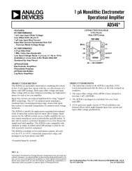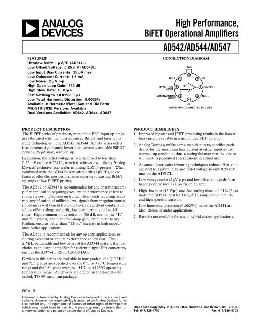
AD542/AD544/AD547 High Performance BiFET ... - ZMiTAC
AD542/AD544/AD547 High Performance BiFET ... - ZMiTAC
AD542/AD544/AD547 High Performance BiFET ... - ZMiTAC

You also want an ePaper? Increase the reach of your titles
YUMPU automatically turns print PDFs into web optimized ePapers that Google loves.
<strong>AD542</strong>/<strong>AD544</strong>/<strong>AD547</strong><strong>AD542</strong> <strong>AD544</strong> <strong>AD547</strong>Parameter Min Typ Max Min Typ Max Min Typ Max UnitsPOWER SUPPLYRated <strong>Performance</strong> ±15 ±15 ±15 VOperating ±5 ±18 ±5 ±18 ±5 ±18 VQuiescent Current 1.1 1.5 1.8 2.5 1.1 1.5 mAVOLTAGE NOISE0.1 Hz to 10 HzJ Grade 2.0 2.0 2.0 µV p-pK, L, S Grades 2.0 2.0 4.0 µV p-p10 Hz 70 35 70 nV/√Hz100 Hz 45 22 45 nV/√Hz1 kHz 30 18 30 nV/√Hz10 kHz 25 16 25 nV/√HzTEMPERATURE RANGEOperating, Rated <strong>Performance</strong>J, K, L Grades 0 to +70 0 to +70 0 to +70 °CS Grade –55 to +125 –55 to +125 –55 to +125 °CStorage –65 to +150 –65 to +150 –65 to +150 °CTRANSISTOR COUNT 29 29 29NOTES1 Open-Loop Gain is specified with V OS both nulled and unnulled.2 Input Offset Voltage specifications are guaranteed after 5 minutes of operation at T A = +25°C.3 Input Offset Voltage Drift is specified with the offset voltage unnulled. Nulling will induce an additional 3 µV/°C/mV of nulled offset.4 Bias Current specifications are guaranteed at either input after 5 minutes of operation at T A = +25°C. For higher temperatures, the current doubles every 10°C.5 Defined as the maximum safe voltage between inputs, such that neither exceeds ± 10 V from ground.Specifications subject to change without notice.Specifications shown in boldface are tested on all production units at final electrical test. Results from those tests are used to calculate outgoing quality levels.All min and max specifications are guaranteed, although only those shown in boldface are tested on all production units.ORDERING GUIDEInitial Offset Settling TimeOffset Voltage to 0.012% for Package PackageModel Voltage Drift a 10 V Step Description Option<strong>AD542</strong>JCHIPS 2.0 mV 20 µV/°C 5 µs Bare Die<strong>AD542</strong>JH 2.0 mV 20 µV/°C 5 µs 8-Pin Hermetic Metal Can H-08A<strong>AD542</strong>KH 1.0 mV 10 µV/°C 5 µs 8-Pin Hermetic Metal Can H-08A<strong>AD542</strong>LH 0.5 mV 5 µV/°C 5 µs 8-Pin Hermetic Metal Can H-08A<strong>AD542</strong>SH 1.0 mV 15 µV/°C 5 µs 8-Pin Hermetic Metal Can H-08A<strong>AD542</strong>SH/883B 1.0 mV 15 µV/°C 5 µs 8-Pin Hermetic Metal Can H-08A<strong>AD544</strong>JH 2.0 mV 20 µV/°C 3 µs 8-Pin Hermetic Metal Can H-08A<strong>AD544</strong>KH 1.0 mV 10 µV/°C 3 µs 8-Pin Hermetic Metal Can H-08A<strong>AD544</strong>LH 0.5 mV 5 µV/°C 3 µs 8-Pin Hermetic Metal Can H-08A<strong>AD544</strong>SH 1.0 mV 15 µV/°C 3 µs 8-Pin Hermetic Metal Can H-08A<strong>AD544</strong>SH/883B 1.0 mV 15 µV/°C 3 µs 8-Pin Hermetic Metal Can H-08A<strong>AD547</strong>JH 1.0 mV 5 µV/°C 5 µs 8-Pin Hermetic Metal Can H-08A<strong>AD547</strong>KH 0.5 mV 2 µV/°C 5 µs 8-Pin Hermetic Metal Can H-08A<strong>AD547</strong>LH 0.25 mV 1 µV/°C 5 µs 8-Pin Hermetic Metal Can H-08A<strong>AD547</strong>SCHIPS 0.5 mV 5 µV/°C 5 µs Bare Die<strong>AD547</strong>SH/883B 0.5 mV 5 µV/°C 5 µs 8-Pin Hermetic Metal Can H-08AREV. B –3–
<strong>AD542</strong>/<strong>AD544</strong>/<strong>AD547</strong>–Typical CharacteristicsFigure 1. Input Voltage Range vs.Supply VoltageFigure 2. Output Voltage Swing vs.Supply VoltageFigure 3. Output Voltage Swing vs.Load ResistanceFigure 4. Input Bias Current vs.Supply VoltageFigure 5. Input Bias Current vs.TemperatureFigure 6. Input Bias Current vs.CMVFigure 7. Change in Offset Voltagevs. Warm-Up TimeFigure 8. Open Loop Gain vs.TemperatureFigure 9. Open Loop FrequencyResponse–4–REV. B
<strong>AD542</strong>/<strong>AD544</strong>/<strong>AD547</strong>Figure 10. Open Loop VoltageGain vs. Supply VoltageFigure 11. Power Supply Rejectionvs. FrequencyFigure 12. Common-Mode RejectionRatio vs. FrequencyFigure 13. Quiescent Current vs.Supply VoltageFigure 14. Large Signal FrequencyResponseFigure 15. <strong>AD544</strong> Output Swing andError vs. Settling TimeFigure 16. <strong>AD544</strong> Total HarmonicDistortion vs. FrequencyFigure 17. Input Noise VoltageSpectral DensityFigure 18. Total RMS Noise vs.Source ResistanceREV. B –5–
<strong>AD542</strong>/<strong>AD544</strong>/<strong>AD547</strong>a. Unity Gain Follower b. Follower with Gain = 10Figure 19. THD Test CircuitsFigure 20. Standard Null CircuitFigure 21a. Unity Gain FollowerPulse Response (Large Signal)Figure 21b. Unity Gain FollowerPulse Response (Small Signal)Figure 21c. Unity Gain Follower–<strong>AD542</strong>/<strong>AD547</strong>Figure 22a. Unity Gain Inverter<strong>AD542</strong>/<strong>AD547</strong>Figure 22b. Unity Gain InverterPulse Response (Large Signal)Figure 22c. Unity Gain InverterPulse Response (Small Signal)–6–REV. B
<strong>AD542</strong>/<strong>AD544</strong>/<strong>AD547</strong>Figure 23a. Unity Gain FollowerPulse Response (Large Signal)Figure 23b. Unity Gain FollowerPulse Response (Small Signal)Figure 23c. Unity Gain FollowerFigure 24a. Unity Gain InverterFigure 24b. Unity Gain InverterPulse Response (Large Signal)Figure 24c. Unity Gain InverterPulse Response (Small Signal)Figure 25. Settling Time Test CircuitThe upper trace of the oscilloscope photograph of Figure 26shows the settling characteristic of the <strong>AD544</strong>. The lower tracerepresents the input to Figure 27. The <strong>AD544</strong> has been designedfor fast settling to 0.01%, however, feedback components, circuitlayout and circuit design must be carefully considered toobtain optimum settling time.Figure 27. Circuit for Driving a Large Capacitance LoadThe circuit in Figure 27 employs a 100 Ω isolation resistorwhich enables the amplifier to drive capacitance loads exceeding500 pF; the resistor effectively isolates the high frequency feedbackfrom the load and stabilizes the circuit. Low frequencyfeedback is returned to the amplifier summing junction via thelow-pass filter formed by the 100 Ω series resistor and the loadcapacitance, C L .Figure 26. Settling Characteristic Detail–<strong>AD544</strong>Figure 28. Transient Response R L = 2 kΩC L = 500 pF–<strong>AD544</strong>REV. B –7–
<strong>AD542</strong>/<strong>AD544</strong>/<strong>AD547</strong><strong>BiFET</strong> Application HintsAPPLICATION NOTESThe <strong>BiFET</strong> series was designed for high performance op ampapplications that require true dc precision. To capitalize on allof the performance available from the <strong>BiFET</strong>s there are somepractical error sources that should be considered.The bias currents of JFET input amplifiers double with every10°C increase in chip temperature. Therefore, minimizing thejunction temperature of the chip will result in extending theperformance limits of the device.1. Heat dissipation due to power consumption is the maincontributor to self-heating and can be minimized by reducingthe power supplies to the lowest level allowed by theapplication.2. The effects of output loading should be carefully considered.Greater power dissipation increases bias currents and decreasesopen loop gain.GUARDINGThe low input bias current (25 pA) and low noise characteristicsof the high performance <strong>BiFET</strong> op amp make it suitable forelectrometer applications such as photo diode preamplifiers andpicoampere current-to-voltage converters. The use of guardingtechniques in printed circuit board layout and construction iscritical for achieving the ultimate in low leakage performanceavailable from these amplifiers. The input guarding schemeshown in Figure 29 will minimize leakage as much as possible;the guard ring is connected to a low impedance potential at thesame level as the inputs. <strong>High</strong> impedance signal lines should notbe extended for any unnecessary length on a printed circuit.Figure 29. Board Layout for Guarding InputsINPUT PROTECTIONThe <strong>BiFET</strong> series is guaranteed for a maximum safe inputpotential equal to the power supply potential. The input stagedesign also allows differential input voltages of up to ±1 voltwhile maintaining the full differential input resistance of 10 12 Ω.This makes the <strong>BiFET</strong> series suitable for comparator situationsemploying a direct connection to high impedance source.Many instrumentation situations, such as flame detectors in gaschromatographs, involve measurement of low level currentsfrom high-voltage sources. In such applications, a sensor faultcondition may apply a very high potential to the input of thecurrent-to-voltage converting amplifier. This possibility necessitatessome form of input protection. Many electrometer typedevices, especially CMOS designs, can require elaborate Zenerprotection schemes which often compromise overall performance.The <strong>BiFET</strong> series requires input protection only if thesource is not current-limited, and as such is similar to manyJFET-input designs. The failure mode would be overheatingfrom excess current rather than voltage breakdown. If thesource is not current-limited, all that is required is a resistor inseries with the affected input terminal so that the maximumoverload current is 1.0 mA (for example, 100 kΩ for a 100 voltoverload). This simple scheme will cause no significant reductionin performance and give complete overload protection. Figure30 shows proper connections.Figure 30. Input ProtectionD/A CONVERTER APPLICATIONSThe <strong>BiFET</strong> series of operational amplifiers can be used withCMOS DACs to perform both 2-quadrant and 4-quadrantoperation. The output impedance of a CMOS DAC varies withthe digital word, thus changing the noise gain of the amplifiercircuit. The effect will cause a nonlinearity the magnitude ofwhich is dependent on the offset voltage of the amplifier. The<strong>BiFET</strong> series with trimmed offset will minimize this effect. Additionally,the Schottky protection diodes recommended for usewith many older CMOS DACs are not required when using oneof the <strong>BiFET</strong> series amplifiers.Figure 31a shows the <strong>AD547</strong> and AD7541 configured for unipolarbinary (2-quadrant multiplication) operation. With a dcreference voltage or current (positive or negative polarity) appliedat pin 17, the circuit operates as a unipolar converter.With an ac reference voltage or current, the circuit provides2-quadrant multiplication (digitally controlled attenuation).Figure 31a. <strong>AD547</strong> Used as DAC Output Amplifier–8–REV. B
<strong>AD542</strong>/<strong>AD544</strong>/<strong>AD547</strong>The oscilloscope photo of Figure 31b shows the output of thecircuit of Figure 31a. The upper trace represents the referenceinput, and the bottom trace shows the output voltage for adigital input of all ones on the DAC (Gain 1–2 –n ). The 47 pFcapacitor across the feedback resistor compensates for the DACoutput capacitance, and the 150 pF load capacitor serves tominimize output glitches.USING THE <strong>AD547</strong> IN LOG AMPLIFIER APPLICATIONSLog amplifiers or log ratio amplifiers are useful in applicationsrequiring compression of wide-range analog input data, linearizationof transducers having exponential outputs, and analogcomputing, ranging from simple translation of natural relationshipsin log form (e.g., computing absorbance as the log-ratio ofinput currents), to the use of logarithms in facilitating analogcomputation of terms involving arbitrary exponents andmulti-term products and ratios.The picoamp level input current and low offset voltage of the<strong>AD547</strong> make it suitable for wide dynamic range log amplifiers.Figure 33 is a schematic of a log ratio circuit employing the<strong>AD547</strong> that can achieve less than 1% conformance error over 5decades of current input, 1 nA to 100 µA. For voltage inputs,the dynamic range is typically 50 mV to 10 V for 1% error,limited on the low end by the amplifiers’ input offset voltage.Figure 31b. Voltage Output DAC Settling CharacteristicFigure 32a illustrates the 10-bit digital-to-analog converter,AD7533, connected for bipolar operation. Since the digitalinput can accept bipolar numbers and V REF can accept a bipolaranalog input, the circuit can perform a 4-quadrant multiplyingfunction.Figure 32a. <strong>AD544</strong> Used as DAC Output AmplifiersThe photos exhibit the response to a step input at V REF . Figure32b is the large signal response and Figure 32c is the small signalresponse. C1 phase compensation (15 pF) is required forstability when using high speed amplifiers. C1 is used to cancelthe pole formed by the DAC internal feedback resistance andthe output capacitance of the DAC.Figure 33. Log-Ratio AmplifierThe conversion between current (or voltage) input and log outputis accomplished by the base emitter junctions of the dualtransistor Q1. Assuming Q1 has β > 100, which is the case forthe specified transistor, the base-emitter voltage on side 1 is to aclose approximation:V BE A = kT/q ln I 1 /I S1This circuit is arranged to take the difference of the V BE ’s ofQ1A and Q1B, thus producing an output voltage proportionalto the log of the ratio of the inputs:V OUT= – K (V BE A– V BE B) = – KkTq(ln I 1/I S1–lnI 2/I S2)Figure 32b. Large SignalResponseFigure 32c. Small SignalResponseV OUT=−KkT/qln I 1/I 2The scaling constant, K is set by R1 and R TC to about 16, toproduce 1 V change in output voltage per decade difference ininput signals. R TC is a special resistor with a +3500 ppm/°Ctemperature coefficient, which makes K inversely proportionalto temperature, compensating for the “T” in kT/q. The logratiotransfer characteristic is therefore independent oftemperature.REV. B –9–
<strong>AD542</strong>/<strong>AD544</strong>/<strong>AD547</strong>This particular log ratio circuit is free from the dynamic problemsthat plague many other log circuits. The –3 dB bandwidthis 50 kHz over the top 3 decades, 100 nA to 100 µA, and decreasessmoothly at lower input levels. This circuit needs no additionalfrequency compensation for stable operation frominput current sources, such as photodiodes, that may have 100pF of shunt capacitance. For larger input capacitances a 20 pFintegration capacitor around each amplifier will provide asmoother frequency response.This log ratio amplifier can be readily adjusted for optimumaccuracy by following this simple procedure. First, apply V1 =V2 = –10.00 V and adjust “Balance” for V OUT = 0.00 V. Nextapply V1 = –10.00 V, V2 = –1.00 V and adjust gain for V OUT =+1.00 V. Repeat this procedure until gain and balance readingsare within 2 mV of ideal values.Figure 34. DifferentiatorFigure 35. Low Drift Integrator andLow Leakage Guarded ResetFigure 36. Wien-BridgeOscillator–f O = 10 kHzFigure 37. CapacitanceMultiplierFigure 38. Long IntervalTimer–1,000 SecondsFigure 39. Positive Peak Detector–10–REV. B
<strong>AD542</strong>/<strong>AD544</strong>/<strong>AD547</strong>OUTLINE DIMENSIONSDimensions shown in inches and (mm).TO-99 (H-08A)REV. B –11–
–12–PRINTED IN U.S.A. C826c–2–11/91