AD1B60 Intelligent Digitizing Signal Conditioner - ZMiTAC
AD1B60 Intelligent Digitizing Signal Conditioner - ZMiTAC
AD1B60 Intelligent Digitizing Signal Conditioner - ZMiTAC

Create successful ePaper yourself
Turn your PDF publications into a flip-book with our unique Google optimized e-Paper software.
<strong>AD1B60</strong>–SPECIFICATIONS(@ T A = –25C to +85C and power supplies of 5 V 5%, unless otherwise noted)<strong>AD1B60</strong>BS, <strong>AD1B60</strong>BJParameter Min Typ Max Unit NotesACCURACY (ERROR)Range 0 (±10 mV) ±0.06 ±0.11 % FSR Notes 1 and 2 (All Ranges); at +25°CRange 1 (±20 mV) ±0.03 ±0.06 % FSRRange 2 (±50 mV) ±0.015 ±0.03 % FSRRange 3 (±100 mV) ±0.008 ±0.015 % FSRRange 4 (±200 mV) ±0.005 ±0.008 % FSRRange 5 (±500 mV) ±0.005 ±0.007 % FSRRange 6 (±1 V) ±0.005 ±0.007 % FSRRange 7 (±2 V) ±0.005 ±0.007 % FSRRange 8 (±5 V) ±0.007 ±0.010 % FSRRange 9 (±10 V) ±0.005 ±0.010 % FSRRange A (Type J, 0°C to 760°C) ±0.25 ±0.45 °C Note 3 (Temperature Ranges)Range B (Type K, 0°C to 1000°C) ±0.55 ±0.75 °CRange C (Type T, –100°C to +400°C) ±0.25 ±0.45 °CRange D (Type E, 0°C to 1000°C) ±0.20 ±0.35 °CRange E (Type R, 500°C to 1750°C) ±1.00 ±1.75 °CRange F (Type S, 500°C to 1750°C) ±1.15 ±2.05 °CRange 10 (Type B, 500°C to 1800°C) ±1.15 ±2.15 °CRange 11 (Pt 385, –200°C to 800°C) ±0.20 ±0.40 °CRange 12 (Pt 392, –200°C to 800°C) ±0.20 ±0.40 °CACCURACY (ERROR) DRIFTRange 0 (±10 mV) –40 –100 ppm/°C Notes 4 and 5 (All Ranges)Range 1 (±20 mV) –20 ppm/°CRange 2 (±50 mV) –10 ppm/°CRange 3 (±100 mV) –5 ppm/°CRange 4 (±200 mV) –5 ppm/°CRange 5 (±500 mV) –5 ppm/°CRange 6 (±1 V) –5 ppm/°CRange 7 (±2 V) –5 ppm/°CRange 8 (±5 V) –5 ppm/°CRange 9 (±10 V) –5 ppm/°CRange A (Type J, 0°C to 760°C) –10 ppm/°CRange B (Type K, 0°C to 1000°C) –10 ppm/°CRange C (Type T, –100°C to +400°C) –20 ppm/°CRange D (Type E, 0°C to 1000°C) –10 ppm/°CRange E (Type R, 500°C to 1750°C) –20 ppm/°CRange F (Type S, 500°C to 1750°C) –40 ppm/°CRange 10 (Type B, 500°C to 1800°C) –40 ppm/°CRange 11 (Pt 385, –200°C to 800°C) ±10 ±25 ppm/°C Note 6 (RTD Ranges)Range 12 (Pt 392, –200°C to 800°C) ±10 ±25 ppm/°CRESOLUTIONRange 0 (±10 mV) ±0.035 % FSR Notes 2 and 5 (All Ranges)Range 1 (±20 mV) ±0.02 % FSRRange 2 (±50 mV) ±0.01 % FSRRange 3 (±100 mV) ±0.004 % FSRRange 4 (±200 mV) ±0.002 % FSRRange 5 (±500 mV) ±0.0015 % FSRRange 6 (±1 V) ±0.0015 % FSRRange 7 (±2 V) ±0.0015 % FSRRange 8 (±5 V) ±0.0015 % FSRRange 9 (±10 V) ±0.0015 % FSRRange A (Type J, 0°C to 760°C) ±0.15 °CRange B (Type K, 0°C to 1000°C) ±0.2 °CRange C (Type T, –100°C to +400°C) ±0.15 °CRange D (Type E, 0°C to 1000°C) ±0.1 °CRange E (Type R, 500°C to 1750°C) ±0.55 °CRange F (Type S, 500°C to 1750°C) ±0.6 °CRange 10 (Type B, 500°C to 1800°C) ±0.7 °CRange 11 (Pt 385, –200°C to +800°C) ±0.15 °CRange 12 (Pt 392, –200°C to +800°C) ±0.15 °C–2–REV. A
<strong>AD1B60</strong><strong>AD1B60</strong>BS, <strong>AD1B60</strong>BJParameter Min Typ Max Unit NotesINPUT CHARACTERISTICSNormal Mode Rejection (@ 50 Hz or 60 Hz) 66 dB At Integration Time ≥ 100 ms50 dB Note 2Input Bias Current –0.5 –3 nA At T A = +25°C–0.5 nA At –25°C ≤ T A ≤ +85°CInput ImpedanceChannel 0-3 10 MΩAttenuator Input 35 50 65 kΩRTD & THERMOCOUPLE CHANNELSRTD Excitation Current Output (EXCIT) –150 –200 –250 µA Note 7; at T A = +25°Cvs. Temperature ±75 ±300 ppm/°C Note 6Open Thermocouple Detection Current (EXCIT) –10 nACJC Excitation Current Output (CJC) –15 –20 –25 µA Note 8; at T A = +25°CREFERENCEInternal Reference Output Voltage 2.360 2.500 2.640 Vvs. Temperature ±25 ±50 ppm/°CInternal Reference Voltage Noise 0.01 % p-pRef In Current 350 µATIMINGConversion Throughput Rate 2.5 100 conv/sec Note 9Integration Time (User Configurable) 2 200 ms See Table IVIntegration Capacitor 1 2.2 3 nF Note 10Oscillator Frequency 11.0592 MHz Notes 10 and 11Integration Latency 100 µs See Figure 2BCLK-to-DATA Delay, Synchronous Port 30 ns See Figure 4Minimum CS High Time 400 µs See Figure 4Reset Input Pulse Width (RESETI) 5 µsDIGITAL LEVELSAt +25°CInputsLogic 0 Voltage 0.8 VLogic 1 Voltage (Except RESETI) 2.0 VLogic 1 Voltage (RESETI) 0.7* (+5VDIG) + 0.1 VOutputsLogic 0 Voltage (I SlNK = 1.6 mA) 0.45 VLogic 1 Voltage (I SOURCE = –60 µA) 2.4 VInput Current (CC, RXD, CH/BR0-1, ACM, PMODE)Logic 0 –75 µA At V IN = 0.45 VLogic 1-to-0 Transition –750 µA At V IN = 2.0 VInput Current (R/ADD0-4, CLK, CS) ±10 µA At 0.45 ≤ V lN ≤ +5VDIGInput Pulldown Resistor (RESETI) 50 150 kΩPOWER REQUIREMENTSAt +25°C+V Analog (+5VANA) 4.75 5.00 5.25 V7 15 mA At +5VANA = 5.0 V–V Analog (–5VANA) –5.25 –5.00 –4.75 V–7 –15 mA At –5VANA = –5.0 V+V Digital (+5VDIG) 4.75 5.00 5.25 V Note 1210 30 mA At +5VDIG = 5.0 VPower Supply Rejection Ratio –70 dBBROWNOUT DETECTOR±V Analog Threshold ±3.9 V+V Digital Threshold 3.5 VTEMPERATURE RANGERated Performance –25 +85 °COperating –40 +85 °CStorage –40 +85 °CREV. A –3–
<strong>AD1B60</strong>NOTES1 Accuracy specifications include factory calibration errors but do not include reference noise. Also, accuracy specifications for thermocouple ranges do not includeCJC calculation errors, which depend on the calculation method chosen. To calculate total measurement error, add reference noise expressed as a percentage of thereference voltage to the specified accuracy error. Because reference noise results in a gain error, its effect is a percentage of reading. For example, a measurementmade using the ± 1 V input range and a reference with ± 0.01% maximum noise would have a maximum error of ±0.007% FSR ± 0.01% of reading. FSR = Full-ScaleRange, i.e., span of input values. For thermocouple ranges, also add to the measurement error the values in Table A corresponding to the selected CJC type. For example,a measurement made with a Type J thermocouple, downloaded CJC temperature, and a reference with ± 0.01% maximum noise would have a maximum errorof ± 0.456°C ± 0.01% of reading.2 At integration time ≤ 33.3 ms and equal to an integral number of power-line cycles.3 Temperature ranges use the International Practical Temperature Scale of 1968 (IPTS-68). Thermocouple accuracy specifies conformance to NIST Monograph 125.RTD accuracy specifies conformance to JIS C 1604, DIN 43760, and IEC 751.4 Errors expressed as ppm (parts per million) of reading.5 Excluding reference noise and drift.6 RTD measurement drift is digitally compensated to 25 ppm/°C of reading (maximum), including effects of reference, excitation current, and gain drift.7 RTD measurement accuracy is digitally compensated to values shown on first page of specification table.8 CJC excitation current is enabled only when the “Thermistor” CJC mode is selected; see Table V.9 Minimum throughput occurs at T INT = 200 ms for any range selection. Maximum throughput occurs at T INT = 2 ms for voltage ranges (ranges 0 through 9) only; seeTable IV.10 User-supplied.11 Specified performance obtained with frequency of 11.0592 MHz ± 0.1%.12 –0.2 V < (+5VANA – +5VDIG) < 0.5 V for specified performance.13 Typical values are not tested or guaranteed. Operation which is specified without explicit reference to variation in operating conditions may differ as these conditionsare altered.Table A. Maximum Thermocouple CJC Calculation ErrorCJC Calculation Thermistor 1 mV/K Downloaded DisabledCJC Mode 00 01 10 11Thermocouple Ambient Temperature of <strong>AD1B60</strong>Type –25C to +85C 25C –25C to +85C 25C –25C to +85C –25C to +85CJ 0.6°C 0.1°C 0.4°C 0.3°C 0.006°C 0°CK 0.6°C 0.1°C 0.4°C 0.3°C 0.012°C 0°CT 0.8°C 0.2°C 0.6°C 0.4°C 0.028°C 0°CE 0.6°C 0.1°C 0.4°C 0.3°C 0.024°C 0°CR 0.4°C 0.1°C 0.3°C 0.2°C 0.007°C 0°CS 0.4°C 0.1°C 0.3°C 0.2°C 0.007°C 0°CB 0.3°C 0.3°C 0.3°C 0.3°C 0.250°C 0°CABSOLUTE MAXIMUM RATINGS*(T A = +25°C unless otherwise stated)+5VDIG to DGND . . . . . . . . . . . . . . . . . . . . . . –0.3 V to +6 V+5VANA to AGND . . . . . . . . . . . . . . . . . . . . . . –0.3 V to +6 V–5VANA to AGND . . . . . . . . . . . . . . . . . . . . . . –6 V to +0.3 V+5VDIG to +5VANA . . . . . . . . . . . . . . . . . . . .–6 V to +0.3 V+5VANA to –5VANA . . . . . . . . . . . . . . . . . . . . . . 0 V to 12 VAGND to DGND . . . . . . . . . . . . . . . . . . . . . . . . . . . . . ±0.3 VAnalog Inputs to AGND (Exc. ATTEN) . . ±5VANA ± 0.3 VATTEN Input to AGND . . . . . . . . . . . . . . . . . . . . . . . . ±15 VREFOUT, EXCIT to AGND . . –0.3 V to +5VANA + 0.3 VDigital Inputs to DGND . . . . . . . . –0.3 V to +5VDIG + 0.3 VDigital Outputs to DGND . . . . . . . –0.3 V to +5VDIG + 0.3 VStorage Temperature Range . . . . . . . . . . . . –65°C to +150°CLead Temperature (Soldering, 10 sec) . . . . . . . . . . . . . . 300°CPower Dissipation to +75°C . . . . . . . . . . . . . . . . . . 1,000 mWDerate Above +75°C by . . . . . . . . . . . . . . . . . . . . 10 mW/°C*Stresses above those listed under “Absolute Maximum Ratings” may causepermanent damage to the device. These are stress ratings only and functionaloperation of the device at these or any other conditions above those listed in theoperational sections of this specification is not implied. Exposure to absolutemaximum rating conditions for extended periods may affect device reliability.Absolute Maximum Ratings apply individually only, not in combination.ORDERING GUIDEModel Temperature Range Package Option*<strong>AD1B60</strong>BS –40°C to +85°C S-64<strong>AD1B60</strong>BJ –40°C to +85°C J-44<strong>AD1B60</strong>/EB –40°C to +85°C Printed Circuit BoardNOTES*S = Plastic Quad Flatpack (PQFP), J = J-leaded Ceramic Chip Carrier,/EB = Evaluation Board with <strong>AD1B60</strong>BJ & Software. Consult factory foravailability.CAUTIONESD (electrostatic discharge) sensitive device. Electrostatic charges as high as 4000 V readilyaccumulate on the human body and test equipment and can discharge without detection.Although the <strong>AD1B60</strong> features proprietary ESD protection circuitry, permanent damage mayoccur on devices subjected to high energy electrostatic discharges. Therefore, proper ESDprecautions are recommended to avoid performance degradation or loss of functionality.WARNING!ESD SENSITIVE DEVICE–4– REV. A
13 24 REFOUT Output from internal reference (+2.5 V).14 25 REFIN Reference input; may be connecteddirectly to REFOUT.15 26 –5VANA –5 V, ± 5% analog power supply.16 27 AGND Analog ground.17 28 ATTEN 5:1 attenuator input for ± 5 V and ± 10 Vinput voltages.21 29 C2 External integration capacitor (nominally2.2 nF).22 30 C1 External integration capacitor.23 31 NC Make no connection (factory test).24 32 CJC External CJC sensor input. Also outputs20 µA excitation current in thermistorCJC mode.25 33 EXCIT Excitation Output: provides 10 nA foropen thermocouple detection if a thermocouplerange is selected, or 200 µA excitationif an RTD range is selected.26 34 GNDSNS Sense input for ground potential. Connectto AGND (typical).27 35 CH3 Channel 3 signal input.28 36 CH2 Channel 2 signal input.29 37 CH1 Channel 1 signal input.30 38 CH0 Channel 0 signal input.31 39 NC Make no connection (factory test).34 40 RESETO Output from the power-on reset/brownoutdetect/watchdog timer circuit; active high.Connect to RESETI.35 41 +5VDIG +5 V, ± 5% digital power supply; connectalso to other +5 VDIG pins.36 42 CS Chip select input (low to select). Connectto DGND if not used.37 43 CLK Synchronous serial shift clock input. Connectto DGND if not used.38 44 DATA Synchronous serial data output.<strong>AD1B60</strong>Table I. Pin FunctionsBS# BJ# Name ConnectionBS# BJ# Name Connection4 18 RESETI Reset input; active high. Initializes the 39 1 XTLOUT External crystal (11.0592 MHz).<strong>AD1B60</strong> to the pin-strapped and40 2 XTLIN External crystal (11.0592 MHz) or externallogic-level clock input.EEPROM default values. Connect toRESETO.5 19 RXD Receive data input for asynchronous port.41 3 +5VANA +5 V, ± 5% analog power supply.45, 46 4, 5 CH/BR0-1 Channel select inputs when PMODE is6 20 TXD Transmit data output for asynchronouslow at reset. Baud rate select inputs whenport.PMODE is high at reset.7 21 CC Continuous Conversion input. Enables47 6 +5VDIG +5 V, ± 5% digital power supply; connectsynchronous signal integration or continuousconversion. While low, the <strong>AD1B60</strong>also to other +5 VDIG pins.waits in “idle mode.” When CC goes high,the <strong>AD1B60</strong> starts converting. While heldhigh, the <strong>AD1B60</strong> continuously convertsinput data.53–57 7–11 R/ADD4-0 Range select inputs if PMODE is low atreset. Address select inputs if PMODE andACM are high at reset. External pull-upsare required.8 22 DGND Digital ground.58 12 +5VDIG +5 V, ± 5% digital power supply; connect12 23 +5VANA +5 V, ± 5% analog power supply.also to other +5 VDIG pins.59 13 STATUS Computation status output. If Status ishigh, results from the previous signal integrationare being computed; if STATUS islow, results are available.60 14 PMODE Mode select input for CH/BR and R/ADDRpins; high or low state sensed at power-upand reset. Specifies whether input range,input channel, device address, and baudrate are determined by external pins or byvalues in EEPROM.61 15 ACM Addressed Communication Mode input.When ACM is high, address and CRC areenabled.62 16 RDY Ready (integration status) output. If RDYis high, the <strong>AD1B60</strong> is integrating the signal;if RDY is low, the <strong>AD1B60</strong> is integratinga background input.63 17 NC Make no connection (factory test).R/ADD4R/ADD3R/ADD2R/ADD1R/ADD0+5VDIGSTATUSPMODEACMRDYNCNC = NO CONNECT52535455565758596061626364+5VDIGCH/BR1CH/BR0RESETIRXDTXDCCDGND+5VANAXTLINXTLOUTDATACLKCS+5VDIGRESETO51 50 49 48 47 46 45 44 43 42 41 40 39 38 37 36 35 34 33<strong>AD1B60</strong>BSSTOP TOP VIEW(Not to Scale)1 2 3 4 5 6 7 8 9 10 11 12 13 14 15 16 17 18 19NOTES:PIN 23, 31, 63 – DO NOT CONNECT.PINS WITHOUT LABELS ARE NOT INTERNALLY CONNECTED.+5VANAREFOUTREFIN–5VANAAGNDATTEN<strong>AD1B60</strong> Pin Assignments3231 NC30 CH029 CH128 CH227 CH326 GNDSNS25 EXCIT24 CJC23 NC22 C121 C220REV. A–5–
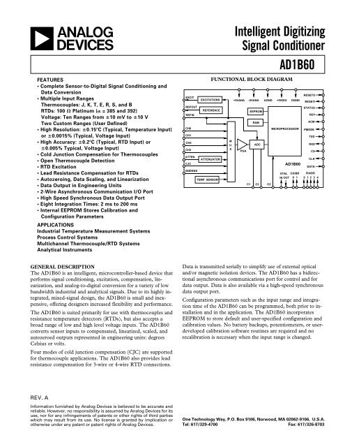
<strong>AD1B60</strong>+5VANA –5VANA AGND +5VDIG DGND NC (TEST)12 41 15 16 35 47 58 8 23 31 63EXCIT25EXCITATIONSREFOUTREFIN1314REFERENCE<strong>AD1B60</strong>BROWNOUT/WATCHDOG344RESETORESETICH0CH1CH2CH3ATTENCJCGNDSNS30292827172426ATTENUATORTEMP. SENSORMUXPGAADCEEPROMRAMMICROPROCESSOR5962616065363738STATUSRDYACMPMODETXDRXDCSCLKDATA22 21 7 40 39 45 46 57 56 55 54 53C1 C2 CC IN OUT 0 1 0 1 2 3 4XTL CH/BRR/ADDFigure 1. Functional Block DiagramFUNCTIONAL DESCRIPTIONThe <strong>AD1B60</strong> is a complete data acquisition subsystem in asingle package which interfaces directly to a sensor and a hostprocessor (see Figure 1). The sensor is applied to one or moreof the multiplexer inputs and amplified by the programmablegain amplifier. Excitation currents for RTDs, open thermocoupleinput detection, and cold junction compensation sensorsare provided.The <strong>AD1B60</strong> has an input multiplexer with four channels forlow level input signals and one channel with an attenuator forhigh level inputs. There are also reference and zero inputs, acold junction compensation channel, and an internal temperaturesense channel on the multiplexer. Voltage input ranges are±10 mV full scale to ±10 V full scale.The multiplexer feeds a programmable gain amplifier (PGA),which has a gain range of 1 to 128. The output of the PGA isapplied to an integrating voltage-to-frequency converter, whichis resolved by the microprocessor. The microprocessor controlsthe input multiplexer and PGA alternately selecting an inputchannel, voltage reference, ground, or other signal channel necessaryfor an accurate measurement.For a voltage measurement, the <strong>AD1B60</strong> will measure the inputvoltage, measurement ground and reference voltage, and willcalculate the value of the input voltage ratiometrically to the referenceand then generate an output value in volts.For thermocouple measurements, the <strong>AD1B60</strong> will also read acold junction sensor, calculate the required CJC correction voltage,apply it to the voltage reading of the thermocouple, andgenerate an output in degrees Celsius.For RTD measurements, the <strong>AD1B60</strong> will perform 3- or 4-wirelead resistance compensation, compensate for internal excitationand gain drifts and generate an output in degrees Celsius.The <strong>AD1B60</strong>s standard input ranges include the seven NISTthermocouple standards, two platinum RTD ranges, and tenvoltage ranges.In addition, the <strong>AD1B60</strong> can use two ranges stored in internalEEPROM. These “custom” ranges are easily created by the userthrough use of the <strong>AD1B60</strong> Custom Range Generation Softwareincluded with every Evaluation Board. Several example files, suchas a Type N thermocouple range, are also included with thesoftware.With each conversion, the <strong>AD1B60</strong> reports status information,input channel, and an overflow flag. The <strong>AD1B60</strong> communicatesvia one or both of its serial ports: a 2-wire asynchronousI/O port up to 19.2 kbaud, and a 3-wire synchronous data outputport up to 5 MBPS.The <strong>AD1B60</strong> contains a brownout detector and watchdogmonitor circuit. If any of the power supplies falls below a threshold,or if the internal microprocessor fails to trigger the watchdogtimer, this circuit will generate a reset output.CONFIGURABLE PARAMETERSYou can set the following parameters of the <strong>AD1B60</strong>:• Device Address• Baud Rate• Channel Selection• Input Range• Integration Time• Cold Junction Compensation Mode• RTD Connection ModeDepending on the parameter, you can change values in the followingways:• Execute <strong>AD1B60</strong> commands to change values in EEPROM.• Set specified pins on the <strong>AD1B60</strong>.• Execute <strong>AD1B60</strong> commands to change values in RAM.–6– REV. A
The factory-programmed default values of the configurable parametersare listed in Table II.If the default values for the device address and baud rate do notmatch those in your application, you must reset the <strong>AD1B60</strong>with the PMODE pin high and the desired device address andbaud rate set by <strong>AD1B60</strong> pins. Using <strong>AD1B60</strong> commands, youcan change the EEPROM-based defaults, and then power upthe <strong>AD1B60</strong> with PMODE low to use the new default valuesfrom EEPROM.The following section describes the configurable parameters.The COMMAND SET section describes the commands used tochange parameter settings.Table II. Configurable Parameters and their Default ValuesConfigurable Factory Default For Details,Parameter Value SeeDevice Address 0 Table IBaud Rate 9600 Table VIIChannel Selection 0 Figure 5Input Range Type J Thermocouple Table IIIIntegration Time 100 ms Table IVCold Junction Com- Direct Connection Table Vpensation Mode of a ThermistorRTD Connection Mode 3-Wire Figure 6CONFIGURATION PARAMETER DESCRIPTIONSDevice AddressIn Addressed Communication Mode (ACM pin high), you canconnect a cluster of up to 32 <strong>AD1B60</strong>s to a single communicationport. Each <strong>AD1B60</strong> in a cluster must have a unique addressfrom 0 to 31 (0 to 1F hex).When the <strong>AD1B60</strong> is reset with PMODE high, the address isread from (R/ADD 4-0). Refer to Table I for more informationon using the pins of the <strong>AD1B60</strong>.When the <strong>AD1B60</strong> is reset with PMODE low, the address isread from EEPROM. You can change the default address storedin EEPROM by executing the WR_EPM_PARS command.Baud RateYou can set one of the following baud rates for the <strong>AD1B60</strong>:2400, 4800, 9600 (the factory default), or 19200.When the <strong>AD1B60</strong> is reset with PMODE low, the baud rate isread from EEPROM. You can change the default baud rate storedin EEPROM by executing the WR_EPM_PARS command.When the <strong>AD1B60</strong> is reset with PMODE high, the baud rate isread from the CH/BR 0-1 pins.Channel SelectionAlthough the <strong>AD1B60</strong> is optimized for single-channel applications,you can use up to five input channels on one device. The<strong>AD1B60</strong> checks the input channel selection before each conversion.Note that selecting an RTD or high voltage input rangealso determines the channel(s).If the <strong>AD1B60</strong> is powered up with PMODE high, Channel 0 isselected. For thermocouple and low level voltage ranges, youcan select an input channel using the SEL_CH command.Check the channel address in the ADSTAT byte returned withthe data to ensure that the data represents the correct channel.REV. A–7–<strong>AD1B60</strong>Also check ADSTAT’s Valid Data flag after changing channels.You may have to wait up to two integration times for valid datawhen changing channels on the same input range. Refer to theCOMMAND SET section for more information on SEL_CH.If the <strong>AD1B60</strong> is reset with PMODE low, the input channel isdetermined by the CH/BR 0-1 pins.Input RangesThe <strong>AD1B60</strong> supports the input ranges listed in Table III.If the standard input ranges (numbered 00 through 12 hex) donot meet the requirements of your application, you can downloadup to two additional user defined custom input ranges intothe <strong>AD1B60</strong>. Custom ranges are generated by the user with theCustom Range Generation Software. Refer to the following subsectionfor more information on downloading input ranges.The input range is determined by the R/ADD 4-0 pins when the<strong>AD1B60</strong> is reset with PMODE low.Table III. Input RangesRange CodeInput Range(In Hex)±10 mV 00±20 mV 01±50 mV 02±100 mV 03±200 mV 04±500 mV 05±1 V 06±2 V 07±5 V (ATTEN Input) 08±10 V (ATTEN Input) 09Type J Thermocouple, 0°C to 760°C* 0A*Type K Thermocouple, 0°C to 1000°C 0BType T Thermocouple, –100°C to +400°C 0CType E Thermocouple, 0°C to 1000°C 0DType R Thermocouple, 500°C to 1750°C 0EType S Thermocouple, 500°C to 1750°C 0FType B Thermocouple, 500°C to 1800°C 10Platinum RTD, 100 Ω, α = 0.00385, 11–200°C to +800°CPlatinum RTD, 100 Ω, α = 0.00392, 12–200°C to +800°CNot Used13 to 1DUser Range 11EUser Range 21FNOTE*Default ConfigurationThe input range is read from EEPROM when the <strong>AD1B60</strong> isreset with PMODE high. To change the input range stored inEEPROM, execute the WR_EPM_PARS command. You canalso change the input range by using the WR_RAM_PARScommand. This command changes the range immediately anddoes not affect values in EEPROM. You can issue theRD_RAM_PARS command to read the current configuration.You can use only one input range at a time. When you changethe input range, you may have to wait up to 13 integration timesto ensure that the output data is valid, as indicated by the ValidData flag in the ADSTAT byte. Therefore, you should onlychange the input range in applications having very lowbandwidth.
<strong>AD1B60</strong>Downloading User Input RangesYou can choose up to two additional user defined input rangesto download into the <strong>AD1B60</strong>’s EEPROM at any time. A rangeis typically generated by a user in order to accept a sensor orinput signal not supported by the standard <strong>AD1B60</strong> internalranges or to provide a range that optimizes the output data foreasier calculations or other considerations.Ranges can be simply made by using the IBM PC compatible,Windows version “<strong>AD1B60</strong> Custom Range Generation Software.”All <strong>AD1B60</strong> software is included free of charge with eachEvaluation Board.To download an input range to EEPROM, execute theLOAD_RNG command. You must execute LOAD_RNG eighttimes to download the entire input range to EEPROM. Refer tothe COMMAND SET section for more information on thiscommand.Reading User-Downloaded Input RangesTo verify a user-downloaded input range, execute theGET_RNG command. You must execute GET_RNG eighttimes to read the entire input range from EEPROM.Integration TimeYou can set the integration time used by the <strong>AD1B60</strong>s A/Dconverter. The integration time and the input range affect theoverall conversion rate. Table IV shows available integrationtimes and the range of corresponding conversion rates, as wellas line frequencies that have high normal mode rejection(NMR). Voltage ranges have the fastest conversion rates. Becauseof the extensive calculation required for linearization andcompensation, the conversion rate for Type K thermocouples isthe slowest of the <strong>AD1B60</strong>’s standard ranges.Setting the integration time equal in duration to an integralnumber of power line cycles will cause high normal mode rejectionat the line frequency. The fastest available integration timesfor 50 Hz and 60 Hz are 40 ms and 33.3 ms, respectively; eachtime is equal to two power line cycles. The default integrationtime, 100 ms, is an integral multiple of both power line periods.You can change the default integration time stored in EEPROM byexecuting the WR_EPM_PARS command. You can change theintegration time without changing values in EEPROM by executingthe WR_RAM_PARS command. You can use the RD_RAM-_PARS command to read back the current configuration.Cold Junction Compensation ModeThe <strong>AD1B60</strong> provides four different CJC modes for thermocoupleranges, described in Table V.You can change the default CJC mode stored in EEPROM byexecuting the WR_EPM_PARS command.You can change the CJC mode without changing the EEPROMdefault by executing the WR_RAM_PARS command. To readthe current CJC mode from RAM, execute the RD_RAM_PARScommand. To read the current value of the CJC temperaturefrom RAM, execute the RD_CJC command.RTD Connection ModeThe <strong>AD1B60</strong> supports 3-wire and 4-wire RTD connectionmodes (see Figures 10, 11, and 12); 3-wire is the defaultconfiguration.You can change the default RTD connection mode stored inEEPROM by executing the WR_EPM_PARS command.You can change the RTD connection mode without changingthe EEPROM default by executing the WR_RAM_PARS command.To read back the current configuration stored in RAM,execute the RD_RAM_PARS command.Table IV. Integration TimesIntegration Conversion High NMR AUX ByteTime Rate Frequency Bits B2–B0200 ms 2.5 per second 50 or 60 Hz 000100* 5* 50 or 60 001*60 8.3 50 01050 9.9 60 01140 12.3 50 10033.3 14.8 60 1015 44† to 87.5‡ 1102 48† to 100‡ 111NOTES*Default Configuration†Type K thermocouple with thermistor CJC (Mode 00)‡Voltage range with CJC disabled (Mode 11)Table V. Cold Junction Compensation ModesCJC CJC Cold Junction AUX ByteSensor CJC Mode Excitation Temperature Code,Type Description Current Range Bits B6–B5Thermistor* Direct connection of a 10K3A1 thermistor made by Betatherm Enabled –25°C to +70°C 00*(Shrewsbury, Massachusetts, and Galway, Ireland). At +25°C,this thermistor’s R = 10 kΩ, alpha = –4.4%/°C, and beta = 3892.1 mV/K A 1 mV/K external sensor is connected at the input. This mode Disabled –25°C to +85°C 01allows the use of silicon sensors, such as the Analog Devices AD592with a 1 kΩ resistor (see Figure 9).Downloaded A user-defined value of an externally derived cold junction Disabled –25°C to +85°C 10temperature is downloaded over the asynchronous communicationport using the WR CJC command.CJC No CJC calculations are performed by the <strong>AD1B60</strong>. An analog CJC, Disabled User-defined; 11Calculation such as the Analog Devices AC1226, is connected at the input. This must be inDisabled type of sensor must be externally configured for the specific –25°C tothermocouple type.+85°C rangeNOTE*Default Configuration–8– REV. A
<strong>AD1B60</strong>CONVERSION TIMING AND CONTROLIn normal operation, the Continuous Conversion (CC) Pin ishigh, and the <strong>AD1B60</strong> performs continuous conversions, alternatingbetween signal conversions and background conversions,such as autozero or cold junction compensation (see Figure 2a).The RDY pin and the Ready flag in the ADSTAT byte are highwhile the <strong>AD1B60</strong> integrates the input signal. The STATUSpin and Status flag in the ADSTAT byte are high while the<strong>AD1B60</strong> computes the result of the signal integration. WhenSTATUS goes low, the data is available at the AsynchronousCommunication Port. When RDY goes high again for the nextsignal integration, the data from the prior conversion is availableat the Synchronous Data Output Port.When CC is low, signal conversions are suspended. After CCgoes high, a signal conversion will start. This allows synchronizingthe conversions to external events, or synchronizing multiple<strong>AD1B60</strong>s (see Figure 2b). If you communicate with the<strong>AD1B60</strong> using the Asynchronous Communications Port, thetime spent in communications service may increase the latencybetween the trigger and the signal conversion.CCRDYSTATUSSIGNALINTE-GRATIONSIGNALCOMPU-TATIONDATA AVAILABLE ATASYNC PORT WHENSTATUS GOES LOWCCRDYSTATUSCONVERSIONSOCCURCONTINUOUSLYWHILE CC IS HIGHCONVERSIONSARE SUSPENDEDWHILE CC IS LOWREADY TO BEGININTEGRATIONWHEN CC GOESHIGHDATA AVAILABLE ATSYNC PORT WHENRDY GOES HIGHFigure 2a. Continuous ConversionSIGNALCONVERSIONSSUSPENDEDUNTIL CCGOES HIGHINTEGRATIONLATENCYSIGNALINTEGRATIONSTATUS GOESHIGH BEFORERDY IS LOWSIGNALCOMPUTATIONDATAAVAILABLEAT ASYNCPORTFigure 2b. Synchronizing ConversionDATAAVAILABLEAT SYNCPORTSERIAL COMMUNICATION PORTSAsynchronous Communication PortThe asynchronous communication port is a two-wire, half-duplex,input/output port. You can connect the asynchronous port tohost systems either at +5 V logic levels or by using external leveltranslation to communication standards such as RS-232 andRS-422. The <strong>AD1B60</strong> responds to the commands listed in theCOMMAND SET section.The asynchronous port operates at 2400, 4800, 9600, or 19200baud using eight data bits, no parity, and one stop bit. Bytes aretransmitted least significant bit first.In Addressed Communications Mode (ACM), the asynchronousport supports device addressing and CRC error checking.Device addressing enables clusters of up to 32 <strong>AD1B60</strong>s toshare a single communication line (see Figure 3). Cyclic RedundancyCodes (CRC) improve communication reliability in noisyenvironments. The <strong>AD1B60</strong> uses CRC-16 (x 16 + x 15 + x 2 + 1)as a generator polynomial.ACM is active when the ACM pin is high. When ACM is active,the address and CRC are required to accompany commands tothe <strong>AD1B60</strong>, which will include address and CRC in its response.See the COMMAND PARAMETERS section for detailson the format of address and CRC. The address and baudrate are read from either EEPROM or external pins at reset, dependingon the state of the PMODE pin.When the PMODE pin is low at reset, device address and asyncport baud rate are read from EEPROM, and input range andchannel are read from R/ADD and CH/BR pins at reset. WhenPMODE is high at reset, address and baud rate are read fromthese pins, input range is read from EEPROM, and input channelis set to 0.<strong>AD1B60</strong><strong>AD1B60</strong><strong>AD1B60</strong>RxDTxDRxDTxD•••RxDTxD56•FROM PROCESSORTO PROCESSORFigure 3. Connecting a Cluster of <strong>AD1B60</strong>s to aCommunication PortIf you intend to use the <strong>AD1B60</strong> with a device address or baudrate different from the values in EEPROM, reset the device withPMODE high and the desired address and baud rate selectedthrough the R/ADD and CH/BR pins. You may then load thedesired values of device address and baud rate into EEPROM tofree these pins for selecting input range and channel.If a message with an invalid address, command code, or CRC isreceived by an <strong>AD1B60</strong>, it will not respond to that message.The host may use a time-out to detect a <strong>AD1B60</strong> that does notrespond. If the host detects an error from an <strong>AD1B60</strong>, whetherby invalid response or lack of response, it may issue a Break andretry the command.The <strong>AD1B60</strong> will detect Breaks to allow recovery from communicationserrors. The <strong>AD1B60</strong> recognizes a Break when it receivesa character with a zero (space) where the stop bit shouldbe. The <strong>AD1B60</strong> then resets its communications processes, andis ready to receive the next command. All <strong>AD1B60</strong>s on a linewill recognize a Break.REV. A–9–
<strong>AD1B60</strong>Asynchronous communications with the <strong>AD1B60</strong> are half-duplex.If a character is sent to an <strong>AD1B60</strong> while it is transmitting,it ignores the character and continues transmitting. After itstransmission is complete, the <strong>AD1B60</strong> is ready to receive thenext character.Synchronous Data Output PortThe synchronous port is a 3-wire data output port. It is independentof the asynchronous port, and both can be accessed simultaneously,if desired.Using the CS (chip select), CLK (clock input), and DATA(data output) pins of the <strong>AD1B60</strong>, you can read data at speedsup to 5 MBPS (see Figure 4). When RDY goes high at the beginningof a conversion cycle, the MSB of the previous dataword appears at the DATA output (see Figures 2a and 2b).Bringing CS low freezes the data in the synchronous port buffer.Results of other conversions won’t be transferred to the synchronousport buffer while CS is low. 15 CLK pulses will readout the remaining bits of the word in the synchronous portbuffer. Further CLK pulses will continue to read out the samedata bits from this circular buffer.After all 16 bits are read, CS must be brought high and then lowagain to read the next word. CS must stay high for a minimumof 400 µs to allow the data buffer to be updated.The synchronous port sends integer data only, in 16-bit twoscomplement or offset binary format, depending on the inputrange (see Table VI).If you don’t use the synchronous output port, ground CS andCLK pins to minimize digital noise.RDYCS15 CLOCK PULSESMIN CSHIGH TIME[Addr] represents the address of the <strong>AD1B60</strong>. It is required inthe command and generated in the response only if ACM is active.Values for [addr] range from 00H to 1FH (0 to 31 decimal).The factory default value is 00H., shown in Figure 5, represents the status of the<strong>AD1B60</strong>. Values of ADSTAT range from 00H to FFH.ADSTAT’s Valid Data flag and Input Channel should bechecked on every measurement reading., shown in Figure 6, represents the RTD connectionmode, CJC mode, and integration time of the <strong>AD1B60</strong>. Valuesof range from 00H to FFH and may be read via theRD_RAM_PARS command.B7 B6 B5 B4 B3 B2 B1 B0NOT USEDTC OR LOW-LEVELVOLTAGE INPUT CHANNEL11 = CHANNEL 310 = CHANNEL 201 = CHANNEL 100 = CHANNEL 0VALID DATA FLAG1 = CONVERSION DATA VALID0 = DATA INVALIDSTATUS FLAG1 = COMPUTATION IN PROGRESS0 = COMPUTATION RESULT AVAILABLEREADY FLAG1 = SIGNAL INTEGRATION IN PROGRESS0 = BACKGROUND INTEGRATION IN PROGRESSCALIBRATION FLAG1 = CALIBRATION IN PROGRESS0 = NO CALIBRATIONOVERFLOW FLAG1 = OVERFLOW0 = NO OVERFLOWFigure 5. The ADSTAT ByteB7 B6 B5 B4 B3 B2 B1 B0CLKDATABIT15(MSBFIRST)CLK-TO-DATA DELAYBIT14BIT13BIT2BIT1BIT0(LSBLAST)BIT15SAMEWORDBIT15NEXTWORDFigure 4. Reading Data from the Synchronous PortNOT USEDCJC MODE11 = CJC DISABLED10 = USER-DOWNLOADED VALUE01 = 1 MV/K SENSOR00 = THERMISTORINTEGRATION TIME111 = 2 MS110 = 5 MS101 = 33.3 MS100 = 40 MS011 = 50 MS010 = 60 MS001 = 100 MS000 = 200 MSTable VI. Integer Data Output FormatsVoltage RangesTemperature Ranges(Twos Complement, in Hex) (Offset Binary, in Hex)+Full Scale 7FFF Top of Span FFFFZero 0000Zero –1 LSB FFFF–Full Scale 8000 Bottom of Span 0000COMMAND PARAMETERSThis section describes the parameters of the <strong>AD1B60</strong> commands,which are described in the next section. All values in and [square brackets] are 8-bit bytes; values in[square brackets] are used only when ACM is active. Numbersfollowed by H are expressed in hexadecimal (hex) notation.RTD CONNECTION MODE1 = 4-WIRE0 = 3-WIREFigure 6. The Aux ByteTable VII. Baud Rate CodesBaud Rate Baud Code (in Hex)2400 004800 019600* 02*19200 03NOTE*Default Configuration represents the baud rate code of the <strong>AD1B60</strong>. TableVII lists the codes associated the available baud rates.–10– REV. A
<strong>AD1B60</strong> through are four bytes that represent the CJC temperature,in ANSI/IEEE 754-single-precision floating-point format,and in degrees C. Values ranges from –25°C to +85°C. Forexample, in this format, a 25°C is expressed as 41 C8 00 00(hexadecimal). contains the least significant byte of themantissa, or 00H in this example; contains the sign bitand the 7 most significant bits of the exponent, or 41H in thisexample.[CRC1] and [CRC2] represent the CRC-16 error checkingvalue. These arguments are required in the command and generatedin the response only if ACM is active. [CRC1] is theLSB; [CRC2] is the MSB. represents the new default address for the<strong>AD1B60</strong>. Values for range from 00H to 1FH (0to 31 decimal). through comprise an 8-byte segment of the userselectedinput range in EEPROM. is the low order byte; is the high order byte. through are four bytes that represent the floatingpointdata, in IEEE 754 standard format. See the description of through , above, for information on this format. and represent the lower and uppereight bits, respectively, of the 16-bit integer representation ofthe data. Values range from 00H to FFH; see Table VI for dataformats. represents the input range code. Refer to Table III fora list of the available input range codes. The current range maybe read via the RD_RAM_ PARS command. represents the address of the 8-byte segment ofthe 64-byte input range in EEPROM. Range addresses 00H to07H correspond to the eight, 8-byte segments of User Range 1(code 1EH); range addresses 08H to 0FH correspond to theeight, 8-byte segments of User Range 2 (code 1FH).COMMAND SETThe <strong>AD1B60</strong> commands allow you to configure the <strong>AD1B60</strong>,read converted data and status information, and calibrate inputranges over the asynchronous port. This section describes thecommands in detail.Configuration CommandsThe <strong>AD1B60</strong> Command Set provides the configuration commandslisted below. Note that the data written into RAM byWR_RAM_PARS, WR_CJC, and SEL_CH will be cleared atpower-up and reset.• RD_RAM_PARSReads back the current value of the configuration parametersfrom RAM.Command Syntax[addr] [CRC1] [CRC2]Response Syntax[addr] [CRC1] [CRC2]• WR_RAM_PARSWrites new values of the configuration parameters in RAM.These values take effect immediately and do not change the defaultvalues in EEPROM.Command Syntax[addr] [CRC1] [CRC2]Response Syntax[addr] [CRC1] [CRC2]• WR_EPM_PARSWrites new values of the configuration parameters in EEPROM.The new values do not change currently selected values in RAMand only take effect when the <strong>AD1B60</strong> is powered up or reset.Command Syntax[addr] < baud> [CRC1][CRC2]Response Syntax[addr] [CRC1] [CRC2]• GET_RNGReads an 8-byte segment of a downloadable input range fromEEPROM. See LOAD_RNG, below.Command Syntax[addr] [CRC1] [CRC2]Response Syntax[addr] < D6> [CRC1] [CRC2]• LOAD_RNGWrites an 8-byte segment of a downloadable input range intoEEPROM. LOAD_RNG and GET_RNG must be executed 8times to write or read an entire 64-byte range. Each successivetime, must increment by 1 to address thenext segment.Command Syntax[addr] < D3> [CRC1] [CRC2]Response Syntax[addr] [CRC1] [CRC2]• RD_CJCReads the current value of the CJC temperature in RAM, in °C.This value may have been measured by a thermistor or mV/Ksensor, or loaded via a WR_CJC command.Command Syntax[addr] [CRC1] [CRC2]Response Syntax[addr] [CRC1] [CRC2]• WR_CJCDownloads to RAM a CJC temperature in °C, obtained from anexternal source. Only used in Downloaded CJC mode (mode10).Command Syntax[addr] [CRC1] [CRC2]Response Syntax[addr] [CRC1] [CRC2]• SEL_CHSelects an input channel on the <strong>AD1B60</strong> and stores the channeladdress in RAM. This command is not meaningful if thePMODE pin is low, or if the input range is RTD or attenuator;REV. A–11–
<strong>AD1B60</strong>for these ranges, the channel is selected automatically.Command Syntax[addr] [CRC1] [CRC2]Response Syntax[addr] [CRC1] [CRC2]Read Data CommandsThe <strong>AD1B60</strong> Command Set includes the following read datacommands:• RD_INTDATAReads converted data, in 16-bit integer format (see Table VI),and the conversion status.Command Syntax[addr] [CRC1] [CRC2]Response Syntax[addr] [CRC1][CRC2]• RD_FPDATAReads converted data, in IEEE 754 floating point format andengineering units, and the conversion status.Command Syntax[addr] [CRC1] [CRC2]Response Syntax[addr] [CRC1][CRC2]Calibration Command• CALPerforms a calibration cycle for parameters related to the configuredinput range. See the Calibration section below.Command Syntax[addr] [CRC1] [CRC2]Response Syntax[addr] [CRC1] [CRC2]CALIBRATIONThe <strong>AD1B60</strong> is calibrated with its internal reference at the factoryprior to shipment. You can also calibrate the <strong>AD1B60</strong> inyour application, if desired. You should calibrate the <strong>AD1B60</strong> ifyou use an external reference.Calibrating the <strong>AD1B60</strong> requires a precision reference excitationsource for different input ranges. The accuracy of the<strong>AD1B60</strong> depends on the accuracy of the calibration source. Forbest performance, calibrate the <strong>AD1B60</strong> using the maximum integrationtime of 200 ms.Note that calibrating certain input ranges, such as thermocoupleranges, depends on the prior calibration of one or more voltageranges. Therefore, to properly calibrate all the input ranges andchannels of the <strong>AD1B60</strong>, perform the following procedure foreach step of the calibration sequence:1. Using the WR_RAM_PARS command, configure the<strong>AD1B60</strong> for the appropriate range listed in Table VIII. Forexample, in the first step of the calibration sequence, set theinput range to ±2 V.2. Apply the reference excitation specified for the input range,listed in Table VIII. For example, in the first step of the calibrationsequence, apply a +2.00000 V excitation tochannel 0.3. Issue RD_FPDATA or RD_INTDATA commands and observethe readings. Allow the excitation source to stabilize,and check that the Valid Data flag in the ADSTAT byte ishigh.4. Execute the CAL command.5. Wait until the CAL flag in ADSTAT goes low.6. Repeat operations 1 through 5 above, using the input rangesand reference excitations, listed in Table VIII, for the nextstep of the calibration sequence.Note that you must complete Steps 1 through 8 in Table VIII.However, if your application does not require the attenuator input,you can skip Step 9. If your application does not requirethermocouples, you can skip Step 10. If your application doesnot require RTDs, you can skip Step 11.RESETTING THE <strong>AD1B60</strong>The <strong>AD1B60</strong> generates a reset signal (RESETO) at power-up,on detecting a low supply voltage (brown-out), or on missing aninternal watchdog pulse. In normal operation, RESETO is tiedto the reset input (RESETI). An external active-high reset signalmay be used instead of, or in addition to, RESETO. Figure 7shows how to OR internal and external signals to controlRESETI.<strong>AD1B60</strong>RESETORESETI40 18EXTERNALRESETFigure 7. Resetting the <strong>AD1B60</strong>–12– REV. A
Table VIII. Input Ranges and Reference Excitations for Each Iteration of the Calibration Sequence<strong>AD1B60</strong>Channel to Which ReferenceStep Input Range Range Code Reference Excitation Excitation Is Applied1 ± 2 V 07 +2.00000 V CH0 to Analog Gnd2 ±1 V 06 +1.00000 V CH0 to Analog Gnd3 ±500 mV 05 +0.50000 V CH0 to Analog Gnd4 ±200 mV 04 +0.20000 V CH0 to Analog Gnd5 ±100 mV 03 +0.10000 V CH0 to Analog Gnd6 ±50 mV 02 +50.000 mV CH0 to Analog Gnd7 ±20 mV 01 +20.000 mV CH0 to Analog Gnd8 ±10 mV 00 +10.000 mV CH0 to Analog Gnd9 ±10 V 09 +10.00000 V Attenuator Input to Analog Gnd10 Type J Thermocouple 0A 100.000 kΩ CJC Input to Analog Gnd11 100 Ω Pt. RTD, 11 250.000 Ω 250 Ω Reference Resistor Substitutedα = 0.00385 for 4-Wire RTD (See Figure 10)TYPICAL INPUT CONNECTIONSThermocouple Input ConnectionsFigure 8 shows the <strong>AD1B60</strong> connections required for a typical,single thermocouple input. In this example, a thermistor CJCsensor is used; the <strong>AD1B60</strong> provides the CJC sensor excitationcurrent. The EXCIT output can be used to source current,nominally 10 nA, for open-circuit detection.Figure 9 shows how four thermocouples may be connected,using a 1 mV/K CJC sensor. All thermocouple inputs mustshare a common ground.THERMOCOUPLETHERMISTORCJC SENSOR2530292827242616EXCITCH0CH1CH2CH3CJCGNDSNSAGND<strong>AD1B60</strong>Figure 8. Typical Single-Channel ThermocoupleConnection (with Thermistor CJC)+5VANALOGTHERMOCOUPLESAD5921kΩ1mV/K3338373635323427EXCITCH0CH1CH2CH3CJCGNDSNSAGND<strong>AD1B60</strong>Figure 9. Typical Four-Channel Thermocouple Connection(with AD592 CJC)Using the CJC Pin as a Digital OutputThe CJC pin is normally used as an analog input for cold-junctioncompensation of thermocouples. When thermistor CJCmode is selected, this pin also outputs an excitation current(nominally 20 µA) for the CJC sensor. In other CJC modes, thisoutput is switched off.If thermocouples are not being used, the CJC pin may serve as adigital output. This may be especially useful if the <strong>AD1B60</strong> isisolated, since providing an isolated control line by other meanswould be costly.By placing a 330 kΩ resistor to AGND from this pin, a logicvoltage can be generated (see Figure 11). The level can beswitched from high (about +4 V) to low (AGND) by changingthe CJC mode from thermistor (00) to any other, using theWR_RAM_PARS command.RTD Input ConnectionsTypical 3-wire and 4-wire RTD input connections are shown inFigure 10. The EXCIT output supplies 200 µA excitation to theRTD. To maintain high accuracy, lead resistances must matchand be less than 20 Ω for 3-wire RTDs, and must be less than40 Ω for 4-wire RTDs. The 10 kΩ resistor in series with the excitationcurrent source is not required, but will reduce powerdissipation and self-heating errors in the <strong>AD1B60</strong>.Two RTDs can be multiplexed using the CJC pin as a controlline to select between them, as described in the previous subsection.Figures 11 and 12 show multiplexed 3-wire and 4-wireRTDs.LR100 Ω PTRTDLRFORCE +SENSE+(ONLY FOR 4-WIRE RTD's)SENSE –FORCE –LR = LEAD RESISTANCE10k25302928272616EXCITCH0CH1CH2CH3GNDSNSAGND<strong>AD1B60</strong>Figure 10. Typical Single-Channel RTD ConnectionREV. A–13–
<strong>AD1B60</strong>LRLR100Ω100 ΩPT RTD PT RTDLRLRLR LRLR = LEAD RESISTANCE+5VANA12132153169 10 1140536 7 833nF14154FORCE +10kSENSE+330kSENSE –FORCE –24 CJC<strong>AD1B60</strong>25 EXCIT30 CH027 CH326 GNDSNS16 AGND(V IN ≤ ±2V)V INV INV INV IN30292827<strong>AD1B60</strong>CH0CH1CH2CH326 GNDSNS16 AGNDFigure 13. Typical Multiple-Channel Low LevelVoltage InputFigure 11. Typical Multiplexed 3-Wire RTD Connection100 ΩPT RTDLRLRLR100 ΩPT RTDLRLRLRLRLRLR = LEAD RESISTANCE+5VANA12132153169 10 116 7 8405333nF14154FORCE +10k330kSENSE+SENSE –FORCE –242529272616CJC<strong>AD1B60</strong>EXCITCH1CH3GNDSNSAGNDFigure 12. Typical Multiplexed 4-Wire RTD ConnectionLow Level Voltage Input ConnectionsSingle channel input connections for low level voltages of up to±2 V are similar to those of thermocouple input connections,except that no CJC sensor is required. When connectingmultiple-channel, low level voltage inputs, all four inputs mustshare a common ground, as shown in Figure 13. For fastest responsewhen switching between channels, all inputs must sharethe same input range.High Level Voltage Input ConnectionsHigh level voltages must be connected to the Attenuator pin. Aninternal 5:1 attenuator scales down high level voltage inputs of±5 V or ±10 V to levels compatible with the <strong>AD1B60</strong>’s frontendcircuitry. Figure 14 shows a typical connection for a highlevel voltage input.Input ProtectionInputs that are subject to large transient voltages require protection.For example, inputs should be protected if they connect tosensors through several hundred feet of wiring that may pick upelectrical noise or if they may be connected accidentally topower lines. Such inputs should use series resistors to limit inputcurrents and diodes to clamp transient voltages (see Figure15).The EXCIT, CH0-CH3, and GNDSNS pins may be subject tolarge transients and hence may require protection. The ATTEN(V IN = ±5V OR ±10V)V IN30292827CH0CH1CH2CH3<strong>AD1B60</strong>17ATTEN40kΩ26 GNDSNS16AGNDTOMUX10kΩFigure 14. Typical High Level Voltage Input Connectionpin has an internal 40 kΩ resistor, and does not require an externalresistor; however, clamp diodes may be required. Generally,the CJC, AGND, and other pins are connected only locallyand don’t require protection.Any mismatch in input resistance between an input channel andGNDSNS will be multiplied by the input bias current (3 nAmax) and create an apparent input offset voltage. For example,50 kΩ, 1% resistors may mismatch by as much as 1 kΩ, resultingin a 3 µV input offset. The resistor used to protect theEXCIT pin may be much larger, since the thermocouple opencircuitdetection current is only 10 nA. A 1 MΩ resistor willcause a drop of 10 mV.THERMOCOUPLE+5VANA1MΩ+5VANA50kΩ+5VANA50kΩJ201J201–5VANAJ201J201–5VANAJ201J201–5VANA25 EXCIT<strong>AD1B60</strong>30 CH026 GNDSNS16 AGNDFigure 15. Typical Input Protection Circuitry–14– REV. A
CJC THERMISTORE.G., BETATHERM 10K3A1ASYNCHRONOUSPORTTYPE JTHERMOCOUPLE<strong>AD1B60</strong>The <strong>AD1B60</strong> side of the resistors must be clamped to suitablevoltages, such as the supply rails (see the Absolute MaximumRatings). Use low leakage, low capacitance diodes, such asdiode-connected J201 JFETs. Note that the diodes’ leakage currentwill flow through the protection resistors and create an offsetvoltage.The resistors must be able to withstand the worst-case expectedfault voltage, the clamp diodes must be able to pass the worstcasefault current, and the clamp voltages (e.g., the power supplies)must be able to absorb the fault current.For a fully protected system, you must isolate the <strong>AD1B60</strong> fromground. You may do so by using optoisolators on the communicationsport (RXD and TXD pins) and a dc-to-dc converter forthe power supplies.GENERAL CIRCUIT CONSIDERATIONSIn any system including logic and low level analog signals, caremust be taken in the layout and bypassing of the components.Bypass the analog and digital supplies close to the package pins,with a 1.0 µF or 4.7 µF tantalum capacitor in parallel with a0.1 µF ceramic capacitor. Keep analog and digital grounds separateexcept at a single common point. Minimize stray capacitancebetween digital signals and any analog signal, includinganalog common. All analog grounds should be connected in astar pattern to a single point.The integrating capacitor, C INT , should be ceramic and of goodquality (X7R dielectric or better). If the synchronous outputport is not used, connect CS and CLK to DGND to minimizedigital noise.Figure 16 shows a typical hookup for the default configurationparameters: Type J thermocouple with thermistor CJC and deviceaddress 0. The AD232 translates between the TTL levels ofthe <strong>AD1B60</strong> and RS-232 levels for the asynchronous I/O port.EVALUATION BOARDThe <strong>AD1B60</strong>/EB evaluation board contains an <strong>AD1B60</strong> andsupport circuitry which allows you to evaluate its functionalityand performance using an IBM PC via an asynchronous RS-232communications port (COM1 or COM2 only).Included with the evaluation board is an <strong>AD1B60</strong>BJ device,Evaluation Board User’s Manual, 3.5" diskette with the <strong>AD1B60</strong>Demonstration Program for PC-DOS and a free copy of the<strong>AD1B60</strong> Custom Range Generation Software for Windows.The menu-driven Demonstration Program allows you to configureand read data from the <strong>AD1B60</strong>. The Custom Range GenerationSoftware allows generation of user defined ranges specific toyour application without additional assistance required fromAnalog Devices. These range files may be downloaded into theEEPROM of the <strong>AD1B60</strong> as required to optimize its performancein your specific application.1µF–5V4.7µF+5V0.1µF0.1µF1µF0.1µFANALOGGROUND1241 15163547 58 8 23 31 63DIGITALGROUND+5VANA+5VDIG10µF–5VANA AGNDDGND NC (TEST)10VEXCIT25EXCITATIONSBROWNOUT/ RESETO<strong>AD1B60</strong>WATCHDOG34REFOUT13REFERENCERESETI16 24REFIN14 6STATUS 59EEPROM30CH0RDY 62129 CH1RAMACM 61328 CH2MICROPROCESSOR PMODE 60M27CH3UADCTXD 6 11 14XATTENPGA17RXD 5 12 13CS 36ATTENUATORCLK 3724 CJC26GNDSNSTEMP.SENSORC1 C2 CC22 21 7XTLIN OUT40CH/BR0 1C INT2.2nFX7R DIELECTRICBAUD RATE11.0592 MHz 9600E.G., SARONIX NYMPH NMP111394546057DATAR/ADD1 2 3 4565554ADDRESS005338AD232154510µF16V4.7µF10V3217FEMALEDB-254.7µF20VFigure 16. Typical Input and Output Connections for Thermocouple ApplicationREV. A–15–
<strong>AD1B60</strong>OUTLINE DIMENSIONSDimensions shown in inches and (mm).S-640.122(3.10)MAX51520.976 ± 0.016(24.8 ± 0.4)0.787 (20.0)3332C1831a–10–6/940.551(14.0)TOP VIEW0.740 ± 0.016(18.8 ± 0.4)64120190° ~ 10°0.006 ± 0.002(0.15 ± 0.05)0.014 ± 0.004(0.35 ± 0.1)0.039 (1.0)STAND-OFF0.004 (0.1)SEATINGPLANE0.047 ± 0.008(1.2 ± 0.2)J-440.020(0.52)REFx 45°70.500(12.70)BSC60.662 (16.82)0.628 (15.95) SQPIN 1TOP VIEW0.250 (6.35) BSC0.012(0.30)MIN40390.025(0.76)MIN0.003(0.08)MIN90° –5°+10°R1 (OUTSIDE)0.040 (1.02)0.025 (0.76)0.005(0.12) MINR (OUTSIDE)0.015 (0.38)MIN0.013 (0.33)0.006 (0.15)0.012(0.30)MIN17180.700 (17.78)0.680 (17.27) SQ28290.040 (1.02) REFx 45°3 PLACES0.078 (1.98)0.054 (1.37)0.025(0.64)MIN0.023 (0.58)0.013 (0.33)0.050 (1.27)BSC0.650 (16.51)0.610 (15.49)0.032 (0.81)0.020 (0.51)0.030(0.76)MIN90°±1°30'TYP0.135 (3.43)0.100 (2.54)PRINTED IN U.S.A.–16– REV. A