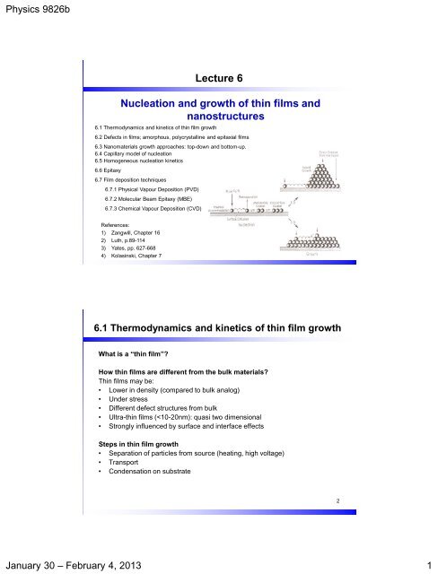
Lecture 6 Nucleation and growth of thin films and nanostructures
Lecture 6 Nucleation and growth of thin films and nanostructures
Lecture 6 Nucleation and growth of thin films and nanostructures

You also want an ePaper? Increase the reach of your titles
YUMPU automatically turns print PDFs into web optimized ePapers that Google loves.
Physics 9826b<br />
<strong>Lecture</strong> 6<br />
<strong>Nucleation</strong> <strong>and</strong> <strong>growth</strong> <strong>of</strong> <strong>thin</strong> <strong>films</strong> <strong>and</strong><br />
<strong>nanostructures</strong><br />
6.1 Thermodynamics <strong>and</strong> kinetics <strong>of</strong> <strong>thin</strong> film <strong>growth</strong><br />
6.2 Defects in <strong>films</strong>; amorphous, polycrystalline <strong>and</strong> epitaxial <strong>films</strong><br />
6.3 Nanomaterials <strong>growth</strong> approaches: top-down <strong>and</strong> bottom-up.<br />
6.4 Capillary model <strong>of</strong> nucleation<br />
6.5 Homogeneous nucleation kinetics<br />
6.6 Epitaxy<br />
6.7 Film deposition techniques<br />
6.7.1 Physical Vapour Deposition (PVD)<br />
6.7.2 Molecular Beam Epitaxy (MBE)<br />
6.7.3 Chemical Vapour Deposition (CVD)<br />
References:<br />
1) Zangwill, Chapter 16<br />
2) Luth, p.89-114<br />
3) Yates, pp. 627-668<br />
4) Kolasinski, Chapter 7<br />
1<br />
6.1 Thermodynamics <strong>and</strong> kinetics <strong>of</strong> <strong>thin</strong> film <strong>growth</strong><br />
What is a “<strong>thin</strong> film”?<br />
How <strong>thin</strong> <strong>films</strong> are different from the bulk materials?<br />
Thin <strong>films</strong> may be:<br />
• Lower in density (compared to bulk analog)<br />
• Under stress<br />
• Different defect structures from bulk<br />
• Ultra-<strong>thin</strong> <strong>films</strong> (
Physics 9826b<br />
Detailed steps in film formation<br />
1. Thermal accommodation<br />
2. Binding (physisorption <strong>and</strong> chemisorption)<br />
3. Surface diffusion (typically larger than bulk diffusion)<br />
4. <strong>Nucleation</strong><br />
5. Isl<strong>and</strong> <strong>growth</strong><br />
6. Coalescence<br />
7. Continued <strong>growth</strong><br />
<strong>Nucleation</strong> <strong>and</strong> <strong>growth</strong> occurs on defects (or sites with higher bonding<br />
energy)<br />
3<br />
Three different <strong>growth</strong> modes<br />
1. Isl<strong>and</strong> <strong>growth</strong> (Volmer – Weber)<br />
3D isl<strong>and</strong>s formation; film atoms more strongly bound to each other than to<br />
substrate <strong>and</strong>/ or slow diffusion<br />
2. Layer-by-layer <strong>growth</strong> (Frank – van der Merwe)<br />
generally the highest crystalline quality; film atoms more strongly bound to<br />
substrate than to each other <strong>and</strong>/or fast diffusion<br />
3. Stranski – Krastanov (mixed <strong>growth</strong>)<br />
initially layer-by-layer, then 2D isl<strong>and</strong>s<br />
<strong>Lecture</strong> 10 4<br />
January 30 – February 4, 2013 2
Physics 9826b<br />
Thin film <strong>growth</strong> is not an equilibrium process!<br />
1. Thermodynamics (Gibbs Free energy <strong>and</strong> phase diagram): can the sold phase<br />
be formed at the given temperature?<br />
2. Kinetics (deposition rate <strong>and</strong> diffusion rate)<br />
Artificial superlattice is the best example <strong>of</strong> manipulating kinetics <strong>and</strong><br />
thermodynamics<br />
5<br />
6.2 Defects in Films<br />
Can be divided according to their geometry <strong>and</strong> shape<br />
• 0-D or point defects<br />
• 1-D or line defects (dislocations)<br />
• 2-D <strong>and</strong> 3D (grain boundaries, crystal twins, twists, stacking faults, voids<br />
<strong>and</strong> precipitates)<br />
Compression<br />
Edge<br />
dislocation<br />
line<br />
Tension<br />
6<br />
January 30 – February 4, 2013 3
Physics 9826b<br />
1D (Linear) defects<br />
• 1D or linear defect - dislocations<br />
- edge dislocation<br />
- screw dislocation<br />
• Edge dislocation (an extra partial plane <strong>of</strong> atoms)<br />
• there will be local lattice distortion (relaxed at long<br />
distance)<br />
• Strain fields (compression <strong>and</strong> tension)<br />
Compression<br />
Edge<br />
dislocation<br />
line<br />
Tension<br />
Mathematically slip or Burger vector b is<br />
used to characterize displacement <strong>of</strong> atoms<br />
around the dislocation<br />
b is perpendicular to the edge-dislocation line<br />
7<br />
1D - Screw dislocation<br />
By following a loop <strong>of</strong> atoms around dislocation line end up one<br />
plane up or down<br />
Burger vector is parallel to the screw dislocation line<br />
8<br />
January 30 – February 4, 2013 4
Physics 9826b<br />
Mixed edge <strong>and</strong> screw dislocations<br />
Most dislocations found in crystalline material are neither pure edge<br />
nor pure screw, but exhibit components <strong>of</strong> both types<br />
9<br />
3D defects<br />
Crystal twins<br />
Grain boundary is not r<strong>and</strong>om, but have a symmetry (ex.:<br />
mirror)<br />
Stacking faults<br />
fcc: …ABCABC…<br />
…ABCABABCABC…<br />
Crystal twin<br />
Stacking fault<br />
Voids the absence <strong>of</strong> a number <strong>of</strong> atoms to form internal<br />
surfaces; similar to microcracks (broken bonds at the<br />
surface)<br />
Based on crystallinity:<br />
amorphous; polycrystalline <strong>and</strong> epitaxal (single crystal)<br />
10<br />
January 30 – February 4, 2013 5
Physics 9826b<br />
6.3 Nanomaterials <strong>growth</strong> methods<br />
Two approaches<br />
Top-down<br />
Patterning in bulk materials by<br />
combination <strong>of</strong><br />
Lithography<br />
Etching<br />
Deposition<br />
- can be applied for variety <strong>of</strong> materials<br />
- limited by lithography resolution,<br />
selectivity <strong>of</strong> etching, etc.<br />
Bottom-up<br />
Structure is assembled from well-defined<br />
chemically or physically synthesized<br />
building blocks<br />
Self-assembly<br />
Selective <strong>growth</strong><br />
- require accurate control <strong>and</strong> tunable<br />
chemical composition, structure, size <strong>and</strong><br />
morphology <strong>of</strong> building blocks<br />
- in principle limited only by atomic<br />
dimensions<br />
11<br />
Mechanical Methods (Mechanosynthesis)<br />
Low cost fabrication: ball milling or shaker milling<br />
Kinetic energy from a rotating or vibrating canister is imparted to hard spherical<br />
ball bearings (under controlled atmosphere)<br />
(1) Compaction <strong>and</strong> rearrangement <strong>of</strong> particles<br />
(2) First elastic <strong>and</strong> then severe plastic deformation <strong>of</strong><br />
the sample material formation <strong>of</strong> defects <strong>and</strong><br />
dislocations<br />
(3) Particle fracture <strong>and</strong> fragmentation with continuous<br />
size reduction formation <strong>of</strong> nanograined material<br />
1 KIC<br />
E<br />
<br />
F<br />
~ ~<br />
Y a a<br />
F – stress level, when crack propagation leads to<br />
fracture; - surface energy <strong>of</strong> the particle; a - length<br />
<strong>of</strong> a crack<br />
K<br />
IC<br />
Y<br />
F<br />
a<br />
-material with defects with a wide distribution <strong>of</strong> size<br />
<strong>Lecture</strong> 10 12<br />
January 30 – February 4, 2013 6
Physics 9826b<br />
High-Energy Methods: Discharge Plasma Method<br />
Application <strong>of</strong> high energy electric current (monochromatic radiation – laser ablation)<br />
Can be used for fullerenes <strong>and</strong> C nanotubes<br />
Process depend on:<br />
-Pressure <strong>of</strong> He, process temperature,<br />
applied current<br />
final product requires extensive purification<br />
13<br />
Structure <strong>of</strong> the carbon nanotubes<br />
armchair<br />
zig-zag<br />
chiral<br />
<strong>Lecture</strong> 10 14<br />
January 30 – February 4, 2013 7
Physics 9826b<br />
Carbon Nanotubes<br />
The structure can be specified by vector (n, m)<br />
which defines how the graphene sheet is rolled up<br />
A nanotube with the indices (6,3): the sheet is<br />
rolled up so that the atom (0,0) is superimposed<br />
on the one labeled (6,3)<br />
m = 0 for all zig-zag tubes, while n = m for all<br />
armchair tubes<br />
15<br />
Chemical Fabrication Methods<br />
Anodizing (<strong>and</strong> electropolishing)<br />
Insulating porous oxide layer is created on a conductive metal anode in electrolytic solution<br />
Anodic reaction<br />
2Al 0 (s) 2 Al 3+ + 6e<br />
Oxide-electrolyte interface 2 Al 3+ + 3H 2 O 2 Al 2 O 3 + 6H +<br />
Cathodic reaction 6H + + 6e 3 H 2 (g)<br />
Overall oxide formation reaction:<br />
2Al 0 (s) + 3H 2 O Al 2 O 3 + 3 H 2<br />
Porous Al 2 O 3 membranes can be<br />
considered as ultimate template material<br />
16<br />
January 30 – February 4, 2013 8
Physics 9826b<br />
Lithographic Methods<br />
17<br />
Top-bottom: High-Aspect Aspect-Ratio Si Structures<br />
nanotextured Si surface<br />
dense silicon pillar array<br />
18<br />
January 30 – February 4, 2013 9
Physics 9826b<br />
Bottom-up: vapor-liquid-solid <strong>growth</strong><br />
• Metal particle catalyzed the decomposition <strong>of</strong> a<br />
gaseous species containing the semiconductor<br />
components, e.g. Ge, or Ga <strong>and</strong> As<br />
• Metal catalyst particles absorb species,<br />
becoming saturated with them at eutectic point<br />
(relatively low temperature)<br />
• When semiconductor reaches supersaturation,<br />
it precipitates out <strong>of</strong> the eutectic<br />
• Metal prepared <strong>and</strong> deposited/grown on surface<br />
• Metal droplet size determines eventual wire<br />
diameter<br />
VLS <strong>growth</strong> <strong>of</strong> Ge NWsw/Au<br />
(from E. Garfunkel)<br />
19<br />
Cartoon <strong>of</strong> <strong>growth</strong><br />
Metallic<br />
catalyst<br />
nanocluster<br />
Eutectic (AuGe alloy)<br />
Temperature is<br />
controlled to keep it in<br />
the liquid state<br />
Nanowire<br />
nucleation begins<br />
when the liquid<br />
become saturated<br />
with Ge<br />
Nanowire <strong>growth</strong><br />
continues as long<br />
as Au-Ge alloy stays<br />
liquid <strong>and</strong> Ge<br />
concentration is high<br />
enough<br />
20<br />
January 30 – February 4, 2013 10
Physics 9826b<br />
Designed Synthesis <strong>of</strong> Hierarchical Structures<br />
The evolution <strong>of</strong> nanowire structural <strong>and</strong> compositional complexity<br />
enabled today by controlled synthesis<br />
(a) from homogeneous materials<br />
(b) axial <strong>and</strong> radial heterostructures<br />
(c) branched heterostructures<br />
The colors indicate regions with distinct chemical composition <strong>and</strong>/or doping<br />
21<br />
Organization <strong>and</strong> Assembly <strong>of</strong> Nanowires<br />
Using a patterned catalyst, NWs can be directly grown on a solid substrate in a<br />
designed configuration<br />
NW materials produced under synthetic conditions optimized for their <strong>growth</strong><br />
can be organized into arrays by several techniques<br />
(1) electric - field – directed (highly anisotropic structures <strong>and</strong> large polarization)<br />
(2) fluidic - flow – directed (passing a suspension <strong>of</strong> NWs through micr<strong>of</strong>luidic<br />
channel structure)<br />
(3) Langmuir–Blodgett (ordered monolayer is formed on water <strong>and</strong> transferred<br />
to a substrate)<br />
(4) patterned chemical assembly or imprint<br />
22<br />
January 30 – February 4, 2013 11
Physics 9826b<br />
Imprint based patterning <strong>of</strong> metal nanoparticles<br />
23<br />
6.4 Homogeneous Capillary Model <strong>of</strong> <strong>Nucleation</strong><br />
<br />
G total<br />
3<br />
4 r<br />
<br />
4r<br />
2 <br />
3 <br />
G total – total free-energy change<br />
r<br />
<br />
<br />
– radius <strong>of</strong> embryo or nucleus<br />
– volume free energy<br />
- specific surface free energy<br />
Two components: (i) volume freeenergy<br />
change (G V or ) <strong>and</strong> (ii)<br />
surface free-energy change (G S )<br />
0;<br />
<br />
S<br />
S<br />
L<br />
(i) is negative,<br />
(ii) G S is positive<br />
L<br />
r* - critical radius<br />
-if r < r*, droplet can shrink or dissolve<br />
-if r > r*, droplet grows<br />
24<br />
January 30 – February 4, 2013 12
Physics 9826b<br />
Critical radius, r*<br />
We can find the value <strong>of</strong> the critical radius by setting:<br />
Growth cannot proceed until a droplet with<br />
radius at least as large as r* forms<br />
The energy <strong>of</strong> this critical nucleus relatively to<br />
the liquid phase is:<br />
3 2<br />
* 16<br />
v<br />
G<br />
<br />
2<br />
( )<br />
r* decreases as T C ; H C , or <br />
25<br />
6.5 Homogeneous <strong>Nucleation</strong> Kinetics<br />
(a) <strong>Nucleation</strong> in 1st layer: compact isl<strong>and</strong>s<br />
The model:<br />
- assume nucleation in layer 1 <strong>and</strong> slow adatom desorption<br />
- assume critical nucleus is 1 atom, so that a dimer, once formed, will not dissociate. New<br />
adatoms can form new nuclei by collision with another adatom, or can add to existing<br />
nuclei<br />
- calculate saturation density N <strong>of</strong> nuclei<br />
N is reached when adatom diffuses distance L to find existing nucleus before meeting<br />
another atom<br />
The diffusion time t L over distance L, diffusion coefficient D is<br />
2<br />
L<br />
t<br />
L<br />
<br />
D<br />
Rate<br />
Rate<br />
attach<br />
flux<br />
A<br />
n<br />
<br />
t<br />
A<br />
F<br />
Campbell, Surf. Sci. Rep. 27 (1997) 1-111<br />
L<br />
2D<br />
<strong>Lecture</strong> 10 26<br />
January 30 – February 4, 2013 13
Physics 9826b<br />
Homogeneous <strong>Nucleation</strong> Kinetics<br />
- At steady state, when no new nuclei are created<br />
Rate Rate<br />
flux<br />
n<br />
A<br />
F A<br />
t<br />
2D<br />
L<br />
attach<br />
n2DD<br />
A<br />
2<br />
L<br />
Solve for n 2D :<br />
- Assume two atoms for a dimer when they sit on adjacent sites separated by a<br />
D<br />
2<br />
Ratedimer<br />
A<br />
n2D<br />
khop<br />
pocc<br />
A<br />
n2D<br />
4n2Da<br />
2<br />
a<br />
2<br />
Rate 4ADn<br />
Rate<br />
4Dn<br />
dimer<br />
dimer<br />
2D<br />
<br />
4ADn<br />
1<br />
10<br />
Rate<br />
D 4<br />
L <br />
2<br />
t (10L<br />
)<br />
L<br />
2D<br />
2<br />
2D<br />
attach<br />
n2D<br />
A<br />
t<br />
D<br />
40F<br />
L<br />
- Saturation should be assured when enough nuclei have formed<br />
to have average separation L, so that saturation density is<br />
(b) Dendritic Growth in 1 st layer: - aside<br />
C. Ratsch PRL 72 (1994) 3194<br />
27<br />
6.6 Epitaxy<br />
Epitaxy (“arrangement on”) refers loosely to control <strong>of</strong> the orientation <strong>of</strong> the<br />
growing phase by the crystal structure <strong>of</strong> the substrate<br />
homoepitaxy: host <strong>and</strong> growing phase are the same material<br />
heteroepitaxy: host <strong>and</strong> growing phase are different<br />
Orientation <strong>and</strong> Strain<br />
There exist orientational relations between dissimilar crystal lattices in contact<br />
(e.g., fcc (111)/bcc (110); fcc (100) /rocksalt (100)<br />
Nishiyama-<br />
Wasserman<br />
Kurdjimov<br />
-Sachs<br />
Zangwill, Ch.16 28<br />
January 30 – February 4, 2013 14
Physics 9826b<br />
Epitaxial energy<br />
NW: Q = 0 o , row-matching parallel to [001] bcc<br />
KS: Q = 5.26 o , rotational epitaxy<br />
Definition <strong>of</strong> misfit:<br />
a b<br />
f <br />
a<br />
Epitaxial energy at interface calculated<br />
using Lennard-Jones pairwise 6-12 potential<br />
Note minima for 0 o <strong>and</strong> ~ 5 o<br />
E is indep. <strong>of</strong> r = a/b for other angles<br />
Heterointerface between 2 diff. crystals:<br />
the lattice mismatch is adjusted by<br />
edge dislocations or strain<br />
Zangwill, Ch.16 29<br />
Strained vs Dislocations<br />
The type <strong>of</strong> interface (strained vs dislocations) depends on the thickness <strong>of</strong> the film <strong>and</strong><br />
lattice mismatch, f.<br />
The energy stored in an interface between epitaxial film <strong>and</strong> substrate is calculated from<br />
the relative contributions <strong>of</strong> elastic strain (deformation <strong>of</strong> the lattice <strong>of</strong> the film) <strong>and</strong><br />
formation <strong>of</strong> edge dislocations<br />
Left: film thickness = const.<br />
Right: misfit = const.<br />
Often, pseudomorphic <strong>growth</strong> is found for the first monolayer or so in metals on<br />
metals (i.e., overlayer adopts atomic arrangements <strong>of</strong> substrate)<br />
As film thickness , complexities develop….<br />
30<br />
January 30 – February 4, 2013 15
Physics 9826b<br />
Structural phase diagram<br />
We can illustrate the complexity <strong>of</strong> <strong>growth</strong> in the case <strong>of</strong> fcc(111)/bcc(110)<br />
inteface in plot <strong>of</strong> r vs l<br />
a<br />
r <br />
b<br />
coupling strenth wi<strong>thin</strong> film<br />
l <br />
interlayer coupling strenth<br />
<strong>Lecture</strong> 10 31<br />
6.7 Film deposition techniques<br />
1. Physical Vapour Deposition (PVD)<br />
Evaporation: thermal <strong>and</strong> electron-beam assisted<br />
Sputtering: RF <strong>and</strong> DC Magnetron<br />
Pulsed Laser Deposition (PLD)<br />
3. Molecular Beam Epitaxy (MBE)<br />
2. Chemical Vapour Deposition (CVD)<br />
Plasma-Enhanced CVD (PE-CVD)<br />
Atomic Layer Deposition (ALD)<br />
Need good vacuum for <strong>thin</strong> film <strong>growth</strong>!<br />
32<br />
January 30 – February 4, 2013 16
Physics 9826b<br />
6.7.1 Physical Vapour Deposition (PVD)<br />
Thermal Evaporation for non-refractory materials<br />
E-beam evaporation for refractory materials<br />
http://www.mdc-vacuum.com<br />
<strong>Lecture</strong> 10 33<br />
Leybold Product <strong>and</strong> Vacuum Technology Reference <strong>Lecture</strong> 10 Book<br />
34<br />
January 30 – February 4, 2013 17
Physics 9826b<br />
Sputtering Deposition<br />
• DC for conducting materials<br />
• RF for insulating materials<br />
Magnetron sputtering is most popular due to high rate <strong>and</strong> low operation<br />
pressure<br />
<strong>Lecture</strong> 10 35<br />
Pulsed Laser Deposition (PLD)<br />
• Good for multielemental materials (P < 1 Torr)<br />
<strong>Lecture</strong> 10 36<br />
January 30 – February 4, 2013 18
Physics 9826b<br />
6.7.2 Molecular Beam Epitaxy (MBE)<br />
Molecular Beam Epitaxy<br />
(p < 10 -8 Torr)<br />
1. Elemental Superlattices: Giant<br />
Magneto-Resistiance (GMR)<br />
Devices<br />
2. Binary III-V Superlattices<br />
3. Complex Oxide Superlattices<br />
37<br />
Complex oxides are not that complex:<br />
Most <strong>of</strong> them are based on the ABO3 cubic perovskite structure<br />
Ex.:: SrTiO3, LaTiO3, LaMnO3, LaAlO3, …<br />
Favorable to atomically smooth layered heterostructures<br />
ABO3<br />
A: M2+ (Ca, Sr, Ba, La)<br />
B: M4+ (Ti, Zr, Mn)<br />
38<br />
January 30 – February 4, 2013 19
Physics 9826b<br />
Superlattices grown by MBE<br />
LaTiO 3 /SrTiO 3 (PLD)<br />
M. Warusawithana, J. Zuo, H. Chen<br />
<strong>and</strong> J. N. Eckstein<br />
A. Ohtomo, H. Y. Hwang, Nature 419, 378<br />
(2002)<br />
39<br />
6.7.3 Chemical Vapour Deposition (CVD)<br />
SrTiO 3 /BaTiO 3 /CaTiO 3<br />
<strong>Lecture</strong> 10 40<br />
Precursors are needed!<br />
CH 4 (g) SWNT + H 2 (g) ~ 700 o C, Fe, Ni catalysts<br />
SiH 4 (g) Si + 2 H 2 (g)<br />
Si(OC 2 H 5 ) 4 (g) SiO 2 (s) + (C 2 H 5 ) 2 O (g)<br />
January 30 – February 4, 2013 20
Physics 9826b<br />
Atomic Layer Deposition<br />
H 2 O<br />
HCl<br />
1. MCl 4 exposure<br />
2. Purge<br />
3. H 2 O exposure<br />
4. Purge MO 2 ML<br />
Si<br />
MCl 4 (ads, surf) + 2 H 2 O(g) MO 2 (s) + 4HCl(g)<br />
M(N(CH 3 )(C 2 H 5 )) 4 (ads, surf) + O 3 (g) MO 2 (s) + …<br />
• Surface saturation controlled process<br />
•Excellent film quality <strong>and</strong> step coverage<br />
41<br />
January 30 – February 4, 2013 21