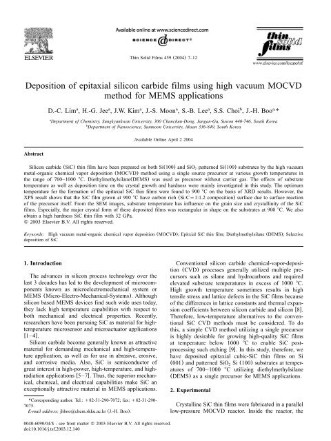
Deposition of epitaxial silicon carbide films using high vacuum ...
Deposition of epitaxial silicon carbide films using high vacuum ...
Deposition of epitaxial silicon carbide films using high vacuum ...

Create successful ePaper yourself
Turn your PDF publications into a flip-book with our unique Google optimized e-Paper software.
Thin Solid Films 459 (2004) 7–12<br />
<strong>Deposition</strong> <strong>of</strong> <strong>epitaxial</strong> <strong>silicon</strong> <strong>carbide</strong> <strong>films</strong> <strong>using</strong> <strong>high</strong> <strong>vacuum</strong> MOCVD<br />
method for MEMS applications<br />
a a a a a b a,<br />
D.-C. Lim , H.-G. Jee , J.W. Kim , J.-S. Moon , S.-B. Lee , S.S. Choi , J.-H. Boo *<br />
a<br />
Department <strong>of</strong> Chemistry, Sungkyunkwan University, 300 Chunchun-Dong, Jangan-Gu, Suwon 440-746, South Korea<br />
b<br />
Department <strong>of</strong> Nanoscience, Sunmoon University, Ahsan 336-840, South Korea<br />
Available Online April 2 2004<br />
Abstract<br />
Silicon <strong>carbide</strong> (SiC) thin film have been prepared on both Si(100) and SiO patterned Si(100) substrates by the <strong>high</strong> <strong>vacuum</strong><br />
2<br />
metal-organic chemical vapor deposition (MOCVD) method <strong>using</strong> a single source precursor at various growth temperatures in<br />
the range <strong>of</strong> 700–1000 8C. Diethylmethylsilane(DEMS) was used as precursor without carrier gas. The effects <strong>of</strong> substrate<br />
temperature as well as deposition time on the crystal growth and hardness were mainly investigated in this study. The optimum<br />
temperature for the formation <strong>of</strong> the <strong>epitaxial</strong> SiC thin <strong>films</strong> were found to 900 8C on the basis <strong>of</strong> XRD results. However, the<br />
XPS result shows that the SiC film grown at 900 8C have carbon rich (Si:Cs1:1.2 composition) surface due to surface reaction<br />
<strong>of</strong> the precursor itself. From the SEM images, substrate temperature has influence on the grain size and crystallinity <strong>of</strong> the SiC<br />
<strong>films</strong>. Especially, the major crystal form <strong>of</strong> these deposited <strong>films</strong> was rectangular in shape on the substrates at 900 8C. We also<br />
obtain a <strong>high</strong> hardness SiC thin film with 32 GPa.<br />
2003 Elsevier B.V. All rights reserved.<br />
Keywords: High <strong>vacuum</strong> metal-organic chemical vapor deposition (MOCVD); Epitxial SiC thin film; Diethylmethylsilane (DEMS); Selective<br />
deposition <strong>of</strong> SiC<br />
1. Introduction<br />
The advances in <strong>silicon</strong> process technology over the<br />
last 3 decades has led to the development <strong>of</strong> microcomponents<br />
known as microelectromechanical system or<br />
MEMS (Micro-Electro-Mechanical-Systems). Although<br />
<strong>silicon</strong> based MEMS devices find such wide uses today,<br />
they lack <strong>high</strong> temperature capabilities with respect to<br />
both mechanical and electrical properties. Recently,<br />
researchers have been pursuing SiC as material for <strong>high</strong>temperature<br />
microsensor and microactuator applications<br />
w1–4x.<br />
Silicon <strong>carbide</strong> become generally known as attractive<br />
material for demanding mechanical and <strong>high</strong>-temperature<br />
application, as well as for use in abrasive, erosive,<br />
and corrosive media. Also, SiC is semiconductor <strong>of</strong><br />
great interest in <strong>high</strong>-power, <strong>high</strong>-temperature, and <strong>high</strong>radiation<br />
applications w5–7x. Thus, the superior mechanical,<br />
chemical, and electrical capabilities make SiC an<br />
exceptionally attractive material in MEMS applications.<br />
*Corresponding author. Tel.: q82-31-290-7072; fax: q82-31-290-<br />
7075.<br />
E-mail address: jhboo@chem.skku.ac.kr (J.-H. Boo).<br />
Conventional <strong>silicon</strong> <strong>carbide</strong> chemical-vapor-deposition<br />
(CVD) processes generally utilized multiple precursors<br />
such as silane and hydrocarbons and required<br />
elevated substrate temperatures in excess <strong>of</strong> 1000 8C.<br />
High growth temperature sometimes results in <strong>high</strong><br />
tensile stress and lattice defects in the SiC <strong>films</strong> because<br />
<strong>of</strong> the differences in lattice constants and thermal expansion<br />
coefficients between <strong>silicon</strong> <strong>carbide</strong> and <strong>silicon</strong> w8x.<br />
Therefore, low-temperature alternatives to the conventional<br />
SiC CVD methods must be considered. To do<br />
this, a simple CVD method utilizing a single precursor<br />
is <strong>high</strong>ly desirable for growing <strong>high</strong>-quality SiC <strong>films</strong><br />
at temperature below 1000 8C to enable SiC postprocessing<br />
such etching w9x. In this study, therefore, we<br />
have deposited <strong>epitaxial</strong> cubic-SiC thin <strong>films</strong> on Si<br />
(001) and patterned SiO2<br />
Si (100) substrates at temperatures<br />
<strong>of</strong> 700–1000 8C utilizing diethylmethylsilane<br />
(DEMS) as a single precursor for MEMS applications.<br />
2. Experimental<br />
Crystalline SiC thin <strong>films</strong> were fabricated in a parallel<br />
low-pressure MOCVD reactor. Inside the reactor, the<br />
0040-6090/04/$ - see front matter 2003 Elsevier B.V. All rights reserved.<br />
doi:10.1016/j.tsf.2003.12.140
8 D.-C. Lim et al. / Thin Solid Films 459 (2004) 7–12<br />
Fig. 1. X-Ray diffraction patterns <strong>of</strong> SiC thin <strong>films</strong> grown on Si(100) substrates <strong>using</strong> DEMD at various deposition temperatures and times given<br />
in the figure.<br />
substrate was mounted on a stainless holder that was<br />
heated by DC power supply. The general CVD condition<br />
y7<br />
y5<br />
was pressures between 2.0=10 Torr and 1.0=10<br />
Torr and growth temperatures <strong>of</strong> 700–1000 8C, respectively.<br />
The substrate temperature was measured with an<br />
optical pyrometer. The deposition time was lasted to be<br />
maximum 6 h and SiC <strong>films</strong> have been grown on both<br />
Si (100) and SiO patterned Si (100) substrates.<br />
2<br />
The diethylmethylsilane (DEMS), (CH CH ) 3 2 2<br />
–SiH–CH , used in this study as single precursor, is a<br />
3<br />
liquid at room temperature with boiling point <strong>of</strong> 78 8C.<br />
This makes the handling aspects much more simplified<br />
compared with conventional dual-source CVD. Also,<br />
the use <strong>of</strong> single precursor insures stoichiometry, hence,<br />
it eliminates the need for an elaborate gas handling<br />
system.<br />
After deposition, a number <strong>of</strong> analysis and characterization<br />
techniques were employed to investigate the<br />
deposited SiC <strong>films</strong>. These include X-ray Photoemission<br />
Spectroscopy (XPS) to confirm chemical composition,<br />
X-ray diffraction (XRD) to determine structural crystallinity,<br />
and Atomic Force Microscope (AFM) to investigate<br />
SiC film topology. Scanning electron microscopy<br />
(SEM) was also used to investigate the SiC film<br />
morphology and the quality <strong>of</strong> the SiCySi interface as<br />
well as to estimate film thickness by cross-sectional<br />
image.<br />
3. Results and discussions<br />
Fig. 1 shows the X-ray u–2u diffraction patterns <strong>of</strong><br />
cubic SiC thin <strong>films</strong> grown on Si (100) surface at<br />
temperatures in the range 700–1000 8C and 1.0=10 y5<br />
Torr for different deposition time. Fig. 1a shows the<br />
XRD pattern <strong>of</strong> SiC thin film grown at 700 8C and 2 h.<br />
From Fig. 1a b, we can see that SiC thin film (1a)<br />
grown at 700 8C and 2 h has an amorphous structure.<br />
However, with increasing the deposition time to 4 h at<br />
the same temperature, the diffraction pattern shown in<br />
the Fig. 1b shows a crystal structure with (200) 3C–<br />
SiC plane (2us41.48) as well as the graphite carbon<br />
structure (2us45.28). This indicates that with single<br />
precursor MOCVD crystalline 3C–SiC film can be<br />
deposited at much lower temperature than conventional<br />
CVD. With increasing the deposition temperatures from<br />
700 to 900 8C, moreover, a significant increase <strong>of</strong> the<br />
intensity <strong>of</strong> 3C–SiC (002) diffraction peaks was<br />
observed, showing an improvement <strong>of</strong> crystallinity. The<br />
XRD pattern (see Fig. 2c) <strong>of</strong> 3C–SiC thin film grown<br />
at 900 8C exhibits a very large and sharp peak at the<br />
(200) reflection <strong>of</strong> 2us41.48. This indicates that this<br />
thin film was grown <strong>epitaxial</strong>ly and may have a monocrystalline<br />
nature with (200) preferred orientation. However,<br />
in the Fig. 1d, small peaks attributed to the 3C–<br />
SiC(111) diffraction also appeared in addition to major
D.-C. Lim et al. / Thin Solid Films 459 (2004) 7–12<br />
9<br />
Fig. 2. SEM images <strong>of</strong> SiC thin <strong>films</strong> grown on Si(100) substrates <strong>using</strong> DEMS at various deposition temperatures.<br />
peaks <strong>of</strong> 3C–SiC (200) diffraction, indicating that<br />
polycrystalline 3C–SiC thin film was obtained at deposition<br />
temperatures <strong>of</strong> 1000 8C. From our XRD data,<br />
with increasing the deposition temperature from 700 to<br />
900 8C, <strong>high</strong> quality 3C–SiC layer was obtained under<br />
the same deposition conditions. The XRD results also<br />
show that the deposition time as well as deposition<br />
temperature could be one <strong>of</strong> the important factors for<br />
influencing the film crystallinity.<br />
Fig. 2 shows surface morphology changes <strong>of</strong> the 3C–<br />
SiC <strong>films</strong> grown at various temperatures (700–1000 8C)<br />
for 2 h under the same deposition pressure <strong>of</strong> 1.0<br />
y5<br />
Torr=10 Torr, respectively. We can see that the film<br />
grown at 700 8C has a smooth surface and nano size<br />
SiC crystals as shown in the Fig. 2a. With increasing<br />
the deposition temperature, 3C–SiC film with relatively<br />
large crystals were deposited. The surface morphologies<br />
<strong>of</strong> the <strong>films</strong> grown at 900 and 1000 8C show much<br />
larger crystal size than those <strong>of</strong> the <strong>films</strong> grown at 700<br />
and 800 8C. The SEM image <strong>of</strong> SiC film grown at 800<br />
8C shown in the Fig. 2b exhibits a crystal shape <strong>of</strong> SiC<br />
crystals with sub-micron size. Above 800 8C, the crystal<br />
size and crystallinity <strong>of</strong> the 3C–SiC <strong>films</strong> are apparently<br />
limited to the substrate temperature. Especially, from the<br />
Fig. 2c, we can see that the major crystal form <strong>of</strong> a<br />
deposited film grown on the substrate at 900 8C is<br />
rectangular in shape. We also confirm the crystal form<br />
<strong>of</strong> the SiC film deposited at 900 8C from a AFM result<br />
(see Fig. 4a,c). However, a polycrystalline shape with<br />
relatively larger crystal size can be seen in Fig. 2d,<br />
when the growth temperature was at 1000 8C. This is<br />
in good agreement with the XRD result shown in the<br />
Fig. 1d.<br />
Film stoichiometry <strong>of</strong> the 3C–SiC film with optimized<br />
expitaxial crystal structure was determined utilizing<br />
the XPS analysis. The survey spectrum <strong>of</strong> Fig. 3a<br />
clearly shows the photoelectron peaks <strong>of</strong> Si 2s, Si 2p,<br />
C1s and C (KLL) Auger signals indicating formation<br />
<strong>of</strong> <strong>silicon</strong> <strong>carbide</strong> film. Oxygen (O 1s) can be attributed<br />
to surface contamination by moisture during sample<br />
transfer in the air condition. Also, we could see that the<br />
carbon content decreased after the Ar ion sputtering as<br />
shown in the Fig. 3c. As the sputtering depth is less<br />
than 3 nm, the carbon is the adsorbed species on the<br />
SiC surface. The reason for arising the carbon content<br />
on the surface is mainly due to the air contamination<br />
after deposition. In Fig. 3b, the Si 1s <strong>high</strong>-resolution<br />
spectra obtained before and after Ar ion sputtering are<br />
also shown. To compare the change <strong>of</strong> Si 1s binding<br />
energies for the SiC film before and after Ar ion<br />
sputtering, the Si 1s peak at 100.9 eV obtained without<br />
Ar ion sputtering is shifted to lower binging energy at<br />
100.3 eV after Ar ion sputtering. The reason for this<br />
binding energy shift is due to increasing <strong>of</strong> carbidic<br />
after removing <strong>of</strong> graphite carbon and surface SiO x<br />
species by Ar ion sputtering. However, we also see<br />
weak carbon shoulder peak in Fig. 5c but if we did<br />
more Ar ion sputtering the graphite carbon can be
10 D.-C. Lim et al. / Thin Solid Films 459 (2004) 7–12<br />
Fig. 3. X-Ray photoelectron spectra <strong>of</strong> a 3C–SiC thin film grown on Si (100) substrate at 900 8C obtained before and after Ar ion sputtering;<br />
(a) Survey spectrum, (b) High-resolution XP spectra <strong>of</strong> Si 2p and (c) High-resolution XP spectra <strong>of</strong> C 1s.<br />
removed completely. The stoichiometry <strong>of</strong> this film is<br />
Si: Cs1: 1.2.<br />
Fig. 4a,c show the atomic force microscopic (AFM)<br />
images <strong>of</strong> 3C–SiC thin <strong>films</strong> grown on both the Si(100)<br />
substrate (Fig. 4a) and SiO2<br />
patterned Si(100) substrate<br />
(Fig. 4c) at 900 8C. We can see the crystal size, the<br />
crystal shape and surface roughness <strong>of</strong> the 3C–SiC thin<br />
film clearly. The crystal size <strong>of</strong> the 3C–SiC is approximately<br />
0.1 mm and RMS roughness value is ;32 nm<br />
in the Fig. 4a. The 3C–SiC thin film also has rectangular<br />
crystal shape. In the Fig. 4c, however, the 3C–SiC thin<br />
film grown on SiO2<br />
patterned Si(100) substrate has<br />
more small crystal size and smooth surface with RMS<br />
roughness value approximately 6 nm than that <strong>of</strong> the<br />
3C–SiC thin film grown on Si(100) substrate. The<br />
reason for this result can be explained by the fact that<br />
a very thin SiO layer remained on the Si(100) substrate<br />
2<br />
since the substrate was transferred from air to <strong>vacuum</strong><br />
condition after the wet etching process. That’s why the<br />
SiC film was grown in a different way compared with<br />
clean Si(100) substrate. Fig. 4b shows the cross-sectional<br />
TEM image and plane view TED pattern obtained<br />
<strong>using</strong> the same film as Fig. 4a. The contrast seen in the<br />
cross-sectional view TEM micrographs is believed to be<br />
associated with mass contrast due to surface roughness<br />
andyor misoriented or twinned regions surrounding the<br />
<strong>epitaxial</strong> growth w10x. The thickness <strong>of</strong> the SiC film is<br />
approximately 150 nm. Also, the SiC film has very<br />
sharp interface and <strong>high</strong> dense crystal structure. In the<br />
TED, besides the normal diffraction pattern due to the<br />
cubic structure, extra pattern can be seen indicating the<br />
existence <strong>of</strong> microtwins and stacking faults caused by<br />
the lattice dismatch between the SiC film and the Si<br />
(100) substrate.<br />
Fig. 5a shows the optical microscopic image <strong>of</strong> a<br />
3C–SiC thin film grown on a SiO2<br />
patterned Si (100)<br />
surface at 900 8C. With conventional <strong>high</strong>-temperature<br />
CVD method, SiC <strong>films</strong> deposited on SiO2<br />
patterned<br />
Si(100) substrate have larger grain size and rougher<br />
texture and become subsequently more porous than <strong>films</strong><br />
grown on Si(100). As a result, the SiC <strong>films</strong> on SiO 2<br />
mask is more readily etched away in concentrated HF<br />
solution w11–13x while the SiC film on the Si(100) side<br />
is not clearly etched and etching takes a long time.<br />
Therefore we have selectively deposited the 3C–SiC<br />
thin film on SiO patterned Si (100) surface which<br />
2
D.-C. Lim et al. / Thin Solid Films 459 (2004) 7–12<br />
11<br />
surface. To confirm this selectivity characteristic on<br />
SiO2<br />
patterned Si(100) substrate, we measure the EDX<br />
(see Fig. 5c,d). Si and C species were detected in the<br />
zone a while Si and O species were only detected in<br />
zone b. Carbon species contributed to SiC was not<br />
detected in zone b. From these results, we could derive<br />
that the SiC film was deposited selectively on the SiO 2<br />
patterned Si(100) substrate. Therefore, we could etch<br />
away the SiO layer more easily and get the deposited<br />
2<br />
SiC film only by lifting <strong>of</strong>f the SiO from the Si(100)<br />
2<br />
substrate, suggesting good MEMS applications. Fig. 5b<br />
shows the SEM images <strong>of</strong> SiC thin film after SiO 2<br />
pattern etched away <strong>using</strong> HF solution. Also, we measured<br />
the hardness <strong>of</strong> SiC thin <strong>films</strong> <strong>using</strong> the micro<br />
knoop hardness tester. Independently the deposition<br />
temperature, the SiC thin <strong>films</strong> grown under the same<br />
deposition conditions have <strong>high</strong> hardness approximately<br />
32 GPa.<br />
4. Conclusions<br />
Fig. 4. AFM images SiC thin <strong>films</strong> grown on both Si(100) (a) and<br />
SiO2<br />
patterned Si(100) (b) substrates <strong>using</strong> DEMS at 900 8C. Fig.<br />
4b shows TEM images <strong>of</strong> the same SiC thin film as Fig. 4a. The<br />
insert <strong>of</strong> Fig. 4a shows TED pattern <strong>of</strong> the same film.<br />
made by UV-dry etching <strong>of</strong> a mask shielded SiO layers 2<br />
after a PR coating <strong>of</strong> the oxidized Si(100) substrate. In<br />
Fig. 5a, we could clearly see the selective deposited SiC<br />
film with more rough surface than that <strong>of</strong> the SiO 2<br />
We have deposited the 3C–SiC thin <strong>films</strong> with <strong>high</strong><br />
hardness <strong>of</strong> 32 GPa on Si(100) surfaces by a diethylmethylsilane<br />
(DEMS) single precursor at temperatures<br />
y5<br />
in the range 700–1000 8C and 1.0=10 Torr for<br />
MEMS applications. With increasing the deposition<br />
temperature to 900 8C, relatively well oriented 3C–SiC<br />
layers were obtained. At this deposition condition, the<br />
major crystal form <strong>of</strong> 3C–SiC thin film was rectangular<br />
in shape on the substrate, and the average crystal size<br />
and the value <strong>of</strong> RMS surface roughness are approximately<br />
0.1 mm and ;32 nm, respectively. Otherwise,<br />
the 3C–SiC thin film grown on SiO2<br />
patterned Si(100)<br />
substrate has more small crystal size and smooth surface<br />
with RMS roughness value approximately 6 nm. With<br />
increasing deposition time from 2 h to 4 h, the crystal<br />
size as well as RMS roughness value also increased.<br />
These results show that the deposition temperature and<br />
time could be one <strong>of</strong> the important factors for influencing<br />
the film crystallinity. The XPS result shows that the<br />
SiC film grown at 900 8C has a slightly carbon rich.<br />
We have also selectively deposited cubic <strong>silicon</strong> <strong>carbide</strong><br />
thin <strong>films</strong> on SiO2<br />
patterned Si(100) substrates. In<br />
conclusion, the low-temperature chemical vapor deposition<br />
process <strong>using</strong> a single precursor for both eptixial<br />
SiC growth on Si(100) and selective SiC deposition on<br />
SiO patterned Si(100) substrates described in this study<br />
2<br />
will be readily adaptable to current MEMS applications.<br />
Acknowledgments<br />
Support <strong>of</strong> this research by the Ministry <strong>of</strong> Science<br />
Technology in Korea (project No. M10214000278-<br />
02B1500-04211) is gratefully acknowledged.
12 D.-C. Lim et al. / Thin Solid Films 459 (2004) 7–12<br />
Fig. 5. Optical microscopic (a) and SEM (b) images before and after chemical etching <strong>of</strong> SiC thin <strong>films</strong> grown on SiO2<br />
patterned Si(100)<br />
substrate <strong>using</strong> DEMS at 900 8C. Fig. 5c,d show the EDX spectra <strong>of</strong> selectively deposited SiC thin film (zone a) on SiO2<br />
patterned Si(100)<br />
substrate (zone b) obtained from the same film as Fig. 5a.<br />
References<br />
w1x S. Sundararajan, Bharat Bhushan, Wear 217 (1998) 252.<br />
w2x L. Tong, M. Mehregany, L.G. Matus, Appl. Phys. Lett. 60<br />
(1992) 2992.<br />
w3x O. Kordina, L.O. Bjorketun, A. Henry, C. Hallin, R.C. Glass,<br />
L. Hulyman, J.-E. Sundgren, E. Janzen, J. Cryst. Growth 154<br />
(1995) 303.<br />
w4x R.F. Davis, J.W. Palmour, J.A. Edmond, IEDM (1990) 785.<br />
w5x J.B. Casady, R.W. Johnson, Solid-State Electron. 39 (1996)<br />
1409.<br />
w6x E. Janzen, O. Kordina, Mater. Sci. Eng. B46 (1997) 203.<br />
w7x J.-H. Boo, S.A. Ustin, H. Wilson, Thin Solid Films 343–344<br />
(1999) 650.<br />
w8x Z. Li, R.C. Bardt, J. Am. Ceram. Soc. 70 (1987) 445.<br />
w9x C.R. Stoldt, M.C. Fritz, C. Carraro, R. Maboudian, Appl. Phys.<br />
Lett. 79 (2001) 347.<br />
w10x I. Golecki, F. Reidinger, J. Marti, Appl. Phys. Lett. 60 (1992)<br />
1703.<br />
w11x J.H. Edgar, Y. Gao, J. Chaudhuri, S. Cheema, S.A. Casalnuovo,<br />
P.W. Yip, M.V. Sidorov, J. Appl. Phys. 84 (1998) 201.<br />
w12x C.R. Stoldt, C. Carraro, W. RobertAshurst, Di. Gao, R.T.<br />
Howe, R. Maboudian, Sensor. Actuat. A 97–98 (2002) 410.<br />
w13x C.H. Wu, C.A. Zorman, M. Mehregany, Thin Solid Films 355–<br />
356 (1999) 179.