HY3118/HY3116 Datasheet
HY3118/HY3116 Datasheet
HY3118/HY3116 Datasheet

Create successful ePaper yourself
Turn your PDF publications into a flip-book with our unique Google optimized e-Paper software.
<strong>HY3118</strong>/<strong>HY3116</strong><br />
<strong>Datasheet</strong><br />
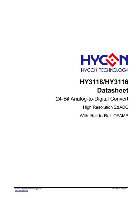
24-Bit . Analog-to-Digital Convert<br />
High Resolution Σ∆ADC<br />
With Rail-to-Rail OPAMP<br />
© 2011-2013 HYCON Technology Corp.<br />
www.hycontek.com<br />
DS-<strong>HY3118</strong>-V08_EN
<strong>HY3118</strong>/<strong>HY3116</strong><br />
24-Bit Analog-to-Digital Convert<br />
High Resolution Σ∆ADC<br />
TABLE OF CONTENTS<br />
1. FEATURES ..................................................................................................................5<br />
2. PRODUCT OVERVIEW ...............................................................................................7<br />
3. PIN DEFINITION ..........................................................................................................8<br />
3.1. Pin Diagram ........................................................................................................................................ 8<br />
3.2. I/O Pin Definition ................................................................................................................................. 8<br />
4. APPLICATION CIRCUIT..............................................................................................9<br />
4.1. Bridge Sensor ..................................................................................................................................... 9<br />
5. REGISTER LIST ........................................................................................................10<br />
.<br />
5.1. Register List ...................................................................................................................................... 10<br />
5.2. Register Description.......................................................................................................................... 11<br />
6. ELECTRICAL CHARACTERISTICS..........................................................................15<br />
6.1. Absolute Maximum Ratings .............................................................................................................. 15<br />
6.2. Electrical Characteristics................................................................................................................... 15<br />
6.3. OPAMP, Electrical Specification........................................................................................................ 20<br />
7. ENOB AND NOISE-FREE..........................................................................................21<br />
8. I 2 C COMMUNICATION PROTOCOL .........................................................................23<br />
8.1. I2C Communication Sequence Diagram ..........................................................................................23<br />
9. OVERVIEW ................................................................................................................30<br />
9.1. Frequency vs. Low Power mode ...................................................................................................... 30<br />
9.2. VDDA Power (Low Dropout Regulator) ............................................................................................32<br />
© 2011-2014 HYCON Technology Corp<br />
www.hycontek.com<br />
DS-<strong>HY3118</strong>- V08_EN<br />
Page 2
<strong>HY3118</strong>/<strong>HY3116</strong><br />
24-Bit Analog-to-Digital Convert<br />
High Resolution Σ∆ADC<br />
9.3. REFO Reference Voltage ................................................................................................................. 32<br />
9.4. Input Channel Multiplexer with IRQ .................................................................................................. 34<br />
9.5. Reference Voltage and its Input Channel with VREF .......................................................................35<br />
9.6. Measurement Signal Input Channel with PGA .................................................................................37<br />
9.7. COMB Filter ...................................................................................................................................... 40<br />
9.8. Data Conversion Format................................................................................................................... 42<br />
9.9. Rail-to-Rail OPAMP .......................................................................................................................... 43<br />
10. ORDERING INFORMATION ......................................................................................44<br />
11. PACKAGE INFORMATION........................................................................................45<br />
11.1. SSOP16 ............................................................................................................................................ 45<br />
11.2. MSOP10 ........................................................................................................................................... 46<br />
.<br />
12. REVISION RECORD..................................................................................................47<br />
© 2011-2014 HYCON Technology Corp<br />
www.hycontek.com<br />
DS-<strong>HY3118</strong>- V08_EN<br />
Page 3
<strong>HY3118</strong>/<strong>HY3116</strong><br />
24-Bit Analog-to-Digital Convert<br />
High Resolution Σ∆ADC<br />
Notes:<br />
1. Improvements and contents to this user guide necessitated by improvements to equipment may be<br />
made by Hycon Technology at any time and without notice. You may download the most up to date<br />
version of this user guide at http://www.hycontek.com.<br />
2. Under no circumstances will Hycon Technology be liable in any way for third party copyright problems<br />
concerning graphs and application circuits contained in this user guide.<br />
3. Hycon Technology guarantees that features, typical applications and functions of this product are<br />
compliant with this user guide when being used in stand-alone situation. Hycon Technology does not<br />
make the same guarantee when this product is used together with your finished goods or equipment.<br />
Hycon Technology advises you to conduct comprehensive evaluations and tests.<br />
4. You, and not Hycon Technology, are responsible for making sure that the internal power consumption<br />
of IC is within limits given in this user guide by following the using conditions of input voltage, output<br />
voltage, and load current. Under no circumstances will Hycon Technology be liable in any way for<br />
damage caused by your using this product, even for a very short period of time, in conditions<br />
exceeding limits specified in this user guide.<br />
5. In spite of embedded static protection circuit of this product Hycon Technology advises you do not<br />
apply static that is over protection circuit capacity.<br />
.<br />
6. Hycon Technology advises you not to use this product in mission critical circuits or components of<br />
mission critical circuits unless authorized with prior written permission. This may include, but not<br />
limited to, health and medical equipment, disaster prevention equipment, vehicles, automotive<br />
equipment, aviation equipment, and equipment and devices that may affect human body.<br />
7. Hycon Technology strives to improve quality and reliability of this product. However every<br />
semiconductor will fail at certain probability and this may cause personal injury and/or fire. Hycon<br />
Technology advises you to pay special attention to redundancy and safety level in designing your end<br />
product. This may prevent incidents and accidents from happening.<br />
8. Transfer and reproduction of part or all of the contents in this user guide in any format without the<br />
prior permission of Hycon Technology is prohibited.<br />
© 2011-2014 HYCON Technology Corp<br />
www.hycontek.com<br />
DS-<strong>HY3118</strong>- V08_EN<br />
Page 4
<strong>HY3118</strong>/<strong>HY3116</strong><br />
24-Bit Analog-to-Digital Convert<br />
High Resolution Σ∆ADC<br />
1. Features<br />
• Sensor’s pre-signal processing design<br />
Equipped with 24-bitΣ∆ADC analog to<br />
digital converter<br />
Embedded Rail-to-rail OPAMP<br />
Internal VDDA with sensor drive power<br />
output of up to 10mA<br />
Switchable external crystal oscillator input<br />
and high precision internal RC oscillator<br />
operating clock<br />
I2C digital transmission interface<br />
• Operation environment<br />
Digital voltage: 2.2V to 3.6V<br />
Analog voltage: 2.4V to 3.6V<br />
Operation current:<br />
1. Full speed: 1050uA (excluding OPAMP)<br />
2. Ultra-low sleep current: 1uA<br />
Operation temperature range: –40°C to<br />
+85°C<br />
• Function block diagram<br />
• 24-bits Σ∆ADC<br />
Embedded programmable preamplifier<br />
(PGA) with optional gains of: ×1, ×2, ×4,<br />
×8, ×16, ×32, ×64, and ×128.<br />
Optional data conversion output rate with<br />
upper limit of 7680Sps. 50/60Hz signal<br />
rejection at 10SPS data conversion output<br />
rate.<br />
.<br />
Embedded DC bias voltage design that can<br />
produce bias voltage at VREF multiples of 0,<br />
±1/8, ±1/4, ±3/8, ±1/2, ±5/8, ±3/4, and ±7/8<br />
RMS Noise:<br />
1. 100nV (Gain = 128) at 10 SPS output rate<br />
2. 37uV (Gain = 1) at 7680 SPS output rate<br />
3. 16 bit Noise-free resolution (Gain = 128<br />
and VREF = 3.3V)<br />
Optional input buffer for reference voltage<br />
input<br />
IRQ function<br />
• Rail-to-Rail OPAMP (<strong>HY3118</strong> only)<br />
Rail-to-rail signal input design<br />
I/O current at 1mA<br />
• Internal linear regulator VDDA and<br />
reference voltage REFO<br />
Available VDDA output voltage: 2.4V, 2.7V,<br />
3.0V or 3.3V<br />
Available REFO output voltage: 1.2V or 1.5V<br />
• I2C transmission interface:<br />
Both standard and non-standard<br />
communication format<br />
F SCL = 400KHz<br />
ADC IRQ function at non-standard mode<br />
Sleep/Wake function (for register control)<br />
• Application<br />
Weight Scale<br />
Strain Gauge<br />
Pressure Scale<br />
Industrial Process Control<br />
• Package<br />
SSOP16<br />
MSOP10<br />
© 2011-2014 HYCON Technology Corp<br />
www.hycontek.com<br />
DS-<strong>HY3118</strong>- V08_EN<br />
Page 5
<strong>HY3118</strong>/<strong>HY3116</strong><br />
24-Bit Analog-to-Digital Convert<br />
High Resolution Σ∆ADC<br />
Model No. Architecture<br />
Input<br />
Channels<br />
ENOB<br />
(Bits)<br />
<strong>HY3116</strong> Sigma-Delta 2 20<br />
<strong>HY3118</strong> Sigma-Delta 4 20<br />
RMS<br />
Noise<br />
100nV<br />
(10SPS)<br />
100nV<br />
(10SPS)<br />
System<br />
Clock<br />
Sample<br />
Rate(Max)<br />
Rail-to-Rail<br />
OPAMP<br />
DC Offset Set Interface Package<br />
Int. 327kHz/1Mhz 7680SPS NO 4 bits IIC MSOP10<br />
Int. 327kHz/1Mhz<br />
Ext.4.9152MHz<br />
7680SPS YES 4 bits IIC SSOP 16<br />
.<br />
© 2011-2014 HYCON Technology Corp<br />
www.hycontek.com<br />
DS-<strong>HY3118</strong>- V08_EN<br />
Page 6
<strong>HY3118</strong>/<strong>HY3116</strong><br />
24-Bit Analog-to-Digital Convert<br />
High Resolution Σ∆ADC<br />
2. Product Overview<br />
<strong>HY3118</strong>/<strong>HY3116</strong> is a high-precision, low-noise and low power 24-bit Analog-to-Digital<br />
converter (ADC) with embedded ultra-low-noise programmable preamplifier (PGA)<br />
featuring an effective number of bits at 21bit and 100nV sub-variable signal and less than 5<br />
ppm/℃ temperature coefficient of gain for 128 folds of gains as well as two fully differential<br />
signal input channels, one fully differential reference voltage input channels, low-noise<br />
amplifier, reference voltage input buffer, signal input channel multiplex selector, 50/60 Hz<br />
noise interference suppressible design, and zero DC bias regulator for input signal.<br />
In addition, this chip features VDDA voltage source of high-performance and<br />
programmable output voltage, low drift internal band gap reference, optional external clock<br />
input or internal RC oscillator clock serving as operating frequency, Rail-to-rail low-noise<br />
OPAMP and I2C communication interface.<br />
This chip can run on internal RC or external oscillator. Data conversion rate of ADC<br />
ranges from 10SPS (50/60 Hz signal interference suppression) to 7680 SPS. Power<br />
consumption rate varies with data conversion rate. Standard operation current is 1050uA<br />
while sleep current smaller than 1uA. The chip’s sleep and wake mechanism employs a<br />
special register controlled by I2C communication interface.<br />
This products series are in package format of SSOP16 and MSOP10 for different<br />
.<br />
functions.<br />
Figure 1 Function Block Diagram<br />
© 2011-2014 HYCON Technology Corp<br />
www.hycontek.com<br />
DS-<strong>HY3118</strong>- V08_EN<br />
Page 7
<strong>HY3118</strong>/<strong>HY3116</strong><br />
24-Bit Analog-to-Digital Convert<br />
High Resolution Σ∆ADC<br />
3. Pin Definition<br />
3.1. Pin Diagram<br />
VDDA<br />
1<br />
16<br />
VDD<br />
VDDA<br />
1<br />
10 VDD<br />
VSSA<br />
2<br />
15<br />
SCL<br />
VSSA<br />
2<br />
9<br />
SCL<br />
OPO<br />
3<br />
14<br />
SDA<br />
AIN1<br />
3<br />
8<br />
SDA<br />
AIN1<br />
AIN2<br />
4<br />
5<br />
<strong>HY3118</strong><br />
13<br />
12<br />
CKOUT<br />
CKIN<br />
AIN2 4<br />
REFO 5<br />
7<br />
6<br />
VSS<br />
REFP<br />
AIN3<br />
6<br />
11<br />
VSS<br />
AIN4<br />
7<br />
10<br />
REFN<br />
REFO<br />
8<br />
9<br />
REFP<br />
Figure 2 SSOP16 Pin Diagram<br />
3.2. I/O Pin Definition<br />
Figure 3 MSOP10 Pin Diagram<br />
“I” input, “O” output, “S” Smith Trigger, “P” power supply, “A” analog channel<br />
Pin<br />
No.<br />
Pin Name Characteristics<br />
Function Description<br />
SSOP16 MSOP10<br />
Type Buffer<br />
1 1 VDDA P P Analog Power Supply: 2.4~3.6V<br />
2 2 VSSA P P Analog Ground<br />
.<br />
3 - OPO O A Operational Amplifier<br />
4 3 AIN1 I A Analog Input1<br />
5 4 AIN2 I A Analog Input2<br />
6 - AIN3 I A Analog Input3<br />
7 - AIN4 I A Analog Input4<br />
8 5 REFO O A Voltage Reference Output<br />
9 6 REFP I A Reference Input (Positive)<br />
10 -* 1 REFN I A Reference Input (Negative)<br />
11 7 VSS P P Digital Ground<br />
12 - CKIN I A ADC Clock Input<br />
13 - CKOUT O A ADC Clock Output<br />
14 8 SDA I/O S I2C Data(Open-drain)<br />
15 9 SCL I/O S I2C CLK(Open-drain)<br />
16 10 VDD P P Digital Power Supply: 2.2~3.6V<br />
* 1 REFN and VSS were connected when packaged in MSOP10 type.<br />
Table 1 Pin Definition and Function Description<br />
© 2011-2014 HYCON Technology Corp<br />
www.hycontek.com<br />
DS-<strong>HY3118</strong>- V08_EN<br />
Page 8
<strong>HY3118</strong>/<strong>HY3116</strong><br />
24-Bit Analog-to-Digital Convert<br />
High Resolution Σ∆ADC<br />
4. Application Circuit<br />
4.1. Bridge Sensor<br />
AIN4<br />
AIN3<br />
Figure 4 Application Circuit of Bridge Sensor<br />
.<br />
© 2011-2014 HYCON Technology Corp<br />
www.hycontek.com<br />
DS-<strong>HY3118</strong>- V08_EN<br />
Page 9
<strong>HY3118</strong>/<strong>HY3116</strong><br />
24-Bit Analog-to-Digital Convert<br />
High Resolution Σ∆ADC<br />
5. Register List<br />
5.1. Register List<br />
Register<br />
Byte<br />
Address Name 7 6 5 4 3 2 1 0<br />
SYS - APO IRQEN ENADC ENLDO ENREFO ENOP -<br />
000h Read/Write - R/W R/W R/W R/W R/W R/W -<br />
Initial Status - 0 0 0 0 0 0 -<br />
ADC1 - - INP[2] INP[1] INP[0] INN[2] INN[1] INN[0]<br />
001h Read/Write - - R/W R/W R/W R/W R/W R/W<br />
Initial Status - - 0 0 0 0 0 0<br />
ADC2 VRPS[1] VRPS[0] VRNS[1] VRNS[0] DCSET[3] DCSET[2] DCSET[1] DCSET[0]<br />
010h Read/Write R/W R/W R/W R/W R/W R/W R/W R/W<br />
Initial Status 0 0 0 0 0 0 0 0<br />
ADC3 OSCS[1] OSCS[0] FRb PGA[2] PGA[1] PGA[0] ADGN[1] ADGN[0]<br />
011h Read/Write R/W R/W R/W R/W R/W R/W R/W R/W<br />
Initial Status 0 0 0 0 0 0 0 0<br />
ADC4 LDO[1] LDO[0] REFO HS OSR[2] OSR[1] OSR[0] -<br />
100h Read/Write R/W R/W R/W R/W R/W R/W R/W -<br />
Initial Status 0 0 0 0 0 0 0 -<br />
ADOH<br />
ADOH<br />
Read/Write R R R R R R R R<br />
Initial Status 0 0 0 0 0 0 0 0<br />
ADOM<br />
ADOM<br />
101h Read/Write R R R R R R R R<br />
Initial Status 0 0 0 0 0 0 0 0<br />
ADOL ADOL ADST<br />
Read/Write R R R R R R R R<br />
Initial Status 0 0 0 0 0 0 0 0<br />
“-”unused, “R/W”read/write, “R”read only, “”keep as 0<br />
Table 2 Register List<br />
.<br />
© 2011-2014 HYCON Technology Corp<br />
www.hycontek.com<br />
DS-<strong>HY3118</strong>- V08_EN<br />
Page 10
<strong>HY3118</strong>/<strong>HY3116</strong><br />
24-Bit Analog-to-Digital Convert<br />
High Resolution Σ∆ADC<br />
5.2. Register Description<br />
5.2.1. SYS Register - System configuration control register (8bit)<br />
Register<br />
Byte<br />
Address Name 7 6 5 4 3 2 1 0<br />
SYS - APO IRQEN ENADC ENLDO ENREFO ENOP -<br />
000h Read/Write - R/W R/W R/W R/W R/W R/W -<br />
Initial Status - 0 0 0 0 0 0 -<br />
Table 3 SYS Register<br />
APO[0] Auto Power off<br />
ENLDO[0] Enable LDO control<br />
Disable<br />
Disable<br />
Enable<br />
Enable<br />
IRQEN[0] SDA interrupt function<br />
ENREFO[0] Enable REFO control<br />
Disable SDA interrupt function<br />
Disable<br />
Enable SDA interrupt function<br />
Enable<br />
ENADC[0] ADC control<br />
ENOP[0] Enable rail-to-rail OPAMP<br />
Disable<br />
Disable<br />
Enable<br />
Enable<br />
5.2.2. ADC1 Register - ADC configuration control register 1(8bit) (ADC input select)<br />
Register<br />
Byte<br />
Address Name 7 6 5 4 3 2 1 0<br />
.<br />
ADC1 - - INN[2] INN[1] INN[0] INP[2] INP [1] INP [0]<br />
001h Read/Write - - R/W R/W R/W R/W R/W R/W<br />
Initial Status - - 0 0 0 0 0 0<br />
Table 4 ADC1 Register<br />
INN[2:0] Negative input voltage selection<br />
INP[2:0] Positive input voltage selection<br />
AIN1<br />
AIN1<br />
AIN2<br />
AIN2<br />
AIN3<br />
AIN3<br />
AIN4<br />
AIN4<br />
REFO<br />
REFO<br />
OPO<br />
OPO<br />
VSSA<br />
VSSA<br />
0.1xVDD<br />
0.1xVDD<br />
© 2011-2014 HYCON Technology Corp<br />
www.hycontek.com<br />
DS-<strong>HY3118</strong>- V08_EN<br />
Page 11
<strong>HY3118</strong>/<strong>HY3116</strong><br />
24-Bit Analog-to-Digital Convert<br />
High Resolution Σ∆ADC<br />
5.2.3. ADC2 Register - ADC configuration control register 2 (8bit)<br />
Register<br />
Byte<br />
Address Name 7 6 5 4 3 2 1 0<br />
ADC2 VRPS[1] VRPS[0] VRNS[1] VRNS[0] DCSET[3] DCSET[2] DCSET[1] DCSET[0]<br />
010h<br />
Read/Write R/W R/W R/W R/W R/W R/W R/W R/W<br />
Initial<br />
0 0 0 0 0 0 0 0<br />
Status<br />
Table 5 ADC2 Register<br />
VRPS[1:0] Positive reference voltage selection DCSET[3:0] DC offset input voltage selection<br />
Vrefp (Unbuffered)<br />
(VREF = REFP-REFN)<br />
VDDA<br />
0 VREF<br />
Vrefp (buffered)<br />
+1/8 VREF<br />
Internal reference voltage V12<br />
+1/4 VREF<br />
VRNS[1:0] Negative reference voltage selection<br />
+3/8 VREF<br />
Vrefn (Unbuffered)<br />
+1/2 VREF<br />
VSSA<br />
+5/8 VREF<br />
Vrefn (buffered)<br />
+3/4 VREF<br />
Internal reference voltage V12<br />
+7/8 VREF<br />
0 VREF<br />
-1/8 VREF<br />
. -1/4 VREF<br />
-3/8 VREF<br />
-1/2 VREF<br />
-5/8 VREF<br />
-3/4 VREF<br />
-7/8 VREF<br />
© 2011-2014 HYCON Technology Corp<br />
www.hycontek.com<br />
DS-<strong>HY3118</strong>- V08_EN<br />
Page 12
<strong>HY3118</strong>/<strong>HY3116</strong><br />
24-Bit Analog-to-Digital Convert<br />
High Resolution Σ∆ADC<br />
5.2.4. ADC3 Register - ADC configuration control register 3(8bit)<br />
Register<br />
Byte<br />
Address Name 7 6 5 4 3 2 1 0<br />
ADC3 OSCS[1] OSCS[0] FRb PGA[2] PGA[1] PGA[0] ADGN[1] ADGN[0]<br />
011h<br />
Read/Write R/W R/W R/W R/W R/W R/W R/W R/W<br />
Initial<br />
0 0 0 0 0 0 0 0<br />
Status<br />
Table 6 ADC3 Register<br />
OSCS[1:0] Oscillator source select<br />
PGA[2:0] Input signal gain for modulator<br />
Internal oscillator 327KHz<br />
PGA Disable<br />
Internal oscillator 1000KHz<br />
Gain = 8<br />
External oscillator divider by 15<br />
Reservations<br />
External oscillator divider by 5<br />
Gain = 16<br />
FRb [0] Full reference range select<br />
Reservations<br />
Full reference range input<br />
Reservations<br />
1/2 reference range input<br />
Reservations<br />
Gain = 32<br />
ADGN[1:0] Input signal gain for modulator<br />
Gain = 1<br />
Gain = 2<br />
. Reservations<br />
Gain = 4<br />
5.2.5. ADC4 Register - ADC configuration control register 3(8bit)<br />
Register<br />
Byte<br />
Address Name 7 6 5 4 3 2 1 0<br />
ADC4 LDO[1] LDO[0] REFO HS OSR[2] OSR[1] OSR[0] -<br />
100h Read/Write R/W R/W R/W R/W R/W R/W R/W -<br />
Initial Status 0 0 0 0 0 0 0 -<br />
Table 7 ADC4 Register<br />
LDO[1:0] LDO output voltage selection<br />
OSR[2:0] ADC output rate select<br />
3.3V<br />
2560sps / 7680sps (128)<br />
3.0V<br />
1280sps / 3840sps (256)<br />
2.7V<br />
640sps / 1920sps (512)<br />
2.4V<br />
320sps / 960sps (1024)<br />
REFO[0] Reference voltage selection<br />
160sps / 480sps (2048)<br />
REFO= 1.2V<br />
80sps / 240sps (4096)<br />
REFO = 1.5V<br />
40sps / 120sps (8192)<br />
HS[0] High conversion rate<br />
10sps / 30sps (32768)<br />
Slow sampling rate (327KHz)<br />
High sampling rate (1000K Hz)<br />
© 2011-2014 HYCON Technology Corp<br />
www.hycontek.com<br />
DS-<strong>HY3118</strong>- V08_EN<br />
Page 13
<strong>HY3118</strong>/<strong>HY3116</strong><br />
24-Bit Analog-to-Digital Convert<br />
High Resolution Σ∆ADC<br />
5.2.6. ADO Register - ADC Output Code(24bit)<br />
Register<br />
Byte<br />
Address Name 7 6 5 4 3 2 1 0<br />
ADOH<br />
ADOH<br />
Read/Write R R R R R R R R<br />
Initial<br />
Status<br />
0 0 0 0 0 0 0 0<br />
ADOM<br />
ADOM<br />
101h<br />
Read/Write R R R R R R R R<br />
Initial<br />
0 0 0 0 0 0 0 0<br />
Status<br />
ADOL ADOL ADST<br />
Read/Write R R R R R R R R<br />
Initial<br />
Status<br />
0 0 0 0 0 0 0 0<br />
Table 8 ADO Register<br />
ADO[23:1] ADC output Code<br />
ADST[0] ADC output Code Status<br />
ADOH[7:0] ADC output Code of ADO[23:16]<br />
Information has been read<br />
ADOM[7:0] ADC output Code of ADO[15:8]<br />
Information is not read<br />
ADOL[7:1] ADC output Code of ADO[7:1]<br />
.<br />
© 2011-2014 HYCON Technology Corp<br />
www.hycontek.com<br />
DS-<strong>HY3118</strong>- V08_EN<br />
Page 14
<strong>HY3118</strong>/<strong>HY3116</strong><br />
24-Bit Analog-to-Digital Convert<br />
High Resolution Σ∆ADC<br />
6. Electrical Characteristics<br />
6.1. Absolute Maximum Ratings<br />
Description <strong>HY3118</strong>/<strong>HY3116</strong> UNIT<br />
VDD to VSS –0.3 to +3.6 V<br />
VDD to VSSA –0.3 to +3.6 V<br />
VSSA to VSS –0.3 to +0.3 V<br />
Input Current<br />
100, Momentary mA<br />
10, Continuous mA<br />
Analog Input Voltage to VSSA –0.3 to VDDA + 0.3 V<br />
Digital Input Voltage to VSS –0.3 to VDD + 0.3 V<br />
Maximum Junction Temperature +150 °C<br />
Operating Temperature Range –40 to +85 °C<br />
Storage Temperature Range –60 to +150 °C<br />
Table 9a Electrical Characteristics<br />
6.2. Electrical Characteristics<br />
All specifications at TA = –40°C to +85°C, VDDA = VDD = REFP = +3V, REFN = VSSA, and PGA*Gain=128, unless otherwise noted.<br />
PARAMETER<br />
CONDITIONS<br />
.<br />
<strong>HY3118</strong>/<strong>HY3116</strong><br />
MIN TYP MAX<br />
UNIT<br />
Analog Inputs<br />
Full-Scale Input Voltage<br />
(VINP – VINN) VREF =VDDA, ±0.5*VREF/(PGA*Gain) V<br />
Full-Scale Input Voltage<br />
(VINP – VINN) VDDA=3.3V, VREF =1V, ±0.9*VREF/(PGA*Gain) V<br />
Negative Signal Input (VINN) VSSA-0.1 VDDA V<br />
Positive Signal Input (VINP) VSSA-0.1 VDDA V<br />
Common-Mode Input Range VSSA-0.1 VDDA V<br />
System Performance<br />
Resolution No Missing Codes 23 Bits<br />
Internal oscillator 1000KHz,<br />
OSR=32768, HS[0]=1b 30 SPS<br />
Internal oscillator 327KHz,<br />
Data Rate<br />
OSR=32768, , HS[0]=0b 10 SPS<br />
External Oscillator (1) ,<br />
HS[0]=1b, Speed=High f CLK /61440 SPS<br />
External Oscillator (1) ,<br />
HS[0]=0b, Speed=Low f CLK /491520 SPS<br />
Digital Filter Settling Time Full Settling 4 Conversions<br />
© 2011-2014 HYCON Technology Corp<br />
www.hycontek.com<br />
DS-<strong>HY3118</strong>- V08_EN<br />
Page 15
<strong>HY3118</strong>/<strong>HY3116</strong><br />
24-Bit Analog-to-Digital Convert<br />
High Resolution Σ∆ADC<br />
Integral Nonlinearity (INL)<br />
Input Offset Error<br />
Input Offset Drift<br />
Differential Input, End-Point Fit, G = 1,<br />
VIN=0.9*VR, delta VR~1.2V ±30 ±100 ppm<br />
Gain=1, ±50 ppm of FS<br />
Gain=128, ±3 ppm of FS<br />
Gain=1 2 uV/°C<br />
Gain=128, 20 nV/°C<br />
Reference Buffer off,<br />
Gain Drift<br />
Input common voltage=VDDA/2 5 <br />
Reference Buffer on,<br />
Input common voltage=VDDA/2 50 ppm/°C<br />
Normal-Mode Rejection<br />
fIN = 50Hz or 60Hz<br />
Internal Oscillator 90 dB<br />
±1Hz, fDATA = 10SPS External Oscillator (1) 90 dB<br />
Common-Mode Rejection at DC, Input Voltage=VDDA/2± 0.1V 75 dB<br />
Input-Referred Noise<br />
Power-Supply Rejection<br />
Voltage Reference Input<br />
fDATA = 10SPS , Gain=128, 100 nV, rms<br />
fDATA = 7680SPS , Gain=1, 3700 nV, rms<br />
at DC,VDDA=3V±0.1V, Gain=1 60 dB<br />
at DC,VDDA=3V±0.1V, Gain=128 95 dB<br />
.<br />
Voltage Reference Input<br />
(VREF) VREF = REFP – REFN VDDA V<br />
Negative Reference Input<br />
(REFN) VSS-0.1 VDDA/2 V<br />
Positive Reference Input<br />
(REFP) VDDA/2 VDDA+0.1 V<br />
Voltage Reference Input<br />
Current Input buffer on 10 nA<br />
Power System<br />
VDDA operation current I L = 0mA, ENLDO[0]=1b, LDO[1:0]=00b 45 uA<br />
LDO[1:0]=00b 3.3 V<br />
VDDA output voltage<br />
I L = 0.1mA,<br />
ENLDO[0]=1b,<br />
LDO[1:0]=01b 3.0 V<br />
LDO[1:0]=10b 2.7 V<br />
VDD≧ VDDA+0.2V LDO[1:0]=11b 2.4 V<br />
LDO[1:0]=00b 130 mV<br />
VDDA Dropout voltage<br />
I L = 10mA,<br />
LDO[1:0]=01b 140 mV<br />
LDO[1:0]=10b 155 mV<br />
ENLDO[0]=1b, LDO[1:0]=11b 175 mV<br />
© 2011-2014 HYCON Technology Corp<br />
www.hycontek.com<br />
DS-<strong>HY3118</strong>- V08_EN<br />
Page 16
<strong>HY3118</strong>/<strong>HY3116</strong><br />
24-Bit Analog-to-Digital Convert<br />
High Resolution Σ∆ADC<br />
I L = 0.1mA,<br />
VDDA temperature drift<br />
ENLDO[0]=1b,<br />
LDO[1:0]=11b T A =-40 ℃ ~85℃ 50 PPM/℃<br />
I L = 0.1mA,<br />
VDDA voltgage drift<br />
ENLDO[0]=1b,<br />
LDO[1:0]=11b VDD=2.5V~3.6V ±0.2 %/V<br />
REFO operation current I L = 0mA, ENREFO[0]=1b, REFO[0]=1b 45 uA<br />
REFO output voltage, V REFO<br />
I L = 10uA,<br />
REFO[0]=0b 1.2 V<br />
ENREFO[0]=1b REFO[0]=1b 1.5 V<br />
REFO output voltage<br />
with load I L = ±200uA, ENREFO[0]=1b 0.98 1.02 V REFO<br />
REFO temperature drift<br />
REFO voltgage drift<br />
I L = 10uA,<br />
ENREFO[0]=1b T A =-40 ℃ ~85℃ 50 PPM/℃<br />
I L = 10uA,<br />
ENREFO[0]=1b VDDA=2.4V~3.6V 100 uV/V<br />
Internal RC Oscillator<br />
.<br />
Low speed oscillator frequency Internal oscillator, 327KHz, TA=25℃ 290 327 360 KHz<br />
Low speed oscillator<br />
VDD=2.2V~3.6V 0.5 %<br />
Voltage drift<br />
Low speed oscillator<br />
temperature drift<br />
TA=-40 ℃ ~85℃ 2 %<br />
High speed oscillator frequency Internal oscillator, 1000KHz, TA=25℃ 900 1000 1100 KHz<br />
High speed oscillator<br />
Voltage drift<br />
High speed oscillator<br />
temperature drift<br />
VDD=2.2V~3.6V 1 %<br />
TA=-40 ℃ ~85℃ 2 %<br />
Digital<br />
VIH<br />
Digital inputs_SCL 0.7 VDD VDD + 0.1 V<br />
Digital inputs_S 0.7 VDD 3.7 V<br />
Logic Levels<br />
VIL VSS 0.2 VSS V<br />
VOH IOH = 1mA VDD – 0.4 V<br />
VOL IOL = 1mA 0.2 VDD V<br />
Input Leakage 0 < VIN < VDD 0.1 nA<br />
External Clock Input Frequency<br />
(f CLKIN ) 4.9152 MHz<br />
© 2011-2014 HYCON Technology Corp<br />
www.hycontek.com<br />
DS-<strong>HY3118</strong>- V08_EN<br />
Page 17
<strong>HY3118</strong>/<strong>HY3116</strong><br />
24-Bit Analog-to-Digital Convert<br />
High Resolution Σ∆ADC<br />
Serial Clock Input Frequency<br />
(f SCLK ) 5 MHz<br />
(1). <strong>HY3116</strong> does not support external oscillator function.<br />
Table 9b Electrical Characteristics<br />
.<br />
© 2011-2014 HYCON Technology Corp<br />
www.hycontek.com<br />
DS-<strong>HY3118</strong>- V08_EN<br />
Page 18
<strong>HY3118</strong>/<strong>HY3116</strong><br />
24-Bit Analog-to-Digital Convert<br />
High Resolution Σ∆ADC<br />
All specifications at VDD=3.6V, internal VDDA, Internal Oscillator enable, unless otherwise noted.<br />
PARAMETER<br />
CONDITIONS<br />
<strong>HY3118</strong>/<strong>HY3116</strong><br />
MIN TYP MAX<br />
UNIT<br />
Power Supply<br />
Power-Supply Voltage<br />
(VDDA, VDD) 2.4 3.6 V<br />
VDDA=2.4V, Gain=1 180 μA<br />
VDDA=2.4V, Gain=128 530 μA<br />
VDDA=3.0V, Gain=1 260 μA<br />
VDDA=3.0V, Gain=128 550 μA<br />
Analog Supply Current I,<br />
Internal oscillator 327KHz,<br />
OSR=32768, HS[0]=0b,<br />
fDATA = 10SPS<br />
VDDA=3.3V, Gain=1 270 μA<br />
VDDA=3.3V, Gain=128 570 μA<br />
Reference input buffer<br />
(VRPS[1:0]=VRNS[1:0]=10b) 30 μA<br />
VDDA=2.4V, Gain=1 440 μA<br />
Analog Supply Current II,<br />
Internal oscillator 1000KHz,<br />
OSR=32768, HS[0]=1b,<br />
VDDA=2.4V, Gain=128 1110 μA<br />
.<br />
VDDA=3.0V, Gain=1 450 μA<br />
VDDA=3.0V, Gain=128 1150 μA<br />
VDDA=3.3V, Gain=1 460 μA<br />
fDATA = 30SPS VDDA=3.3V, Gain=128 1180 μA<br />
VDDA=2.4V, Gain=1 270 μA<br />
VDDA=2.4V, Gain=128 630 μA<br />
Analog Supply Current III,<br />
External Oscillator 4.9152MHz,<br />
OSR=32768, HS[0]=0b,<br />
VDDA=3.0V, Gain=1 276 μA<br />
VDDA=3.0V, Gain=128 650 μA<br />
VDDA=3.3V, Gain=1 280 μA<br />
fDATA = 10SPS VDDA=3.3V, Gain=128 670 μA<br />
VDDA=2.4V, Gain=1 520 μA<br />
VDDA=2.4V, Gain=128 1150 μA<br />
Analog Supply Current IV,<br />
External Oscillator 4.9152MHz,<br />
OSR=32768, HS[0]=1b,<br />
VDDA=3.0V, Gain=1 560 μA<br />
VDDA=3.0V, Gain=128 1215 μA<br />
VDDA=3.3V, Gain=1 570 μA<br />
fDATA = 30SPS VDDA=3.3V, Gain=128 1240 μA<br />
ENLDO[0]=ENADC[0]=<br />
VDD = 2.4V 0.6 μA<br />
Power down current<br />
ENOP[0]=0b, VDD = 3.6V 0.75 μA<br />
Table 9c Electrical Characteristics<br />
© 2011-2014 HYCON Technology Corp<br />
www.hycontek.com<br />
DS-<strong>HY3118</strong>- V08_EN<br />
Page 19
<strong>HY3118</strong>/<strong>HY3116</strong><br />
24-Bit Analog-to-Digital Convert<br />
High Resolution Σ∆ADC<br />
6.3. OPAMP, Electrical Specification<br />
All specifications at VDD=3V, internal VDDA, Internal Oscillator enable, unless otherwise noted.<br />
Sym. Parameter Test Conditions Min. Typ. Max. unit<br />
VDDA Power supply 2.4 3.6 V<br />
V OUT Output range 0 VDDA V<br />
VINC<br />
Input common<br />
range 0 VDDA V<br />
I OA OA current Each OA 70 μA<br />
I OA_LOAD<br />
Output current<br />
loading (push or<br />
pull)<br />
VDDA = 3.0V,<br />
0.3V < Output voltage < VDDA-0.3V 1 mA<br />
VDDA = 2.4V,<br />
0.3V < Output voltage < VDDA-0.3V 0.5 mA<br />
C LOAD<br />
R FB<br />
R SW<br />
Max output<br />
capacitor load 1000 pF<br />
Reference input<br />
resistance 5K Ω<br />
Switch turn on<br />
.<br />
resistance 300 Ω<br />
SR ADC input clock Loading R=10K, C=100pF 0.6 V/ms<br />
G OPEN Open loop gain Loading C=100pF 100 dB<br />
UGB<br />
Unit gain<br />
bandwidth Loading C=100pF 1000 KHz<br />
PM Phase margin Loading C=100pF 68 Deg<br />
GM Gain margin 18 dB<br />
NVIN AINx Input refer Vin= 1.2V, 1KHz 220 nV/√Hz<br />
noise Vin= 1.2V, 10KHz 75 nV/√Hz<br />
V OS Offset error ±25 mV<br />
PSRR<br />
CMRR<br />
Power supply<br />
rejection ratio Vout=1.2V, ∆VDD = 100mV, at DC 70 dB<br />
Common mode<br />
rejection ratio Vout=1.2V, ∆VIN= 100mV, at DC 70 dB<br />
© 2011-2014 HYCON Technology Corp<br />
www.hycontek.com<br />
DS-<strong>HY3118</strong>- V08_EN<br />
Page 20
<strong>HY3118</strong>/<strong>HY3116</strong><br />
24-Bit Analog-to-Digital Convert<br />
High Resolution Σ∆ADC<br />
7. ENOB and Noise-Free<br />
Table 10 points out the relations between typical noise performance, gain and data rate.<br />
Test conditions are configured as DD=3.3V, VDDA=3.0V, difference of reference voltage of<br />
ADC=VDDA/2, ADC equivalent input impedance=1K load cell short and sampling 1024<br />
data records.<br />
Output rate<br />
(sps)<br />
Σ∆ADC Noise Performance with Output rate/GAIN at VDDA=3.0V, VREF=1.5V<br />
Max. Vin(mV)<br />
=0.9*VREF (1) Gain = PGA × ADGN<br />
ENOB<br />
(RMS Bit)<br />
RMS Noise<br />
(nV)<br />
Noise Free<br />
(Bit)<br />
PEAK-TO-PEAK Noise<br />
(nV)<br />
±1350 1 = 1 × 1 20.26 2389 17.54 15699<br />
±675 2 = 1 × 2 20.20 1246 17.56 7810<br />
±338 4 = 1 × 4 20.05 690 17.33 4594<br />
10<br />
±169 8 = 8 × 1 20.04 347 17.29 2345<br />
±42 32 = 32 × 1 19.59 120 16.80 829<br />
±21 64 = 32 × 2 18.79 105 16.00 729<br />
±11 128 = 32 × 4 17.82 100 15.23 619<br />
±1350 1 = 1 × 1 18.70 7045 15.96 47382<br />
±675 2 = 1 × 2 18.73 3439 16.02 22550<br />
±338 4 = 1 × 4 18.54 1960 15.92 12163<br />
80<br />
±169 8 = 8 × 1 18.50 1009 15.81 6518<br />
±42 32 = 32 × 1 18.19 312 15.47 2069<br />
±21 64 = 32 × 2 17.42 267 14.78 1665<br />
±11 128 = 32 × 4 16.55 245 13.89 1554<br />
±1350 1 = 1 × 1 16.22 39153 13.48 262213<br />
±675 2 = 1 × 2 16.11 21075 13.38 140432<br />
±338 4 = 1 × 4 15.99 11539 13.30 74202<br />
2560<br />
±169 8 = 8 × 1 16.01 5664 13.25 38456<br />
±42 32 = 32 × 1 15.66 1810 12.93 12057<br />
±21 64 = 32 × 2 14.95 1474 12.23 9772<br />
±11 128 = 32 × 4 14.08 .<br />
1352 11.40 8694<br />
±1350 1 = 1 × 1 16.31 36854 13.57 247636<br />
±675 2 = 1 × 2 16.18 20172 13.51 128579<br />
±338 4 = 1 × 4 16.07 10915 13.31 73940<br />
7680<br />
±169 8 = 8 × 1 16.10 5332 13.36 35838<br />
±42 32 = 32 × 1 15.76 1685 12.95 11822<br />
±21 64 = 32 × 2 15.01 1416 12.27 9466<br />
±11 128 = 32 × 4 14.07 1363 11.35 8969<br />
(1) Max.Vin (mV) is the max. input voltage of single end to analog ground (AVSS).<br />
Table 10 Σ∆ADC Noise Performance Table<br />
© 2011-2014 HYCON Technology Corp<br />
www.hycontek.com<br />
DS-<strong>HY3118</strong>- V08_EN<br />
Page 21
<strong>HY3118</strong>/<strong>HY3116</strong><br />
24-Bit Analog-to-Digital Convert<br />
High Resolution Σ∆ADC<br />
The RMS Noise and Peak-to-Peak noise are referred to the noise generated from the<br />
chip itself at the input end. RMS Noise is ADC input noise and the Peak-to-Peak noise<br />
referring in this spec is the deviation of maximum and minimum noise of 1000 records (±3.3<br />
standard deviation).<br />
In<br />
ENOB <br />
In<br />
FSR<br />
RMS Noise<br />
2<br />
In<br />
Noise - Free Bits <br />
FSR<br />
Peak-to-Peak Noise<br />
In<br />
2<br />
Occurrence<br />
300<br />
250<br />
200<br />
150<br />
100<br />
50<br />
0<br />
Gain=1<br />
Output rate ~ 10sps<br />
RMS Noise Diagram<br />
-5 -4 -3 -2 -1 0 1 2 3 4 5<br />
Output Code (LSB)<br />
LSB base on 21-bit output<br />
Output Code (LSB)<br />
RMS Noise Diagram<br />
5<br />
Gain=1<br />
4<br />
Output rate ~ 10sps<br />
3<br />
2<br />
1<br />
0<br />
-1<br />
-2<br />
-3<br />
-4<br />
-5<br />
1 201 401 601 801 1001<br />
Time (reading number)<br />
LSB base on 21-bit output<br />
Figure 5 RMS Noise Diagram<br />
RMS Noise Diagram<br />
.<br />
Figure 6 Output Code Diagram<br />
RMS Noise Diagram<br />
Occurrence<br />
400<br />
350<br />
300<br />
250<br />
200<br />
150<br />
100<br />
50<br />
0<br />
Gain=128<br />
Output rate ~ 10sps<br />
-5 -4 -3 -2 -1 0 1 2 3 4 5<br />
Output Code (LSB)<br />
LSB base on 18-bit output<br />
Figure 7 RMS Noise Diagram<br />
Output Code (LSB)<br />
5<br />
Gain=128<br />
4<br />
Output rate ~ 10sps<br />
3<br />
2<br />
1<br />
0<br />
-1<br />
-2<br />
-3<br />
-4<br />
-5<br />
1 201 401 601 801 1001<br />
Time (reading number)<br />
Figure 8 Output Code Diagram<br />
LSB base on 18-bit output<br />
© 2011-2014 HYCON Technology Corp<br />
www.hycontek.com<br />
DS-<strong>HY3118</strong>- V08_EN<br />
Page 22
<strong>HY3118</strong>/<strong>HY3116</strong><br />
24-Bit Analog-to-Digital Convert<br />
High Resolution Σ∆ADC<br />
8. I 2 C Communication Protocol<br />
• ADC IRQ vector support<br />
• Dual lines communication interface<br />
• f SCL = 400KHz<br />
• Address definition: 0xA0h<br />
• Low power consumption communication<br />
interface<br />
IRQ / SDA<br />
SCL<br />
VCC<br />
<strong>HY3118</strong>/<strong>HY3116</strong><br />
10KΩ<br />
10KΩ<br />
Figure 9 Communication Interface<br />
Connection Diagram<br />
MCU<br />
Chip’s communication mechanism employs flexible I 2 C structure that allows with- or<br />
without-IRQ notice after completion of ADC conversion for different applications. In<br />
case of communication protocol without IRQ notice the time for retrieving the end of<br />
ADC conversion must be measured by users manually. For protocol with IRQ notice,<br />
an IRQ pulse signal will be given after ADC conversion.<br />
IRQ pulse signal is generated by I 2 C’s SDA communication PIN. When set at this<br />
mode the SDA pin is at high potential caused by external pull-up resistor after end of<br />
.<br />
data transmission and generates a low potential pulse signal after ADC conversion as<br />
a notice to chip users. Current consumption for SDA at low potential is measured by<br />
pull-up resistance and VCC voltage.<br />
In an IRQ not initiated mode, users determine whether the ADC output data has<br />
been read by reading the status data of the ADO [ADST] buffer and the ADO [ADST]<br />
status will update at the time of ADO buffer reading. As a result, when IRQ is inactive<br />
the ADC output data and the ADO [ADST] status remain intact when the ADC<br />
interrupts at the time of ADO buffer reading.<br />
Chip address is fixed at 0xA0h, that is, device address [6:0] = 1010000b.<br />
8.1. I2C Communication Sequence Diagram<br />
I 2 C communication format of <strong>HY3118</strong>/<strong>HY3116</strong> are illustrated below:<br />
a. Data Validity Definition<br />
b. Start and Stop Definition<br />
c. ACK Definition<br />
d. IRQ Definition<br />
e. Wave Definition<br />
f. Write Register<br />
g. Read Register<br />
h. Reread Register<br />
© 2011-2014 HYCON Technology Corp<br />
www.hycontek.com<br />
DS-<strong>HY3118</strong>- V08_EN<br />
Page 23
<strong>HY3118</strong>/<strong>HY3116</strong><br />
24-Bit Analog-to-Digital Convert<br />
High Resolution Σ∆ADC<br />
i. Write Register then Read Register<br />
j. IRQ Read Register<br />
k. Call Chip Reset<br />
.<br />
© 2011-2014 HYCON Technology Corp<br />
www.hycontek.com<br />
DS-<strong>HY3118</strong>- V08_EN<br />
Page 24
<strong>HY3118</strong>/<strong>HY3116</strong><br />
24-Bit Analog-to-Digital Convert<br />
High Resolution Σ∆ADC<br />
SCL LINE<br />
SDA LINE<br />
Figure 10 Valid Data Wave Form of Communication I 2 C<br />
.<br />
Figure 11 Start and End Wave Form of Communication I 2 C<br />
*1 When the 8 th -clocking SCL signal is sent from the mater to the slave end, the master’s SDA pin must<br />
change from output to input status for receiving the ACK signal sent by the slave end.<br />
When the slave end is set up with ADC IRQ interruption signal, the master’s SDA pin must set to input<br />
status for receiving the IRQ low potential pulse signal sent by the slave end.<br />
Figure 12 ACK Wave Form of Communication I 2 C<br />
© 2011-2014 HYCON Technology Corp<br />
www.hycontek.com<br />
DS-<strong>HY3118</strong>- V08_EN<br />
Page 25
<strong>HY3118</strong>/<strong>HY3116</strong><br />
24-Bit Analog-to-Digital Convert<br />
High Resolution Σ∆ADC<br />
*1 MACK occurred when read in values at word address 05h (ADO) and continually read 3 bytes of data output. Before Data<br />
2/Data 3 are outputted, SDA pin must be set to output pin by Master end and set output to low before the 9 th -clocking rising<br />
edge then notice Slave end so that Data 2/Data 3 can be outputted continually.<br />
Figure 13 MACK Wave Form of Communication I 2 C<br />
.<br />
Figure 14 Interruption Wave Form (IRQ) of Communication I 2 C<br />
© 2011-2014 HYCON Technology Corp<br />
www.hycontek.com<br />
DS-<strong>HY3118</strong>- V08_EN<br />
Page 26
<strong>HY3118</strong>/<strong>HY3116</strong><br />
24-Bit Analog-to-Digital Convert<br />
High Resolution Σ∆ADC<br />
Figure 15 Wave Definition<br />
.<br />
*2 When write-in word address is bigger than 04h, there will be no ACK response and no word address update and the I2C communication will<br />
be terminated. Communication resumes after the I2C communication is stopped and started again.<br />
*3 Write-in value of these four bits must all be zero to avoid chip’s malfunctioning.<br />
Figure 16 Write Register of Communication I 2 C<br />
*4 When read in values at word address 00h ~ 04h the return value is word data 1 only.<br />
*5 When read in values at word address 05h (ADO) the return value is word data 1+word data 2+word data 3. When Data 2/Data 3 have<br />
to be returned, MACK has to be set to low by master control terminal.<br />
*6 When read in values at word address bigger than 06h, there will be no ACK response and no word address update and the I2C<br />
communication will be terminated. Communication resumes after the I2C communication is stopped and started again.<br />
Figure 17 Read Register of Communication I 2 C<br />
© 2011-2014 HYCON Technology Corp<br />
www.hycontek.com<br />
DS-<strong>HY3118</strong>- V08_EN<br />
Page 27
<strong>HY3118</strong>/<strong>HY3116</strong><br />
24-Bit Analog-to-Digital Convert<br />
High Resolution Σ∆ADC<br />
St op<br />
Read<br />
Start<br />
Writ e<br />
Start<br />
M<br />
M<br />
NACK<br />
LS B<br />
MS B<br />
AC K<br />
LS B<br />
MS B<br />
AC K<br />
LS B<br />
MS B<br />
AC K<br />
R/ W<br />
LS B<br />
MS B<br />
AC K<br />
LS B<br />
MS B<br />
AC K<br />
R/ W<br />
LS B<br />
MS B<br />
St op<br />
Read<br />
Start<br />
MS B<br />
MS B<br />
ACK<br />
R/ W<br />
LSB<br />
MS B<br />
M ACK<br />
LSB<br />
MS B<br />
M ACK<br />
LSB<br />
*7 When reading a word address that has been specified for reading once, no assignment are required for the following readings.<br />
NACK<br />
LSB<br />
Figure 18 Re-read Register of Communication I 2 C<br />
Stop<br />
Writ e<br />
Start<br />
St art<br />
MSB<br />
Read<br />
LSB<br />
R/ W<br />
ACK<br />
MSB<br />
.<br />
LSB<br />
ACK<br />
St op<br />
MSB<br />
LSB<br />
ACK<br />
MSB<br />
MS B<br />
ACK<br />
R/ W<br />
LSB<br />
MSB<br />
M ACK<br />
LSB<br />
MSB<br />
M ACK<br />
LSB<br />
*7 When the word data in a word address that has been specified for writing once, no assignment is required for the following readings.<br />
NACK<br />
LSB<br />
Figure 19 Write Register then Read Register of Communication I 2 C<br />
© 2011-2014 HYCON Technology Corp<br />
www.hycontek.com<br />
DS-<strong>HY3118</strong>- V08_EN<br />
Page 28
<strong>HY3118</strong>/<strong>HY3116</strong><br />
24-Bit Analog-to-Digital Convert<br />
High Resolution Σ∆ADC<br />
Start<br />
Stop<br />
Write<br />
Start<br />
IRQ<br />
ACK<br />
LSB<br />
MSB<br />
AC K<br />
LSB<br />
MSB<br />
AC K<br />
R/ W<br />
LSB<br />
MSB<br />
Stop<br />
Read<br />
Start<br />
Write<br />
Start<br />
NACK<br />
LSB<br />
MS B<br />
M ACK<br />
LSB<br />
MS B<br />
M ACK<br />
LSB<br />
MS B<br />
ACK<br />
R/ W<br />
LSB<br />
MS B<br />
ACK<br />
LSB<br />
MS B<br />
ACK<br />
R/ W<br />
LSB<br />
MS B<br />
IRQ<br />
Stop<br />
Read<br />
Start<br />
NACK<br />
LS B<br />
MSB<br />
M ACK<br />
LS B<br />
MSB<br />
MACK<br />
LS B<br />
MSB<br />
ACK<br />
R/ W<br />
LS B<br />
MSB<br />
IRQ<br />
Figure 20 IRQ Read Register<br />
Star t<br />
.<br />
St op<br />
AC K<br />
LSB<br />
MSB<br />
AC K<br />
LSB<br />
MSB<br />
Figure 21 Call Chip Reset of Communication I 2 C<br />
© 2011-2014 HYCON Technology Corp<br />
www.hycontek.com<br />
DS-<strong>HY3118</strong>- V08_EN<br />
Page 29
<strong>HY3118</strong>/<strong>HY3116</strong><br />
24-Bit Analog-to-Digital Convert<br />
High Resolution Σ∆ADC<br />
9. Overview<br />
9.1. Frequency vs. Low Power mode<br />
• Optional internal and external oscillators<br />
• 327KHz low speed RC oscillator<br />
• 1000KHz high speed RC oscillator<br />
• External oscillator through frequency<br />
divider of 5 folds frequency elimination<br />
• External oscillator through frequency<br />
divider of 15 folds frequency<br />
elimination<br />
• Programmable operating frequency<br />
and Σ∆ADC sampling frequency<br />
• Low power mode design<br />
• Chip sleep mode<br />
• Auto Power Off mode<br />
除<br />
頻<br />
器<br />
327KHz RC<br />
1000KHz RC<br />
Scaler<br />
÷15<br />
÷5<br />
四<br />
選<br />
一<br />
多<br />
工<br />
器<br />
Multiplexer<br />
Figure 22 System Clock Diagram<br />
OSCS[1:0]<br />
HS[0]<br />
系 統 時 脈 源<br />
System Clock<br />
( OSC )<br />
Select system clock (same as ADC sampling rate) by configuring oscillator<br />
OSCS[1:0] to generate system’s operating frequency (OSC). When sampling<br />
.<br />
frequency of Σ∆ADC is running at above 327 KHz, please set value of register HS[0] to<br />
“1” to switch to high speed mode. Chip’s loss current increases when Σ∆ADC is set to<br />
high speed mode.<br />
Register OSCS[1:0] 00 01 10 11<br />
OSC HS[0] 0 1 0/1 0/1<br />
System Clock<br />
ADC Sample Rate<br />
327KHz 1000KHz EXO ÷ 15 EXO ÷ 5<br />
0/1: Set to “1” when divided frequency of system clock is more than 327KHz.<br />
EXO: frequency of external frequency<br />
Table 11 System Operating Clock and ADC Sampling Frequency<br />
For the 50/60Hz interference caused by AC power, it is recommended to use an<br />
external oscillator with crystal frequency of 4.9152MHz as the internal RC oscillator,<br />
which tolerance is 5% may lead to poor performance in rejecting AC power<br />
interference.<br />
There are two low power modes: auto close and sleep.<br />
Turn on the “auto close” mode if you want to turn the chip off after the latest ADC data is<br />
converted.<br />
• Set APO[0] to “1” in testing mode to turn on the “auto close” function.<br />
• Set APO[0] to “1”, then the ADC set registers ENLDO[0] and ENADC[0] to “0” after the<br />
last ADO[23:0] conversion to switch off chip power and enter sleep mode.<br />
© 2011-2014 HYCON Technology Corp<br />
www.hycontek.com<br />
DS-<strong>HY3118</strong>- V08_EN<br />
Page 30
<strong>HY3118</strong>/<strong>HY3116</strong><br />
24-Bit Analog-to-Digital Convert<br />
High Resolution Σ∆ADC<br />
<br />
• I2C communication interface is of low power design. Please ensure that the pull-up<br />
resistor pin is not at low potential.<br />
Loss current at sleep mode decreases to lower than 1uA. Please follow steps described below<br />
to enter this chip into sleep mode:<br />
• Set register ENADC[0] to “0” to power off both internal and external oscillators<br />
• Set register ENOP[0], ENLDO[0] and ENREFO[0] to “0” to power off operation amplifiers<br />
OPAMP、VDDA and REFO。<br />
• I2C communication interface is of low power design. Please ensure that the pull-up<br />
resistor pin is not at low potential.<br />
.<br />
© 2011-2014 HYCON Technology Corp<br />
www.hycontek.com<br />
DS-<strong>HY3118</strong>- V08_EN<br />
Page 31
<strong>HY3118</strong>/<strong>HY3116</strong><br />
24-Bit Analog-to-Digital Convert<br />
High Resolution Σ∆ADC<br />
9.2. VDDA Power (Low Dropout Regulator)<br />
• 10mA load driving capacity<br />
• Programmable output voltage<br />
• Optional external voltage input<br />
• Low temperature coefficient<br />
VDDA is a voltage source to the ADC, OPAMP and input buffer with low<br />
temperature drift coefficient and programmable linear output regulator. Featuring<br />
programmable output voltage, 10mA load capacity and low temperature drift coefficient<br />
circuit, is perfect in driving small current sensor.<br />
For measuring system that requires shared power supply, users may turn off VDDA<br />
and drive with external input voltage. Set register ENLDO[0] to “1” to enable VDDA.<br />
Select VDDA’s output voltage through register LDO[1:0].<br />
register<br />
ENLDO[0]* 1 1 1 1 1 0 0 0 0<br />
LDO LDO[1:0] 00 01 10 11 00 01 10 11<br />
VDDA* 1 3.3V 3.0V 2.7V 2.4V off/EXT<br />
* 1 off/EXT: no VDDA output voltage and accept external input voltage<br />
Table 12 Configuration of VDDA’s Output Voltage<br />
9.3. REFO Reference Voltage<br />
• 200uA load driving capacity<br />
• Programmable output voltage<br />
.<br />
• Optional external voltage input<br />
• Low temperature coefficient<br />
With low temperature drift coefficient and programmable REFO reference voltage<br />
output, it suits your needs for reference voltage for it is the power source of analog<br />
circuit common ground, programmable output voltage, 200uA load capacity and low<br />
temperature drift coefficient circuit design.<br />
© 2011-2014 HYCON Technology Corp<br />
www.hycontek.com<br />
DS-<strong>HY3118</strong>- V08_EN<br />
Page 32
<strong>HY3118</strong>/<strong>HY3116</strong><br />
24-Bit Analog-to-Digital Convert<br />
High Resolution Σ∆ADC<br />
For measuring system that requires common reference voltage, you may turn off<br />
REFO and drive with external input voltage. Set register ENREFO[0] to “1” to enable<br />
REFO. Select REFO’s output voltage through register REFO[0].<br />
Register<br />
ENREFO[0]* 1 1 1 0 0<br />
REFO REFO[0] 0 1 0 1<br />
REFO* 1 1.2V 1.5V off/EXT<br />
* 1 off/EXT: no REFO output voltage and accept external input voltage<br />
Table 13 Configuration of REFO’s Output Voltage<br />
.<br />
© 2011-2014 HYCON Technology Corp<br />
www.hycontek.com<br />
DS-<strong>HY3118</strong>- V08_EN<br />
Page 33
<strong>HY3118</strong>/<strong>HY3116</strong><br />
24-Bit Analog-to-Digital Convert<br />
High Resolution Σ∆ADC<br />
9.4. Input Channel Multiplexer with IRQ<br />
• Flexible input multiplexer for measurement<br />
and reference signal<br />
• Network switchable input multiplexer<br />
design and ADC conversion data<br />
suppression function<br />
• Steady time calculation for ADC<br />
conversion data suppressed output<br />
• Response IRQ function for end of ADC<br />
data conversion<br />
Measurement signal input network<br />
.<br />
Reference voltage input network<br />
Figure 23 Input Channel Multiplexer<br />
Signal input is featured with flexible network switchable multiplexer design. After<br />
the input network controller is switched, the embedded data conversion suppressor is<br />
initiated to delay data update in ADO[23:0] register until ADC data conversion is<br />
completed. The data update steady time can be derived from the equation described<br />
below:<br />
t<br />
ADC<br />
Stable<br />
1<br />
128<br />
4 <br />
f<br />
ADC<br />
OSCS<br />
1<br />
f<br />
…………………………………………….. (Formula 1)<br />
ADC<br />
OSR<br />
tStable<br />
: steady time after ADC network switch<br />
ADC<br />
fOSCS<br />
: ADC sampling frequency<br />
ADC<br />
fOSR<br />
: ADC conversion frequency<br />
If IRQEN of ADC4[7:0] is set to “1”, then a piece of data will be written into<br />
register ADO[23:0] and an IRQ signal will be generated at SDA pin. The IRQ signal is a<br />
low potential pulse signal that triggers the master end to read contents in ADO[23:0]<br />
after being received at the master end.<br />
Please note that after configuration of the input channel multiplexer is switched,<br />
both the +/- input short or exchange and reference voltage change need a period of<br />
ADC<br />
t before the ADC can generate valid conversion data or interruption response IRQ.<br />
Stable<br />
ADC<br />
© 2011-2014 HYCON Technology Corp<br />
www.hycontek.com<br />
DS-<strong>HY3118</strong>- V08_EN<br />
Page 34
<strong>HY3118</strong>/<strong>HY3116</strong><br />
24-Bit Analog-to-Digital Convert<br />
High Resolution Σ∆ADC<br />
9.5. Reference Voltage and its Input Channel with VREF<br />
• Full differential signal input<br />
design<br />
• Rail-to-Rail signal input<br />
voltage level<br />
• Low-Drift and Low-Noise<br />
design<br />
• Programmable reference<br />
voltage attenuation factor<br />
• Input buffer design<br />
• Input impedance matching<br />
relation<br />
Figure 24 Reference Voltage Input and Attenuator<br />
Reference voltage of full differential input design as well as embedded<br />
programmable input attenuator featuring Low-Drift and Low-Noise<br />
The reference voltage input can be configured with proper input channel through<br />
multiplexer VRPS[1:0] and VRNS[1:0] as described in Table 14.<br />
Register<br />
VRPS[1:0] / VRNS[1:0]<br />
Channel 00 01 10 11<br />
VRP REFP VDDA REFPB V12 *1<br />
VRN REFN VSSA REFNB V12 *1<br />
V12: internal reference voltage 1.2V.<br />
Table 14 Configuration Table for Measurement Signal Input<br />
△V REF voltage difference is generated based on reference voltage input from pin<br />
REFP and REFN. It then generates reference voltage VREF for Σ∆ADC, REFP input<br />
voltage always bigger than REFN, based on attenuation factor selected by register<br />
FRb[0] which is controlled by programmable reference voltage attenuator.<br />
Register<br />
G REF 0 1<br />
Gain 1 1/2<br />
.<br />
FRb[0]<br />
Table 15 Cross Reference of Factors of Reference Voltage Attenuator<br />
© 2011-2014 HYCON Technology Corp<br />
www.hycontek.com<br />
DS-<strong>HY3118</strong>- V08_EN<br />
Page 35
<strong>HY3118</strong>/<strong>HY3116</strong><br />
24-Bit Analog-to-Digital Convert<br />
High Resolution Σ∆ADC<br />
Value of VREF is derived by formulas described below:<br />
V<br />
REF<br />
V<br />
REFP<br />
V<br />
REFN<br />
……………………………………………………….. (Formula 2)<br />
VREF G REF<br />
V REF<br />
…………………………………………………….... (Formula 3)<br />
VREF<br />
: The voltage difference caused by the external input PIN<br />
VREFP、<br />
VREFN:<br />
The voltage caused by the external input PIN(<br />
V<br />
GREF:<br />
Reference voltage input and attenuator<br />
VREF:<br />
ADC internal reference voltage<br />
Please note that the design value of input impedance of REFP / REFN is 500KΩ,<br />
input voltage to REFP or REFN must be greater than VSS -100mV and less than<br />
VDDA +100mV. You may increase the input impedance to REFP and REFN by setting<br />
input of VRP / VRN to REFPB / REFNB with the constraint that the input voltage to<br />
REFP is greater than 1.2V and the input voltage to REFN is smaller than VDDA - 1.2V.<br />
Pin end<br />
Signal end<br />
VRP<br />
VRN<br />
REFP VSSA - 0.1V ≦ REFP ≦ VDDA + 0.1V<br />
REFN VSSA - 0.1V ≦ REFN ≦ VDDA + 0.1V<br />
REFPB VSSA + 0.15V ≦ REFN ≦ VDDA – 1.2V<br />
.<br />
REFNB VSSA + 1.2V ≦ REFP ≦ VDDA – 0.15V<br />
Table 16 Constraints on Reference Voltage Input<br />
REFP<br />
V<br />
REFN<br />
)<br />
© 2011-2014 HYCON Technology Corp<br />
www.hycontek.com<br />
DS-<strong>HY3118</strong>- V08_EN<br />
Page 36
<strong>HY3118</strong>/<strong>HY3116</strong><br />
24-Bit Analog-to-Digital Convert<br />
High Resolution Σ∆ADC<br />
9.6. Measurement Signal Input Channel with PGA<br />
• Full differential signal input design<br />
• Programmable reference voltage<br />
• Rail-to-Rail signal input voltage level<br />
• Low-Drift and Low-Noise design<br />
attenuation factor<br />
• Input signal zero offset design<br />
• Minimum resolution signal:100nV RMS<br />
Figure 25 Signal Input and Amplified<br />
Full differential design based signal measurement may be used in the single-end<br />
.<br />
signal measurement. Embedded low-drift and low-noise PGA may reach a minimum<br />
signal input resolution at 100nV RMS when input signal is amplified 128 folds (PGA set to<br />
32 folds and Σ∆AD to 4 folds).<br />
Input signal may connect to SI+ or SI- channel through multiplexer. Control register<br />
of the multiplexer is INP[2:0] and INN[2:0].<br />
Register<br />
INP[2:0] / INN[2:0]<br />
channel 000 001 010 011 100 101 110 111<br />
SI+ AIN1 AIN2 AIN3 AIN4 REFO OPO VSSA 0.1*VDD<br />
SI- AIN1 AIN2 AIN3 AIN4 REFO OPO VSSA 0.1*VDD<br />
Table 17 Cross Reference of Measurement Signal Input Configuration<br />
Amplification rate of input signal is determined by gains from Σ∆AD. Available<br />
magnification rates and ranges of input voltage are presented in Table 18, Table 19,<br />
and Table 20, Input Impedance generated by different PGA and Σ∆AD Gain<br />
Composition is shown as Table 21:<br />
© 2011-2014 HYCON Technology Corp<br />
www.hycontek.com<br />
DS-<strong>HY3118</strong>- V08_EN<br />
Page 37
<strong>HY3118</strong>/<strong>HY3116</strong><br />
24-Bit Analog-to-Digital Convert<br />
High Resolution Σ∆ADC<br />
Register<br />
PGA[2:0]<br />
PGA 000 001 010 011 100 101 110 111<br />
Gain off 8 - 16 - - - 32<br />
Table 18 Amplification Rate of Input Signal by PGA<br />
Register<br />
ADGN[1:0]<br />
Σ∆AD 00 01 10 11<br />
Gain 1 2 - 4<br />
Table 19 Amplification Rate of Input Signal by Σ∆AD<br />
Pin end<br />
Signal end<br />
AIN0<br />
SI+<br />
SI-<br />
AIN1<br />
AIN2<br />
VSSA - 0.1V ≦ AIN0 ~ AIN3 ≦ VDDA + 0.1V<br />
AIN3<br />
VDDA 2.3V ≦ VDDA ≦ 3.6V<br />
REFO 1.0V ≦ REFO ≦ 1.5V<br />
Table 20 Attributes of Reference Voltage Input Limit<br />
Gain = PGA ADGN FRb<br />
.<br />
Sensor output<br />
impedance(KΩ)<br />
1 = 1 1 1 200<br />
2 = 1 2 1 100<br />
4 = 1 4 1 32<br />
32 = 8 4 1 4<br />
64 = 16 4 1 2<br />
128 = 32 4 1 1<br />
Table 21 Input Impedance generated by PGA and Σ∆AD Gain<br />
© 2011-2014 HYCON Technology Corp<br />
www.hycontek.com<br />
DS-<strong>HY3118</strong>- V08_EN<br />
Page 38
All the application input signals of<br />
different measurements are attributed<br />
with zero offset (translation<br />
adjustment). You may change location<br />
of the input signal’s zero point to<br />
improve the maximum measurement<br />
range overflow caused by too large an<br />
input offset voltage from the sensor.<br />
See Figure 25 for an illustration on<br />
16-bit (±15-bit) sampling to a<br />
measurement signal. Before doing a<br />
zero shift adjustment, overflow in the<br />
full range exists, but not after running a<br />
-1/4 VREF zero offset alignment.<br />
(Overflow occurred when input signal full scale)<br />
(ADC overflow)<br />
(Input signal full scale but no overflow occurred)<br />
(ADC without overflow)<br />
Figure 26 Overflow Treatment of 16 Effective Bits<br />
.<br />
© 2011-2013 HYCON Technology Corp.<br />
www.hycontek.com<br />
DS-<strong>HY3118</strong>-V08_EN
<strong>HY3118</strong>/<strong>HY3116</strong><br />
24-Bit Analog-to-Digital Convert<br />
High Resolution Σ∆ADC<br />
9.7. COMB Filter<br />
• 3-tier COMB filter<br />
• AC frequency interference suppression<br />
• Programmable over sampling frequency<br />
3-tier digital filter based Σ∆ADC can get different data conversion frequency by<br />
changing settings of OSR[2:0].<br />
Register<br />
OSR[2:0]<br />
OSR 000 001 010 011 100 101 110 111<br />
OSR 128 256 512 1024 2048 4096 8192 32768<br />
Table 21 Frequency Division for Over-sampling Frequency<br />
OSCS / HS<br />
00 01 10 11 OSCS[1:0]<br />
OSR 0 1 1 0 HS[0]<br />
000 2500 7812.5 7680 2560<br />
001 1250 3906.2 3840 1280<br />
010 625 1953.1 1920 640<br />
EXO: external<br />
4.9152MHz crystal<br />
oscillator<br />
OSR[2:0]<br />
011 312.5 976.5 960 320<br />
100 156.2 488.2 480 160<br />
.<br />
101 78.1 244.1 240 80<br />
110 39 122 120 40<br />
111 9.7 30.5 30 10<br />
Table 22 Σ∆ADC Over-sampling Conversion Frequency<br />
For a 4.9152MHz external oscillator the output frequency of Σ∆ADC may range in<br />
2560, 640, 80 and 10Hz. See Figure 26 for suppression of the 10SPS frequency<br />
response to the 50/60Hz interference from AC power.<br />
Figure 27 10SPS Frequency Response<br />
Figure 28 80SPS Frequency Response<br />
© 2011-2014 HYCON Technology Corp<br />
www.hycontek.com<br />
DS-<strong>HY3118</strong>- V08_EN<br />
Page 40
<strong>HY3118</strong>/<strong>HY3116</strong><br />
24-Bit Analog-to-Digital Convert<br />
High Resolution Σ∆ADC<br />
Figure 29 10/80SPS Frequency Response<br />
Figure 30 Magnified 10SPS Frequency Response<br />
.<br />
© 2011-2014 HYCON Technology Corp<br />
www.hycontek.com<br />
DS-<strong>HY3118</strong>- V08_EN<br />
Page 41
<strong>HY3118</strong>/<strong>HY3116</strong><br />
24-Bit Analog-to-Digital Convert<br />
High Resolution Σ∆ADC<br />
9.8. Data Conversion Format<br />
• ADO register<br />
• 24-bit data length<br />
• Bi-polar output<br />
• Two’s complement format<br />
Data converted by COMB filter is saved in the ADO register. The converted external<br />
input signal is stored in ADO[23:0]. See Figure 30 for data format of ADO[23:0] where<br />
ADO[23:1] is ADC’s conversion output and ADO[0] the read status flag, ADST[0], of<br />
ADO.<br />
High bit<br />
Low bit<br />
Symbol bit<br />
Data conversion length<br />
Data conversion length<br />
ADST<br />
Data update judge flag<br />
0: Read<br />
1: Unread<br />
Figure 31 ADO Data Conversion Format<br />
Bipolar output<br />
Two’s complement format<br />
Equivalent test pending signal<br />
.<br />
ADO[23:0]<br />
hexadecimal Binary coded decimal<br />
△VR 7F FF FE 0111-1111 1111-1111 1111-111x<br />
△VR*(1/2 22 ) 00 00 02 0000-0000 0000-0000 0000-001x<br />
0 00 00 00 0000-0000 0000-0000 0000-000x<br />
-△VR*(1/2 22 ) FF FF FE 1111-1111 1111-1111 1111-111x<br />
-△VR 80 00 00 1000-0000 0000-0000 0000-000x<br />
Table 23 Relation between ADO[23:0] and Input Signal<br />
© 2011-2014 HYCON Technology Corp<br />
www.hycontek.com<br />
DS-<strong>HY3118</strong>- V08_EN<br />
Page 42
<strong>HY3118</strong>/<strong>HY3116</strong><br />
24-Bit Analog-to-Digital Convert<br />
High Resolution Σ∆ADC<br />
9.9. Rail-to-Rail OPAMP<br />
• Rail-to-Rail signal input design • 1mA I/O current<br />
Rail-to-Rail OPAMP design with 90dB DC gain and 70dB CMRR for a maximum of<br />
1uF capacitive load. Voltage range of the ORAMP’s input signal can be found in Table<br />
14.<br />
Signal<br />
OPAMP<br />
OPP<br />
OPN<br />
Range of OPAMP input voltage<br />
VSSA ≦ OPP ≦ VDDA<br />
VSSA ≦ OPN ≦ VDDA<br />
Table 24 Constraints on Reference Voltage Input<br />
Output voltage of ORAMP OPO is smaller than 0.3V or greater than VDDA - 0.3V.<br />
Output impedance of ORAMP may increase. Figure 31 is the change curve of OPO<br />
output impedance when ORAMP is set to a unit gain buffer.<br />
Ron<br />
Max<br />
.<br />
Min<br />
0.3 VDDA-0.3<br />
Vout<br />
Figure 32 Change Curve of OPO Output Impedance<br />
You may set ENOP[0] to “1” to use the Rail-to-Rail ORAMP. Please make sure that<br />
the VDDA is set to ON when using the ORAMP. The OPO output signal can be<br />
detected by ADC only by setting up register INP[2:0] and INN[2:0].<br />
© 2011-2014 HYCON Technology Corp<br />
www.hycontek.com<br />
DS-<strong>HY3118</strong>- V08_EN<br />
Page 43
<strong>HY3118</strong>/<strong>HY3116</strong><br />
24-Bit Analog-to-Digital Convert<br />
High Resolution Σ∆ADC<br />
10. Ordering Information<br />
Device No. 1<br />
Package<br />
Type<br />
Pins<br />
Package<br />
Drawing<br />
Shipment<br />
Packing Type<br />
Unit<br />
Q’ty<br />
Material<br />
Composition<br />
MSL2<br />
<strong>HY3118</strong>-E016 SSOP 16 E 016 Tube 100 Green 3 MSL-3<br />
<strong>HY3118</strong>-E016 SSOP 16 E 016 Tape & Reel 2500 Green 3 MSL-3<br />
<strong>HY3116</strong>-M010 MSOP 10 M 010 Tape & Reel 3000 Green 3 MSL-3<br />
1<br />
Device No.: Model No. – Package Type DescriptionStandard Code<br />
Ex: You request <strong>HY3118</strong> in SSOP16 package and shipment packing type is Tube.<br />
The device number will be <strong>HY3118</strong>-E016. And please clearly indicate the<br />
shipment packing type (Tube) when placing orders.<br />
Ex: You request <strong>HY3116</strong> in MSOP10 package and shipment packing type is<br />
Tape & Reel. The device number will be <strong>HY3116</strong>-M010.<br />
And please clearly indicate the shipment packing type (Tape & Reel) when<br />
placing orders.<br />
2<br />
MSL:<br />
The Moisture Sensitivity Level ranking conforms to IPC/JEDEC J-STD-020 industry<br />
standard categorization. The products are processed, packed, transported and used<br />
with reference to IPC/JEDEC J-STD-033.<br />
3 Green (RoHS & no Cl/Br):<br />
HYCON products are Green products that compliant with RoHS directive and are<br />
Halogen free (Br/Cl
<strong>HY3118</strong>/<strong>HY3116</strong><br />
24-Bit Analog-to-Digital Convert<br />
High Resolution Σ∆ADC<br />
11. Package Information<br />
11.1. SSOP16<br />
D<br />
16 9<br />
E1<br />
E<br />
1<br />
b<br />
e<br />
8<br />
A1<br />
A2<br />
A<br />
c<br />
.<br />
L<br />
0.25<br />
GAUGE PLANE<br />
SEATING PLANE<br />
SYMBOLS MIN NOM MAX<br />
A - - 1.75<br />
A1 0.10 0.15 0.25<br />
A2 - - 1.50<br />
b 0.20 - 0.30<br />
c 0.18 - 0.25<br />
D 4.80 4.90 5.00<br />
E1 3.81 3.91 3.99<br />
E 5.79 5.99 6.20<br />
L 0.41 - 1.27<br />
e<br />
0.635 BASIC<br />
θ° 0 - 8<br />
Note:<br />
1. All dimensions refer to JEDEC OUTLINE MO-137.<br />
2. Do not include Mold Flash or Protrusions.<br />
3. Unit : mm<br />
© 2011-2014 HYCON Technology Corp<br />
www.hycontek.com<br />
DS-<strong>HY3118</strong>- V08_EN<br />
Page 45
<strong>HY3118</strong>/<strong>HY3116</strong><br />
24-Bit Analog-to-Digital Convert<br />
High Resolution Σ∆ADC<br />
11.2. MSOP10<br />
D<br />
10<br />
6<br />
E1<br />
E<br />
1 5<br />
b<br />
e<br />
c<br />
A2<br />
A<br />
.<br />
0.25<br />
GAUGE PLANE<br />
SEATING PLANE<br />
A1<br />
L<br />
L1<br />
SYMBOLS MIN NOM MAX<br />
A - - 1.10<br />
A1 0.00 0.10 0.15<br />
A2 0.75 0.85 0.95<br />
b 0.17 0.20 0.27<br />
c 0.08 0.15 0.23<br />
D<br />
3.00 BASIC<br />
E1<br />
3.00 BASIC<br />
E<br />
4.90 BASIC<br />
L 0.40 0.60 0.80<br />
L1<br />
0.95 REF<br />
e<br />
0.50 BASIC<br />
θ° 0 - 8<br />
*Note:<br />
1.All dimensions refer to JEDEC OUTLINE MO -187.<br />
2.Do not include Mold Flash or Protrusions.<br />
© 2011-2014 HYCON Technology Corp<br />
www.hycontek.com<br />
DS-<strong>HY3118</strong>- V08_EN<br />
Page 46
<strong>HY3118</strong>/<strong>HY3116</strong><br />
24-Bit Analog-to-Digital Convert<br />
High Resolution Σ∆ADC<br />
12. Revision Record<br />
Major differences are stated thereinafter:<br />
Version Page Revision Summary<br />
V04 All First Edition<br />
V05 45 The MSOP10 package type revision<br />
V06 23 Revise the description of I 2 C communication protocol<br />
26 Add Figure 33 MACK Wave Form of Communication I 2 C<br />
27~29 Update Figure 17~Figure 21 (ACK -> MACK)<br />
V07 44 Add in SSOP16 package information<br />
V08 37~38 Add Input Impedance Table<br />
.<br />
© 2011-2014 HYCON Technology Corp<br />
www.hycontek.com<br />
DS-<strong>HY3118</strong>- V08_EN<br />
Page 47