Set of supplementary notes.
Set of supplementary notes.
Set of supplementary notes.

Create successful ePaper yourself
Turn your PDF publications into a flip-book with our unique Google optimized e-Paper software.
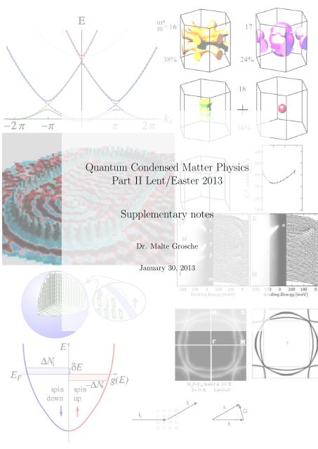
Quantum Condensed Matter Physics<br />
Part II Lent/Easter 2013<br />
Supplementary <strong>notes</strong><br />
Dr. Malte Grosche<br />
January 30, 2013
Contents<br />
1 Classical models for electrons in solids 9<br />
1.1 Lorentz oscillator model . . . . . . . . . . . . . . . . . . . . . . . . . . . . . . . 9<br />
1.2 Drude model . . . . . . . . . . . . . . . . . . . . . . . . . . . . . . . . . . . . . 13<br />
2 Sommerfeld theory 23<br />
2.1 The problems with Drude theory . . . . . . . . . . . . . . . . . . . . . . . . . . 23<br />
2.2 Free electron gas in three-dimensions . . . . . . . . . . . . . . . . . . . . . . . . 24<br />
2.3 Fermi surface, and density <strong>of</strong> states . . . . . . . . . . . . . . . . . . . . . . . . . 25<br />
2.4 Thermal properties <strong>of</strong> the electron gas . . . . . . . . . . . . . . . . . . . . . . . 26<br />
2.5 Screening and Thomas-Fermi theory . . . . . . . . . . . . . . . . . . . . . . . . 27<br />
3 From atoms to solids 33<br />
3.1 The binding <strong>of</strong> crystals . . . . . . . . . . . . . . . . . . . . . . . . . . . . . . . . 33<br />
3.2 Complex matter . . . . . . . . . . . . . . . . . . . . . . . . . . . . . . . . . . . . 37<br />
3.3 The description <strong>of</strong> periodic solids . . . . . . . . . . . . . . . . . . . . . . . . . . 42<br />
3.4 The reciprocal lattice and diffraction . . . . . . . . . . . . . . . . . . . . . . . . 44<br />
3.5 Diffraction conditions and Brillouin zones . . . . . . . . . . . . . . . . . . . . . . 45<br />
3.6 Lattice dynamics and phonons . . . . . . . . . . . . . . . . . . . . . . . . . . . . 48<br />
3.7 Lattice specific heat . . . . . . . . . . . . . . . . . . . . . . . . . . . . . . . . . . 52<br />
4 Electronic structure 55<br />
4.1 Schrödinger equation in a periodic potential . . . . . . . . . . . . . . . . . . . . 55<br />
4.2 Bloch’s theorem from discrete translational symmetry . . . . . . . . . . . . . . . 57<br />
4.3 Nearly free electron theory . . . . . . . . . . . . . . . . . . . . . . . . . . . . . . 60<br />
4.4 Tight binding: Linear combination <strong>of</strong> atomic orbitals . . . . . . . . . . . . . . . 65<br />
4.5 Pseudopotentials . . . . . . . . . . . . . . . . . . . . . . . . . . . . . . . . . . . 71<br />
5 Bandstructure <strong>of</strong> real materials 73<br />
3
4 CONTENTS<br />
5.1 Bands and Brillouin zones . . . . . . . . . . . . . . . . . . . . . . . . . . . . . . 73<br />
5.2 Examples <strong>of</strong> band structures . . . . . . . . . . . . . . . . . . . . . . . . . . . . . 78<br />
5.3 Semiclassical dynamics . . . . . . . . . . . . . . . . . . . . . . . . . . . . . . . . 80<br />
6 Experimental probes <strong>of</strong> the band structure 87<br />
6.1 Optical transitions . . . . . . . . . . . . . . . . . . . . . . . . . . . . . . . . . . 87<br />
6.2 Photoemission . . . . . . . . . . . . . . . . . . . . . . . . . . . . . . . . . . . . . 89<br />
6.3 Quantum oscillations – de Haas van Alphen effect . . . . . . . . . . . . . . . . . 90<br />
6.4 Tunnelling . . . . . . . . . . . . . . . . . . . . . . . . . . . . . . . . . . . . . . . 95<br />
7 Semiconductors 99<br />
7.1 Semiconductor band structure . . . . . . . . . . . . . . . . . . . . . . . . . . . . 99<br />
7.2 Intrinsic carrier concentration . . . . . . . . . . . . . . . . . . . . . . . . . . . . 100<br />
7.3 Doped semiconductors . . . . . . . . . . . . . . . . . . . . . . . . . . . . . . . . 102<br />
8 Semiconductor devices 105<br />
8.1 Metal - semiconductor contact . . . . . . . . . . . . . . . . . . . . . . . . . . . . 105<br />
8.2 p-n junction . . . . . . . . . . . . . . . . . . . . . . . . . . . . . . . . . . . . . . 106<br />
8.3 Solar cell . . . . . . . . . . . . . . . . . . . . . . . . . . . . . . . . . . . . . . . . 111<br />
8.4 Field effect transistor . . . . . . . . . . . . . . . . . . . . . . . . . . . . . . . . . 115<br />
8.5 Compound semiconductor heterostructures . . . . . . . . . . . . . . . . . . . . . 119<br />
9 Electronic instabilities 123<br />
9.1 Charge Density Waves . . . . . . . . . . . . . . . . . . . . . . . . . . . . . . . . 127<br />
9.2 Magnetism . . . . . . . . . . . . . . . . . . . . . . . . . . . . . . . . . . . . . . . 134<br />
10 Fermi liquid theory 145<br />
10.1 The problem with the Fermi gas . . . . . . . . . . . . . . . . . . . . . . . . . . . 145<br />
10.2 Collective excitations . . . . . . . . . . . . . . . . . . . . . . . . . . . . . . . . . 147<br />
10.3 Total energy expansion for Landau Fermi liquid . . . . . . . . . . . . . . . . . . 149<br />
10.4 Fermi liquids at the limit: heavy fermions . . . . . . . . . . . . . . . . . . . . . 154
CONTENTS 5<br />
Preface<br />
Books<br />
There are many good books on solid state and condensed matter physics, but the subject is<br />
rich and diverse enough that each <strong>of</strong> these contains both much more and much less than the<br />
topics covered in this course. The two classic textbooks are Kittel, and Ashcr<strong>of</strong>t and Mermin.<br />
These are both at the correct level <strong>of</strong> the course, and have the virtue <strong>of</strong> clear exposition, many<br />
examples, and lots <strong>of</strong> experimental data. Slightly more concise, though in places a little more<br />
formal is Ziman. Grosso and Parravicini has a somewhat wider coverage <strong>of</strong> material, but much<br />
<strong>of</strong> it goes well beyond the level <strong>of</strong> detail required for this course. Marder is at about the right<br />
level (though again with more detail than we shall need), and has a nice blend <strong>of</strong> quantum<br />
properties with statistical and classical properties. A well illustrated modern treatment <strong>of</strong><br />
most topics in this course is also given by Ibach and Lüth. OUP have recently issued a series <strong>of</strong><br />
short texts in condensed matter physics. They are more detailed than needed for this course,<br />
but are quite accessible and excellent for reference. The most relevant for this course is<br />
Singleton.<br />
• C.Kittel, Introduction to Solid State Physics, 7th edition, Wiley, NY, 1996.<br />
• N.W.Ashcr<strong>of</strong>t and N.D.Mermin, Solid State Physics, Holt-Saunders International Editions,<br />
1976.<br />
• J.M.Ziman, Principles <strong>of</strong> the Theory <strong>of</strong> Solids, CUP, Cambridge, 1972.<br />
• H. Ibach and H. Lüth, Solid State Physics, Springer 1995.<br />
• J. Singleton, Band Theory and the Electronic Properties <strong>of</strong> Solids, OUP 2001.<br />
• M.P. Marder, Condensed Matter Physics, Wiley, NY, 2000. Covers both quantum matter<br />
and mechanical properties.<br />
• G.Grosso and G.P.Parravicini, Solid State Physics, AP, NY, 2000. A wide coverage <strong>of</strong><br />
material, very bandstructure oriented, very detailed.<br />
• A very good book, though with a focus on statistical and “s<strong>of</strong>t” condensed matter that<br />
makes it not so relevant for this course, is<br />
P.M.Chaikin and T.Lubensky, Principles <strong>of</strong> Condensed Matter Physics, CUP, Cambridge,<br />
1995.<br />
These <strong>notes</strong><br />
Treat these <strong>notes</strong> with caution. If you are looking for text book quality, then you should look<br />
at text books.<br />
Polished and optimised treatments <strong>of</strong> most <strong>of</strong> the topics covered here have been published in<br />
a number <strong>of</strong> excellent books, listed above. For much <strong>of</strong> its duration the course follows the book<br />
by Singleton, and where it does not, the books by Ashcr<strong>of</strong>t&Mermin, as well as Kittel, give<br />
essential support. Reading up in text books is not only useful revision <strong>of</strong> the lecture material, it
6 CONTENTS<br />
also serves to give important background information and context, which is difficult to provide<br />
within the scope <strong>of</strong> the lectures. Now that you made it into the second half <strong>of</strong> the third year,<br />
you should really give that a try!<br />
What is the purpose <strong>of</strong> these <strong>notes</strong>, then (i) They may help you to fill in some gaps or<br />
make corrections in your personal lecture <strong>notes</strong>, when the lecture moved too quickly to keep<br />
accurate <strong>notes</strong>. (ii) They may contain some information which was only superficially touched<br />
on during the lectures but not explicitly written down. (iii) They may contain some alternative<br />
approaches, which were not given in the lectures but which may be interesting to know about,<br />
as understanding comes from combining and reconciling many approaches to the same topic.<br />
The <strong>notes</strong> have a complementary function. Do not attempt to learn condensed matter physics<br />
from these <strong>notes</strong> alone. The lectures will be presented using more qualitative and physical<br />
descriptions. In some places, treatments given in the lectures are simpler and more direct than<br />
what you will find in the <strong>notes</strong>. The lecture overheads together with your personal <strong>notes</strong> from<br />
the lectures form the backbone <strong>of</strong> this course – and where they do not suffice, text books and<br />
these <strong>notes</strong> as background reading material may help.<br />
Notation<br />
Material which is explicitly non-examinable is placed in small type. Do not be confused, if<br />
wavevector or frequency dependencies in these <strong>notes</strong> are sometimes expressed in terms <strong>of</strong> subscripts<br />
and sometimes as function arguments. For example ɛ ω = ɛ(ω), and V q = V (q). The<br />
two notations are used interchangeably in this handout.
CONTENTS 7<br />
Outline<br />
“Any new discovery contains the germ <strong>of</strong> a new industry.”<br />
(J. J. Thomson)<br />
In this course, we will take a tentative first step towards working with electrons in solids. This<br />
requires skills you have acquired in other courses, in particular in electromagnetism, quantum<br />
mechanics and statistical physics.<br />
The course is structured as follows: roughly the first half <strong>of</strong> Lent term consists <strong>of</strong> a progression<br />
<strong>of</strong> more and more sophisticated models, each fixing the deficiencies <strong>of</strong> its predecessor. We<br />
will start by considering electrons in insulators (Lorentz oscillator model) and metals (Drude<br />
model) by very intuitive classical approaches, which get quite a number <strong>of</strong> things right. We<br />
will then introduce quantum statistics (Sommerfeld model) to correct those things which go<br />
most spectacularly wrong in the classical approach. We will then introduce the crystalline<br />
lattice, which the Sommerfeld model does not take into account, and ponder its symmetry<br />
properties and its vibrations. Arguably the toughest point <strong>of</strong> the course is the introduction<br />
<strong>of</strong> Bloch’s theorem and the calculation <strong>of</strong> electronic energy levels (or band structure) in the<br />
presence <strong>of</strong> a periodic potential caused by the lattice atoms. This is done in two ways, (i)<br />
using the nearly free electron gas approach, and (ii) using linear combination <strong>of</strong> atomic orbitals<br />
(or tight binding), which is technically easier. Having reached this point, it is downhill again,<br />
considering band structures <strong>of</strong> real materials and how band structures can be determined experimentally.<br />
Lent term will conclude with an introduction to how all <strong>of</strong> this can be applied to<br />
build semiconductor-based devices.<br />
The models discussed up to this point in the course neglect correlations between the electrons:<br />
having computed the single-electron energy eigenstates <strong>of</strong> a solid, we then fill up these<br />
states with the available electrons, ignoring the mutual interaction between the electrons. We<br />
will apply these models in order to understand semiconductor-based electronic devices such as<br />
p-n junction based diodes, field effect transistors and solar cells.<br />
Because the mobile electrons are strongly diluted in semiconductors, neglecting the effects<br />
<strong>of</strong> the mutual repulsion between the electrons can be justified. This can be very different<br />
in metals, however, which can be regarded as dense electron liquids. We find that in many<br />
metals, the strong electron-electron interaction can cause new collective phenomena. The most<br />
prominent examples are magnetism, <strong>of</strong> which there are many varieties, and superconductivity,<br />
but there are many other possible forms <strong>of</strong> electronic quantum self-organisation. We will take a<br />
first step towards understanding the driving force behind such collective states by considering<br />
charge and spin instabilities in metals, and we will discuss a very general conceptual framework<br />
for working with strongly interacting fermionic systems, in many ways the standard model <strong>of</strong><br />
condensed matter physics, namely Landau’s Fermi liquid theory.
8 CONTENTS
Chapter 1<br />
Classical models for electrons in solids<br />
We will start out by considering intuitive, classical models for condensed matter, which were<br />
first put forward in the late 19th century. These models are the Lorentz, or dipole oscillator<br />
model, in which the oscillations <strong>of</strong> charges around their average positions is incorporated, and<br />
the Drude model, in which electrons are treated similarly to an ideal gas.<br />
As the shortcomings <strong>of</strong> these models become apparent, we will progress to more sophisticated<br />
models. In particular, we find that electrons form a degenerate quantum gas, in which states<br />
are occupied according to the Pauli exclusion principle. This leads to the Sommerfeld model<br />
<strong>of</strong> the free electron gas. Next, we will consider the effect <strong>of</strong> the periodic potential produced by<br />
the lattice atoms on the electronic states. This leads to the full electronic band structure and<br />
the possibility <strong>of</strong> producing energy gaps. Finally, in the Easter term, we will begin to include<br />
the effects <strong>of</strong> interactions between the electrons.<br />
For now, however, we concentrate on how the electromagnetic response <strong>of</strong> an insulator would<br />
have been modelled using classical physics ...<br />
1.1 Lorentz oscillator model<br />
We consider the effect <strong>of</strong> incoming electromagnetic waves on the charges present in an insulator.<br />
For frequencies up to far above the optical range, the wavelengths are much larger than the<br />
separation between the atoms, so we are effectively in the long wavelength limit and can assume<br />
that the electric field across a single atom is uniform.<br />
We model the atoms as consisting <strong>of</strong> a positively charged nucleus and a negatively charged<br />
electron cloud. An applied electric field causes displacement <strong>of</strong> electron cloud by distance u.<br />
For small displacements, we can linearise the restoring force and assume that the restoring force<br />
is proportional to the displacement. This leads to modelling the electron cloud as a damped<br />
harmonic oscillator,<br />
mü + mγ ˙u + mω 2 T u = qE , (1.1)<br />
where q is the electron’s charge (= −e), ω T represents the natural frequency, given by<br />
force constant and mass, and γ is a damping rate. Within our classical model, it is difficult<br />
to attribute γ quantitatively to an actual physical damping mechanism – we might think <strong>of</strong><br />
radiative losses or interference with the electron clouds on neighbouring atoms – but even if<br />
9
10 CHAPTER 1. CLASSICAL MODELS FOR ELECTRONS IN SOLIDS<br />
Electron cloud,<br />
mass m, charge q<br />
u<br />
Electron cloud oscillates<br />
about nucleus,<br />
displacement = u<br />
Nucleus<br />
u<br />
.<br />
Figure 1.1: Classical picture <strong>of</strong> the electron cloud oscillating around a stationary ion<br />
we do not have a theory to calculate γ, we can have it in our model as a phenomenological<br />
parameter.<br />
In the presence <strong>of</strong> an oscillating electric field E(t) = E ω e −iωt , the electron cloud will oscillate<br />
with a displacement u(t) = u ω e −iωt . The resulting dipole moment per atom at angular frequency<br />
ω is p ω = qu ω , and this gives rise to a polarisation (=dipole moment density) P ω = ɛ 0 χ ω E ω ,<br />
where the polarisability χ ω is obtained from the equation <strong>of</strong> motion (1.1) as<br />
χ ω = N V<br />
q 2<br />
mɛ 0 (ω 2 T − ω2 − iωγ)<br />
, (1.2)<br />
where N/V is the number density <strong>of</strong> dipoles.<br />
The relative permittivity is ɛ ω = 1 + χ ω . The typical frequency dependence <strong>of</strong> the permittivity<br />
is illustrated in Fig. 1.2.<br />
The analogy with a damped harmonic oscillator tells us that the power absorbed by the<br />
electron cloud is determined by the imaginary part <strong>of</strong> ɛ: it is 1 2 ωɛ 0|E ω | 2 Im(ɛ ω ). This is a simple<br />
way to think about absorption lines in optical spectra and the origin <strong>of</strong> colours.<br />
Also, note that the presence <strong>of</strong> a resonance at higher frequency makes itself felt even well<br />
below the resonance frequency. In the low frequency limit it causes an enhancement <strong>of</strong> the<br />
permittivity:<br />
ɛ(ω → 0) = 1 + N V<br />
q 2<br />
mɛ 0 ω 2 T<br />
This helps us understand why different materials can have very different static (low frequency)<br />
permittivities. Moreover, a mismatch in dielectric permittivity between two media<br />
gives rise to reflection. We write the reflectivity at the interface between two media, if the<br />
permeability µ is the same in both media, as<br />
(1.3)<br />
r =<br />
and the power reflection coefficient as R = |r| 2 .<br />
√<br />
ɛ1 − √ ɛ 2<br />
√<br />
ɛ1 + √ ɛ 2<br />
, (1.4)
1.1. LORENTZ OSCILLATOR MODEL 11<br />
Im(ε)<br />
Permittivity ε<br />
1<br />
0<br />
Re(ε)<br />
0 ω Τ<br />
Frequency<br />
Figure 1.2: Real and imaginary part <strong>of</strong> the relative permittivity within the Lorentz (or dipole)<br />
oscillator model. Note that ɛ = χ + 1 and the polarisability χ ω has the frequency dependence<br />
typical for a damped harmonic oscillator.<br />
Note: we need to be careful with taking the Lorentz oscillator model at face value. Our calculation is not<br />
yet fully self-consistent, because the electric field experienced by the electron cloud on one atom is not only the<br />
applied field; it is also modified by the polarisation and the associated electric field caused by other atoms in<br />
the vicinity. It can be shown, but it is outside the scope <strong>of</strong> this course, that the resulting corrections do not<br />
change the functional form <strong>of</strong> ɛ ω but rather shift the apparent resonance frequencies ω T from those expected<br />
purely from atomic parameters such as the effective spring constant and electronic mass. In short, while the<br />
above treatment is correct for dilute gases, it needs to be modified for solids, but these modifications do not<br />
change the overall form <strong>of</strong> the results.<br />
Of course, this classical model cannot be the whole story. For example, the equipartition<br />
theorem would tell us that each dipole oscillator should contribute 2× 1k 2 B to the heat capacity <strong>of</strong><br />
the solid, when measurements show that the contribution due to the electrons in an insulator is<br />
vanishingly small. Also, the model gives us no handle on calculating the resonance frequencies.<br />
It works, however, as a phenomenological description <strong>of</strong> the optical response functions. Fig. 1.3<br />
explains why: For two sharply defined energy levels E a and E b , time-dependent perturbation<br />
theory gives χ ω ∝ (E b −E a −h¯ω) −1 +2πiδ(E b −E a −h¯ω). The imaginary part in this expression<br />
1<br />
corresponds to the transition rate. This expression can also be written as χ ω ∝<br />
E b −E a−h¯ω−ih¯γ/2<br />
with infinitesimal γ. As the energy levels broaden into bands, causing γ to become finite,<br />
this expression becomes similar to the Lorentz model close to the resonance frequency ω T =<br />
ω<br />
(E b − E a )/h¯, if we multiply top and bottom by ω T + ω: χ ω ∝<br />
T +ω<br />
≃ 2ω T<br />
, if<br />
ωT 2 −ω2 −i(ω T +ω)γ/2 ωT 2 −ω2 −iωγ<br />
we approximate ω by ω T where the sum, not the difference <strong>of</strong> the two frequencies occurs.<br />
In general, atomic spectra can give rise to multiple allowed transitions at energies h¯ω T 1 ,<br />
h¯ω T 2 , ... , h¯ω T i , etc. Usually, these occur at high frequency, at least in the optical range. The<br />
resulting frequency-dependent permittivity can be obtained by adding the responses associated<br />
with each transition: ɛ(ω) = 1 + ∑ χ i (ω) (Fig. 1.4)
12 CHAPTER 1. CLASSICAL MODELS FOR ELECTRONS IN SOLIDS<br />
|b><br />
|b><br />
|a><br />
ħω T<br />
atomic levels<br />
broaden<br />
|a><br />
Absorption<br />
line<br />
Absorption<br />
peak<br />
ω T<br />
ω<br />
ω T<br />
ω<br />
Figure 1.3: Absorption spectra produced by electronic transitions in atoms (discrete levels) and<br />
solids (levels are broadened). In solids, the sharp absorption peaks found in atomic spectra<br />
broaden out into resonances with a finite width. The resulting absorption spectra have a similar,<br />
Lorentzian form to that expected from the dipole oscillator model<br />
Im(ε)<br />
Permittivity ε<br />
Re(ε)<br />
ε static<br />
1<br />
0<br />
0 ω T1 ω T2 ω T3<br />
Frequency<br />
Figure 1.4: The electromagnetic response <strong>of</strong> an insulator can very generally be modelled by<br />
superimposing dipole oscillator responses with different natural frequencies, each scaled by a<br />
suitable oscillator strength. The low frequency, static permittivity then includes contributions<br />
from the low frequency tails <strong>of</strong> all the individual oscillator responses.
1.2. DRUDE MODEL 13<br />
Im(ε)<br />
Permittivity ε<br />
0<br />
Re(ε)<br />
0 ω p<br />
*<br />
Frequency<br />
Figure 1.5: Real and imaginary part <strong>of</strong> the dielectric permittivity in the Drude model. The<br />
peak at ω T1 illustrates the possibility <strong>of</strong> additional resonances due to the bound, core electrons.<br />
1.2 Drude model<br />
The Lorentz, or dipole oscillator model extends naturally to metals, if we imagine that some<br />
<strong>of</strong> the electrons are no longer bound to the ions. The remaining inner, or core electrons are<br />
still closely bound and will continue to contribute to the permittivity according to the Lorentz<br />
oscillator model. The outer, or conduction electrons, however, have been cut loose from the<br />
ions and are now free to roam around the entire piece <strong>of</strong> metal. This corresponds to the<br />
spring constant in their linearised force law going to zero, and hence the natural frequency ω T<br />
vanishes. To model their contribution to ɛ ω we can then simply use our earlier expressions for<br />
the frequency dependent permittivity, but drop ω T : the resonance peak now occurs at zero<br />
frequency. This picture, in which some <strong>of</strong> the electrons are cut free from the ionic cores, is<br />
called the Drude model.<br />
ω T1<br />
1.2.1 Optical properties <strong>of</strong> metals in the Drude model<br />
<strong>Set</strong>ting ω T in the dipole oscillator response (1.2) to zero and inserting a background permittivity<br />
ɛ ∞ to take account <strong>of</strong> the polarisability <strong>of</strong> the bound core electrons, leads us to the Drude<br />
response<br />
ɛ ω = ɛ ∞ − N V<br />
q 2<br />
mɛ 0 (ω 2 + iωγ) = ɛ ∞ −<br />
ω 2 p<br />
ω 2 + iωγ<br />
, (1.5)<br />
where ωp 2 = ne2<br />
mɛ 0<br />
(defining n = N/V , the number density <strong>of</strong> mobile electrons). ω p is called the<br />
plasma frequency.<br />
We can draw three immediate conclusions from the above form <strong>of</strong> the permittivitiy (Fig. 1.2):<br />
1. |ɛ ω | diverges for ω → 0 =⇒ metals are highly reflecting at low frequency.<br />
2. The imaginary part <strong>of</strong> ɛ ω peaks at ω = 0, giving rise to enhanced absorption at low<br />
frequency, the ’Drude peak’.<br />
3. ɛ ω crosses through zero at high frequency ωP ∗ =⇒ metals become transparent in the<br />
ultraviolet.
14 CHAPTER 1. CLASSICAL MODELS FOR ELECTRONS IN SOLIDS<br />
1<br />
Power reflection coeff. |r| 2<br />
ε ∞ = 5<br />
background permittivity ε ∞ = 1<br />
(ω p /ω)**4<br />
0<br />
*<br />
0 ω p<br />
ω p<br />
Frequency<br />
Figure 1.6: Frequency dependence <strong>of</strong> the power reflection coefficient R = |r| 2 in the Drude<br />
model.<br />
Moreover, the reflection coefficient at an air/metal interface has an interesting frequency<br />
dependence. Substituting the Drude form for ɛ ω into Eq. 1.4 allows us to analyse this in<br />
some detail (see question on problem sheet 1). We find that the power reflection coefficient R<br />
reaches 1 in the limit ω → 0, then assumes a weakly frequency dependent value less than 1<br />
over a wide frequency range, and drops <strong>of</strong>f as R ∝ ω −4 at high frequency. A finite background<br />
polarisability (caused by the core electrons), which gives rise to ɛ ∞ > 1 causes R to dip to zero<br />
at finite frequency (Fig. 1.6).<br />
1.2.2 Plasma oscillations<br />
These results are directly analogous to some <strong>of</strong> those seen in the Part 1B Electromagnetism<br />
course on the topic <strong>of</strong> plasmas. According to the Drude model, electrons in metals behave<br />
like a plasma, i.e. a classical charged gas moving in an oppositely charged environment. The<br />
electrons act in many ways like an ideal gas, but whereas the molecules <strong>of</strong> an ideal gas are meant<br />
to scatter <strong>of</strong>f each other, we take the electrons as completely non-interacting. Our electrons<br />
do scatter <strong>of</strong>f defects in the solid, however, which includes thermally excited lattice vibrations<br />
(phonons), and this gives them a mean free path l and a scattering rate, which is the inverse <strong>of</strong><br />
the relaxation time τ. We assume that a scattering event completely randomises an electron’s<br />
momentum. As will be explained in more detail below, we can identify the damping rate γ in<br />
Eq. 1.5 with the scattering rate τ −1 .<br />
One <strong>of</strong> the findings <strong>of</strong> the Part 1B Electromagnetism course was the occurrence <strong>of</strong> plasma<br />
oscillations. That there should be free oscillations in the plasma is surprising at first, because<br />
we have reduced the restoring force due to the ionic cores to zero (ω T → 0) to obtain the Drude<br />
model. Where could these oscillations come from<br />
Consider probing a slab <strong>of</strong> material (the sample) by applying an oscillating field (see<br />
Fig. 1.7). The free charges brought into the vicinity <strong>of</strong> our sample to probe its properties<br />
produce a displacement, or D− field. Because D ⊥ is continuous across the interface, this can<br />
be translated to the electric field, or E−field inside the sample, and the polarisation P can be<br />
determined:
1.2. DRUDE MODEL 15<br />
!<br />
#<br />
"<br />
Figure 1.7: Exciting plasma oscillations by applying an oscillating electric field<br />
ɛ 0 E = ɛ −1 D = D − P<br />
=⇒ P = D(1 − ɛ −1 )<br />
Hence, the response to an oscillating applied D-field is given by ɛ −1 , which we can compute<br />
from (1.5). In metals, ω p >> γ = τ −1 and usually ɛ ∞ ≃ 1. In this case, we can write 1/ɛ as<br />
ɛ(ω) −1 =<br />
ω2 + iωγ<br />
ω 2 − ω 2 p + iωγ<br />
(1.6)<br />
(remember that ωp 2 = ne2<br />
mɛ 0<br />
, where we define n = N/V ).<br />
We see that for ɛ ∞ = 1, the inverse permittivity 1/ɛ ω peaks at the plasma frequency:<br />
ɛ(ω p ) → 0. More generally, ɛ → 0 at ωp ∗ = ω p / √ ɛ ∞ . This implies (because D = ɛ 0 ɛ ω E) a finite<br />
amplitude <strong>of</strong> oscillation for E and P despite zero forcing field D, so that at ω = ωp ∗ (’Plasma<br />
frequency’), the polarisation can oscillate without even having to apply a driving field. These<br />
are modes <strong>of</strong> free oscillation: solutions <strong>of</strong> the form u 0 e −iωpt with high resonance frequency<br />
corresponding to energies in the eV range. This free resonance <strong>of</strong> the conduction electrons<br />
on top <strong>of</strong> the positively charged ionic charge background is called a plasma oscillation. Any<br />
polarisation in the metal causes surface charges to build up, which generate a restoring force<br />
that can drive oscillations. The entire electron gas in the metal oscillates back and forth in<br />
synchrony. The peak width <strong>of</strong> this resonance is given by τ −1 .<br />
Plasma oscillations can be detected by measurements <strong>of</strong> the optical absorption (which give<br />
us Im(ɛ ω )), or they can be probed by inelastic scattering <strong>of</strong> charged particles such as electrons.<br />
When high energy electrons pass through the metal, they can excite plasma oscillations and<br />
thereby lose some <strong>of</strong> their energy. By comparing incident and final energies, we can deduce the<br />
energy <strong>of</strong> the plasma oscillations. This is called Electron Energy Loss Spectroscopy (EELS). As<br />
in any driven oscillator, energy is dissipated at or near the resonant frequency (with the width<br />
in frequency depending on the damping <strong>of</strong> the oscillator). An EELS spectrum will therefore<br />
have a peak near the plasma frequency (Fig. 1.8).
16 CHAPTER 1. CLASSICAL MODELS FOR ELECTRONS IN SOLIDS<br />
Figure 1.8: Detection <strong>of</strong> plasma oscillations by electron energy loss spectroscopy. Left panel:<br />
Generic diagram <strong>of</strong> an inelastic scattering experiment. The incident particle – in this case an<br />
electron – is scattered to a final state <strong>of</strong> different energy and momentum. Electrons enter the<br />
sample at wavevector q and energy h¯ω. The outgoing electrons have a different wavevector<br />
k and energy h¯ν. By comparing the incident and scattered energies, one deduces the energy<br />
loss spectrum <strong>of</strong> the internal collective excitations in the medium. For high energy electrons<br />
- typically used in an EELS experiment - the momentum loss (q − k) is small. Centre and<br />
right panels: Electron energy loss spectrum for Ge and Si (dashed lines) compared to values <strong>of</strong><br />
Im(1/ɛ) extracted directly from measurements <strong>of</strong> the optical absorption. The energy difference<br />
between incoming and outgoing electrons is attributed to the excitation <strong>of</strong> plasma oscillations<br />
(or ’plasmons’) with energy h¯(ω − ν). [From H.R.Philipp and H.Ehrenreich, Physical Review<br />
129, 1550 (1963)<br />
1.2.3 Frequency dependent conductivity in the Drude model<br />
What we have done so far in order to work out the frequency dependent permittivity in metals<br />
was to start with the Lorentz oscillator model and simply put the dipole resonance frequency<br />
ω T to zero. This approach could be seen as conceptually somewhat unsatisfactory, primarily<br />
for two reasons:<br />
1. If the electrons are cut loose from the ionic cores, their average position, around which<br />
they are meant to oscillate, is no longer defined. The displacement u for an individual<br />
electron acquires an arbitrary <strong>of</strong>fset.<br />
2. Our picture for scattering processes (electrons occasionally hit an obstacle and thereby<br />
randomise their momentum) prevents us from ascribing the same velocity to all the electrons<br />
– we need a statistical description.<br />
These issues can be addressed by two modifications to our approach, which do not change<br />
any <strong>of</strong> our results so far, but help us interpret these results and make further progress:
1.2. DRUDE MODEL 17<br />
1. Rather than starting with an equation <strong>of</strong> motion for the electronic displacement, we<br />
consider the rate <strong>of</strong> change <strong>of</strong> the velocity v = ˙u.<br />
2. Instead <strong>of</strong> considering the velocity <strong>of</strong> an individual electron, we average over a large<br />
number electrons, and look for a differential equation for the average velocity <strong>of</strong> the<br />
electrons. Even if the individual electrons have wildly different velocities, the average, or<br />
drift velocity will be seen to follow a simple equation <strong>of</strong> motion, and it is the drift velocity<br />
which determines the optical and transport properties <strong>of</strong> the metal.<br />
Writing ρ = qN/V for the charge density, we can express the current density j in terms <strong>of</strong><br />
the average velocity v <strong>of</strong> the mobile, or conduction electrons, and we can link j to E via the<br />
conductivity σ and Ohm’s law:<br />
j = ρv = σE (1.7)<br />
Because the polarisation P = (N/V )uq, we can link the current density to the timederivative<br />
<strong>of</strong> the polarisation due to the conduction electrons, P c :<br />
j = Ṗc (1.8)<br />
Note that while there can be some ambiguity about P due to the ambiguity about the<br />
displacement u for travelling electrons, this drops out <strong>of</strong> the time derivative, so the expression<br />
for j is correct. 1<br />
Adding in the polarisation <strong>of</strong> the core electrons, which is given by the background polarisability<br />
χ ∞ , we obtain<br />
Ṗ = j + ɛ 0 χ ∞ Ė (1.9)<br />
Considering, as before, the oscillatory response v ω e −iωt , j ω e −iωt , P ω e −iωt to an oscillating<br />
electric field E ω e −iωt , we find for the Fourier components<br />
from which we obtain the key expressions<br />
j ω = σ ω E ω = −iωɛ 0 (χ ω − χ ∞ )E ω , (1.10)<br />
σ ω = −iωɛ 0 (ɛ ω − ɛ ∞ )<br />
ɛ ω = i σ ω<br />
ɛ 0 ω + ɛ ∞ (1.11)<br />
These expressions relate the imaginary part <strong>of</strong> the permittivity (which determines optical<br />
absorption) to the real part <strong>of</strong> the frequency dependent conductivity. That means that we can<br />
indirectly determine the conductivity <strong>of</strong> a metal at high frequencies by optical measurements.<br />
If the atomic (or background) polarisability is zero, then ɛ ∞ = 1 and σ ω = −iωɛ 0 (ɛ ω − 1).<br />
1 An alternative approach, which avoids introducing the field u(r, t) altogether, could consider ∇P c = −ρ c<br />
and ˙ρ c = −∇j to find j = Ṗc + j 0 , where ∇j 0 = 0 so that the boundary conditions on the sample fix j 0 = 0.
18 CHAPTER 1. CLASSICAL MODELS FOR ELECTRONS IN SOLIDS<br />
Differential equation for the drift velocity<br />
Rather than simply inserting our earlier expression (1.5) into (1.11), which would indeed give us<br />
a correct expression for the frequency dependent conductivity σ ω within the Drude model, we<br />
can also derive an expression for σ ω by considering an equation <strong>of</strong> motion for the drift velocity<br />
<strong>of</strong> the electrons, or for the resulting current density. This answers the conceptual issues raised<br />
earlier and gives a more precise meaning to the relaxation time τ. The drift velocity relates to<br />
the total momentum <strong>of</strong> the electron system via v =<br />
p , where N is the number <strong>of</strong> electrons<br />
Nm<br />
in the system and m is the electron mass. The momentum, in turn, changes in the presence <strong>of</strong><br />
an applied electric or magnetic field. If there were no collisions, which can remove momentum<br />
from the electron system, then we would have ṗ = Nf(t) = N q (E + v × B).<br />
m<br />
Collisions, or scattering, will introduce a further term, which represents the decay <strong>of</strong> the<br />
electron momentum in the absence <strong>of</strong> an external force. Note that electron-electron collisions<br />
do not give rise to a decay <strong>of</strong> momentum in any obvious way: they would appear to conserve<br />
the momentum <strong>of</strong> the electron system. It turns out that at a more advanced level <strong>of</strong> analysis,<br />
they do contribute to the relaxation <strong>of</strong> momentum, but let us for the moment neglect this<br />
contribution. The electron momentum decays, then, because <strong>of</strong> collisions <strong>of</strong> the electrons with<br />
lattice imperfections, such as impurities, dislocations etc., and – in the wider sense – lattice<br />
distortions caused by lattice vibrations.<br />
We could model the influence <strong>of</strong> electron scattering events by making two very simplifying<br />
assumptions:<br />
• Electron collisions randomise an electron’s momentum, so that – on average – the contribution<br />
<strong>of</strong> an electron to the total momentum is 0 after a collision.<br />
• The probability for a collision to occur, P , is characterised by a single relaxation time τ:<br />
P (collision in [t, t + dt]) = dt/τ.<br />
From these assumptions, we find that the probability that a particular electron has not<br />
scattered in the time interval [t, t + dt] is 1 − dt/τ. As only the electrons which have not<br />
scattered contribute to the total momentum (the momentum <strong>of</strong> the others randomises to zero<br />
on average), and these electrons continue to be accelerated by the applied force, we obtain a<br />
total momentum after time t + dt:<br />
p(t + dt) = (1 − dt/τ)(p(t) + Nf(t)dt) + ... (1.12)<br />
This gives rise to a differential equation for the momentum:<br />
( d<br />
dt + 1 τ<br />
)<br />
p = Nf(t) (1.13)<br />
and, substituting f = qE, we obtain for the drift velocity and for the current density:<br />
( d<br />
dt + 1 τ<br />
)<br />
( d<br />
dt + 1 τ<br />
)<br />
j = N V<br />
v = q (E + v × B)<br />
m<br />
q 2<br />
m E(t) + q m j × B (1.14)
1.2. DRUDE MODEL 19<br />
We neglect B for the time being, as the effects <strong>of</strong> the magnetic field accompanying an e-m<br />
wave on the electron system are much weaker than those <strong>of</strong> the electric field. However, B will<br />
be included in transport phenomena at low frequencies, below (Hall effect). Then, we obtain<br />
the simplified equations<br />
( d<br />
dt + 1 τ<br />
)<br />
v = qE(t)/m<br />
( d<br />
dt + 1 τ<br />
)<br />
j = N V<br />
q 2<br />
E(t) (1.15)<br />
m<br />
To extract the frequency dependent conductivity from (1.15), we again insert a trial solution<br />
<strong>of</strong> the form j = j ω e −iωt and a time-varying field <strong>of</strong> the form E = E ω e −iωt . This transforms the<br />
above differential equation into an algebraic equation:<br />
j ω = ne2<br />
m<br />
1<br />
1/τ − iω E ω (1.16)<br />
(remember that q = −e is the electron’s charge, and we write the number density N/V as<br />
n). Using the definition <strong>of</strong> the conductivity j = σE, we obtain:<br />
σ ω = ne2<br />
m<br />
1<br />
1/τ − iω , (1.17)<br />
In the low frequency limit, this expression for the conductivity tends to the DC conductivity<br />
σ 0 = ne2 τ<br />
m<br />
At frequencies larger than 1/τ the conductivity falls <strong>of</strong>f rapidly:<br />
(1.18)<br />
Re(σ ω ) =<br />
σ(0)<br />
1 + ω 2 τ 2 . (1.19)<br />
The DC (ω = 0) conductivity can also be written in terms <strong>of</strong> the mobility µ = eτ/m<br />
σ = neµ = ne2 τ<br />
m<br />
(1.20)<br />
Inserting (1.17) into Eqn. 1.11 gives<br />
ɛ(ω) = ɛ ∞ −<br />
ω 2 p<br />
ω 2 + iω/τ<br />
, (1.21)<br />
which is exactly the expression we obtained right at the start (Eq. 1.5) by setting ω T → 0,<br />
if we identify 1/τ with γ. Here, as before, ω p is the Plasma frequency:<br />
ω 2 p = ne2<br />
ɛ 0 m<br />
(1.22)
20 CHAPTER 1. CLASSICAL MODELS FOR ELECTRONS IN SOLIDS<br />
1.2.4 Low frequency (DC) transport properties in the Drude model<br />
We now use the differential equation we obtained earlier for the current density in applied<br />
electric and magnetic fields, (1.14), in order to study the electrical transport in a transverse<br />
magnetic field. We consider an arrangement, in which a static magnetic field B is applied along<br />
the ẑ direction, and static currents and electrical fields are constrained to the x − y plane.<br />
The equations <strong>of</strong> motion for charge carriers with charge q are now 2 .<br />
(<br />
∂t + τ −1) j x = q2 n<br />
m (E x + v y B)<br />
(<br />
∂t + τ −1) j y = q2 n<br />
m (E y − Bv x ) (1.23)<br />
(<br />
∂t + τ −1) j z = q2 n<br />
m E z<br />
In steady state , we set the time derivatives ∂ t = d/dt = 0, and get the three components<br />
<strong>of</strong> the current density<br />
( qτ<br />
)<br />
j x = qn<br />
m E x + βv y<br />
( qτ<br />
)<br />
j y = qn<br />
m E y − βv x (1.24)<br />
j z = qn qτ m E z<br />
with the dimensionless parameter β = qB m τ = ω cτ = µB the product <strong>of</strong> the cyclotron<br />
frequency (ω c = qB/m) and the relaxation time, or <strong>of</strong> the mobility and the applied field.<br />
Hall effect<br />
Consider now the rod-shaped geometry <strong>of</strong> Fig. 1.9. The current is forced by geometry to flow<br />
only in the x-direction, and so j y = 0, v y = 0. Since there is no flow in the normal direction,<br />
there must be an electric field E = −v × B, which exactly counterbalances the Lorentz force<br />
on the carriers. This is the Hall effect. We find<br />
and<br />
v x = qτ m E x , (1.25)<br />
E y = βE x (1.26)<br />
(remember β = qB τ). It turns out that for high mobility materials, and large magnetic<br />
m<br />
fields, it is not hard to reach large values <strong>of</strong> |β| ≫ 1, so that the electric fields are largely<br />
normal to the electrical currents.<br />
2 Again, we define e to be the magnitude <strong>of</strong> the charge <strong>of</strong> an electron. Note, also, that the particle mass m,<br />
may in general differ from the mass <strong>of</strong> an electron in vacuum, m e . We will see later that in solids the effective<br />
charge carrier mass depends on details <strong>of</strong> the electronic structure.
1.2. DRUDE MODEL 21<br />
Figure 1.9: The upper figure shows the geometry <strong>of</strong> a Hall bar, with the current flowing<br />
uniformly in the x-direction, and the magnetic field in z. The lower figure shows the steady<br />
state electron flow (arrows) in a section normal to ẑ. When a voltage E x is first applied, and E y<br />
is not yet established, the electrons will deflect and move in the (downward) y-direction. The<br />
y-surfaces <strong>of</strong> the crystal then become charged, producing the field E y which exactly cancels the<br />
Lorentz force −ev x B.<br />
The Hall coefficient is defined by<br />
R H = E y<br />
j x B = 1 nq<br />
(1.27)<br />
Notice that it is negative for electrons, but importantly is independent <strong>of</strong> the effective mass,<br />
and grows with decreasing carrier density. For holes <strong>of</strong> charge +e the sign is positive.<br />
The Hall effect is an important diagnostic for the density and type <strong>of</strong> carriers transporting<br />
the electrical current in a semiconductor. The simple picture presented here works quite well<br />
for alkali metals, where the predicted Hall coefficient is within a few percent <strong>of</strong> the expected<br />
value for a parabolic free electron band. But Be, Al, and In all have positive Hall coefficients<br />
- accounted for by a band-structure with hole pockets that dominates the Hall effect. In more<br />
complicated cases, still, contributions from both positive and negative carriers, attributed to<br />
different electronic bands, combine in a non-trivial way to determine the Hall effect.<br />
Thermal conductivity <strong>of</strong> metals<br />
Particles with velocity v, mean free path l and specific heat C are expected to yield a thermal conductivity<br />
K = Cvl/3. For a free fermi gas, we get the correct answer from this formula by using the electronic<br />
specific heat, the characteristic carrier velocity v F , and the mean free path for carriers on the fermi surface<br />
l = v F τ. Hence, using the relationship between the Fermi velocity and the Fermi energy E F = mv 2 F /2,<br />
K el = π2<br />
2<br />
nk 2 B T<br />
E F<br />
· v F · v F τ = π2 nk 2 B T τ<br />
3m<br />
(1.28)<br />
Almost invariably, the electronic thermal conductivity is bigger than that due to the lattice. K and σ<br />
are <strong>of</strong> course closely related, being both proportional to the scattering time and the density, as is natural.
22 CHAPTER 1. CLASSICAL MODELS FOR ELECTRONS IN SOLIDS<br />
The ratio<br />
(<br />
K<br />
σT = π2 kB<br />
3 e<br />
) 2<br />
(1.29)<br />
is expected to be a constant, independent <strong>of</strong> material parameters.<br />
Wiedemann-Franz law, which works strikingly well for simple metals.<br />
This proportionality is the<br />
1.2.5 Summary <strong>of</strong> key results in Drude theory<br />
Plasma frequency<br />
ω 2 p = ne2<br />
ɛ 0 m<br />
Frequency dependence <strong>of</strong> the relative permittivity and <strong>of</strong> the electrical conductivity (taking<br />
into account the polarisability <strong>of</strong> the atomic cores, χ ∞ = ɛ ∞ − 1 causes slight modifications):<br />
ɛ(ω) = 1 −<br />
ω 2 p<br />
ω 2 + iωγ<br />
ɛ ∞≠1<br />
−−−→ ɛ ∞ −<br />
ω 2 p<br />
ω 2 + iωγ<br />
σ(ω) = −iωɛ 0 (ɛ(ω) − 1) ɛ∞≠1<br />
−−−→ −iωɛ 0 (ɛ(ω) − ɛ ∞ )<br />
Useful expressions for electrical conductivity and Hall coefficient:<br />
σ(ω) =<br />
ne 2 τ<br />
m(1 − iωτ)<br />
ω→0<br />
−−→ ne2 τ<br />
m<br />
= neµ<br />
R H = 1 nq<br />
(q is carrier charge, n is carrier density, τ is relaxation time = 1/γ)
Chapter 2<br />
Sommerfeld theory – electrons as a<br />
degenerate quantum gas<br />
2.1 The problems with Drude theory<br />
Just as the Lorentz oscillator model is successful at describing the optical response <strong>of</strong> insulators,<br />
Drude theory works surprisingly well in modelling the optical and transport properties<br />
<strong>of</strong> metals. Both theories fail dramatically, however, when the thermodynamic properties are<br />
considered. Applying the equipartition theorem to the dipole oscillator model, we would expect<br />
a contribution <strong>of</strong> k B to the heat capacity <strong>of</strong> each oscillator. Similarly, within the Drude model,<br />
which treats the conduction electrons like a classical ideal gas, we would expect a contribution<br />
to the heat capacity <strong>of</strong> 3 2 k B per conduction electron. In reality, the measured heat capacities<br />
for both insulators and metals are far beyond those values (Fig. 2.1).<br />
The reason for this is the same as the reason why the heat capacity due to lattice vibrations<br />
falls below the Dulong-Petit limit at low temperature: electronic motion is largely frozen out,<br />
because in a quantum mechanical model for the electrons, the energy required to excite them<br />
exceeds the thermal energy available.<br />
More specifically, in insulators, the atomic energy levels are separated by large energy gaps<br />
<strong>of</strong> the order <strong>of</strong> electron Volts (≃ k B × 11, 000 K). Therefore, the specific heat contribution due<br />
to electronic excitations in insulators will only become noticeable at temperatures <strong>of</strong> thousands<br />
<strong>of</strong> Kelvin.<br />
In metals, on the other hand, low energy excitations are always possible, but only for a small<br />
fraction <strong>of</strong> the electrons. As we will see (and has been shown in the Thermal and Statistical<br />
Physics course), the conduction electrons form a degenerate Fermi gas, in which only the fraction<br />
∼ k B T/E F (where the Fermi energy E F ∼ eV) are close enough to the chemical potential so<br />
that they can contribute to the heat capacity, which is therefore proportional to temperature.<br />
Within the Fermi gas picture, most <strong>of</strong> the electrons travel at very high speeds, dictated by the<br />
wavevector <strong>of</strong> the quantum state they occupy. These speeds can reach 10 6 m/s, in contrast<br />
to far lower velocities which appear in the Drude model. This contrast emphasises, again, the<br />
need to interpret the velocity v = ˙u in the Drude model as a drift velocity, averaged over many<br />
particles.<br />
By using quantum statistic, as introduced in the Thermal and Statistical Physics course, we<br />
23
24 CHAPTER 2. SOMMERFELD THEORY<br />
Figure 2.1: Temperature dependence <strong>of</strong> the molar heat capacity <strong>of</strong> silicon (left) and copper<br />
(right). At high temperatures, the heat capacity tends towards the Dulong-Petit limit C = 3R,<br />
which attributes the heat capacity entirely to atomic vibrations, using the equipartition theorem<br />
(3 degrees <strong>of</strong> freedom, potential and kinetic energy → 6 × 1 2 k B. At low temperatures, the heat<br />
capacity due to lattice vibrations is frozen out, as predicted by the Debye theory <strong>of</strong> solids<br />
(C ∝ T 3 ). The electronic contribution is clearly far smaller than what would be expected,<br />
if the electrons behaved like a classical ideal gas (C e = 3 2 k B), and is only visible at very low<br />
temperatures.<br />
can resolve the difficulties <strong>of</strong> the Drude model and achieve an understanding <strong>of</strong> thermodynamic<br />
properties <strong>of</strong> solids.<br />
2.2 Free electron gas in three-dimensions<br />
Consider a free electron gas, confined to a three-dimensional box <strong>of</strong> side L. The free particle<br />
Schrodinger equation is<br />
− h¯ ( )<br />
2 ∂<br />
2<br />
2m ∂x + ∂2<br />
2 ∂y + ∂2<br />
ψ(r) = ɛψ(r) (2.1)<br />
2 ∂y 2<br />
which has the following eigenstates:<br />
with energy<br />
ψ k (r) = N sin(k x x) sin(k y y) sin(k z z) (2.2)<br />
ɛ k =<br />
h¯ 2|k| 2<br />
2m<br />
Owing to the restriction to the box (0 < x < L, 0 < y < L, 0 < z < L)) the allowed values<br />
<strong>of</strong> k are discrete.<br />
k = π L (n x, n y , n z ) (2.4)<br />
with n x , n y , n z positive integers.<br />
(2.3)
2.3. FERMI SURFACE, AND DENSITY OF STATES 25<br />
It is more convenient to introduce wavefunctions that satisfy periodic boundary conditions,<br />
namely<br />
ψ(x + L, y, z) = ψ(x, y, z) (2.5)<br />
and similarly for y and z directions. These are <strong>of</strong> the form <strong>of</strong> a plane wave<br />
ψ k (r) = exp(ik · r) (2.6)<br />
where the eigen-energies are identical to (2.4) but the restriction on momentum being<br />
with n x , n y , n z positive or negative integers.<br />
k = 2π L (n x, n y , n z ) (2.7)<br />
Together with the spin quantum number m, the components <strong>of</strong> k are the good quantum<br />
numbers <strong>of</strong> the problem.<br />
2.3 Fermi surface, and density <strong>of</strong> states<br />
In the ground state at zero temperature, the fermi gas can then be represented by filling up all<br />
the low energy states up to a maximum energy ɛ F (the fermi energy) corresponding to a sphere<br />
<strong>of</strong> radius the fermi momentum k F in k − space.<br />
Each triplet <strong>of</strong> quantum numbers k x , k y , k z accounts for two states (spin degeneracy) and<br />
occupies a volume (2π/L) 3 .<br />
The total number <strong>of</strong> occupied states inside the fermi sphere is<br />
N = 2 · 4/3πk3 F<br />
(2π/L) 3 (2.8)<br />
so that the fermi wave-vector is written in term <strong>of</strong> the electron density n = N/V as<br />
k F = (3π 2 n) 1/3 (2.9)<br />
We are <strong>of</strong>ten interested in the density <strong>of</strong> states, g(E), which is the number <strong>of</strong> states per<br />
unit energy range. Calculate it by determining how many states are enclosed by a thin shell <strong>of</strong><br />
energy width dE, viz.<br />
g(E)dE = 2 ·<br />
Volume <strong>of</strong> shell in k − space<br />
Volume <strong>of</strong> k − space per state = 2 · 4πk2 dk<br />
(2π) 3 /V<br />
, (2.10)<br />
hence<br />
g(E) = 2<br />
V dk<br />
4πk2<br />
(2π)<br />
3<br />
dE = V (<br />
m 2mE<br />
π 2 h¯ 2 h¯ 2<br />
) 1<br />
2<br />
. (2.11)<br />
The factor <strong>of</strong> 2 is for spin degeneracy. Often, the density <strong>of</strong> states is given per unit volume, so<br />
the factor <strong>of</strong> V disappears.
26 CHAPTER 2. SOMMERFELD THEORY<br />
2.4 Thermal properties <strong>of</strong> the electron gas<br />
The occupancy <strong>of</strong> states in thermal equilibrium in a fermi system is governed by the fermi<br />
distribution<br />
1<br />
f(E) =<br />
(2.12)<br />
e (E−µ)/k BT<br />
+ 1<br />
where the chemical potential µ can be identified (at zero temperature) with the fermi energy<br />
E F <strong>of</strong> the previous section.<br />
The number density <strong>of</strong> particles is<br />
n = N/V = 1 ∑<br />
f(E i ) = 2 ∑<br />
f(ɛ k )<br />
V<br />
V<br />
i<br />
k<br />
= 1 ∫<br />
dkf(ɛ<br />
4π 3 k )<br />
∫<br />
= dE g(E)f(E) (2.13)<br />
The internal energy density u = U/V can then be written in the same fashion:<br />
∫<br />
u = dE Eg(E)f(E) (2.14)<br />
(2.14) will be used to derive the electronic specific heat c v = ∂u/∂T | v at constant volume.<br />
The estimation is made much simpler by realising that in almost all cases <strong>of</strong> interest, the energy<br />
scale set by temperature k B T (≈ 0.025 eV at room temperature) is much less than the fermi<br />
energy E F (a few eV in most metals).<br />
From (2.14)<br />
∫<br />
c v =<br />
dE Eg(E) ∂f(E)<br />
∂T<br />
(2.15)<br />
Notice that the fermi function is very nearly a step-function, so that the temperature-derivative<br />
is a function that is sharply-peaked for energies near the chemical potential. The contribution<br />
to the specific heat then comes only from states within k B T <strong>of</strong> the chemical potential and is<br />
much less than the 3/2k B per particle from classical distinguishable particles. From such an<br />
argument, one guesses that the specific heat per unit volume is <strong>of</strong> order<br />
c v ≈ N V<br />
k B T<br />
E F<br />
k B (2.16)<br />
Doing the algebra is a little tricky, because it is important to keep the number density fixed ((2.13))<br />
— which requires the chemical potential to shift (a little) with temperature since the density <strong>of</strong> states is<br />
not constant. A careful calculation is given by Ashcr<strong>of</strong>t and Mermin.<br />
But to the extent that we can take the density <strong>of</strong> states to be a constant, we can remove the factors<br />
g(E) from inside the integrals. Notice that with the change <strong>of</strong> variable x = (E − µ)/k B T<br />
df<br />
dT =<br />
e x<br />
(e x + 1) 2 × [ x<br />
T + 1<br />
k B T<br />
]<br />
dµ<br />
dT<br />
(2.17)
2.5. SCREENING AND THOMAS-FERMI THEORY 27<br />
The number <strong>of</strong> particles is conserved, so we can write<br />
∫<br />
dn<br />
dT = 0 = g(E F ) dE ∂f(E)<br />
∂T<br />
which on using (2.17) becomes<br />
0 = g(E F )k B T<br />
∫ ∞<br />
−∞<br />
The limits can be safely extended to infinity: the factor<br />
approximation dµ/dT = 0.<br />
To the same level <strong>of</strong> accuracy, we have<br />
∫<br />
c v = g(E F ) dE E ∂f(E)<br />
∂T<br />
= g(E F )k B T<br />
= g(E F )k 2 BT<br />
e x [ x<br />
dx<br />
(e x + 1) 2 × T + 1 ]<br />
dµ<br />
k B T dT<br />
∫ ∞<br />
−∞<br />
∫ ∞<br />
−∞<br />
The last result is best understood when rewritten as<br />
(2.18)<br />
. (2.19)<br />
e x<br />
(e x +1) 2 is even, and hence at this level <strong>of</strong><br />
e x<br />
x<br />
dx (µ + k B T x)<br />
(e x + 1) 2 T<br />
dx<br />
x 2 e x<br />
(e x + 1) 2<br />
= π2<br />
3 k2 BT g(E F ) (2.20)<br />
c v = π2<br />
2<br />
k B T<br />
E F<br />
nk B (2.21)<br />
confirming the simple argument given earlier and providing a numerical prefactor.<br />
The calculation given here is just the leading order <strong>of</strong> an expansion in powers <strong>of</strong> (k B T/E F ) 2 . To next<br />
order, one finds that the chemical potential is indeed temperature-dependent:<br />
[<br />
µ = E F 1 − 1 ]<br />
3 (πk BT<br />
) 2 + O(k B T/E F ) 4 (2.22)<br />
2E F<br />
but this shift is small in metals at room temperature, and may usually be neglected.<br />
2.5 Screening and Thomas-Fermi theory<br />
One <strong>of</strong> the most important characteristics <strong>of</strong> the metallic state is the phenomenon <strong>of</strong> screening.<br />
If we insert a positive test charge into a metal, it attracts a cloud <strong>of</strong> electrons around it, so that<br />
at large distances away from the test charge the potential is perfectly screened - there is zero<br />
electric field inside the metal. Notice that this is quite different from a dielectric, where the<br />
form <strong>of</strong> the electrostatic potential is unchanged but the magnitude is reduced by the dielectric<br />
constant ɛ.<br />
Screening involves a length-scale: a perturbing potential is not screened perfectly at very<br />
short distances. Why not In a classical picture, one might imagine that the conduction<br />
electrons simply redistribute in such a way as to cancel any perturbing potential perfectly. This<br />
would require precise localisation <strong>of</strong> the electrons, however, which in quantum mechanics would<br />
incur too high a penalty in kinetic energy. Just as in the hydrogen atom the electron cannot<br />
sit right on top <strong>of</strong> the proton, a balance is reached in metals between minimising potential<br />
and kinetic energy. This leads to number density building up in the vicinity <strong>of</strong> a perturbing<br />
potential, which will screen the potential over a short but finite distance.
28 CHAPTER 2. SOMMERFELD THEORY<br />
Response to an external potential<br />
The aim <strong>of</strong> this calculation is to estimate the response <strong>of</strong> a free electron gas to a perturbing<br />
potential. The perturbing potential could be caused by charges outside the metal, but it could<br />
also be due to extra charges placed inside the metal.<br />
We begin with the free electron gas in a metal, without an externally applied perturbing<br />
potential. The electrostatic potential in the metal, V 0 (r) is connected to the charge distribution<br />
ρ 0 (r) via<br />
∇ 2 V 0 (r) = − ρ 0(r)<br />
ɛ 0<br />
(2.23)<br />
In the simplest model <strong>of</strong> a metal, we consider the positive background charge to be smeared<br />
out homogeneously throughout the metal. The electron gas moves on top <strong>of</strong> this positive<br />
background. This is the plasma or ’Jellium’ model for a metal. ρ 0 = 0 everywhere in this case. 1<br />
In the presence <strong>of</strong> a perturbing potential V ext (r), the electron charge density ρ(r) will redistribute,<br />
ρ(r) = ρ 0 (r) + δρ(r), causing a correction to the potential V (r) = V 0 (r) + δV (r):<br />
∇ 2 δV (r) = − δρ(r)<br />
ɛ 0<br />
(2.24)<br />
In order to make progress, we need to link the charge density redistribution δρ to the applied<br />
potential V ext . For long-wavelength perturbations, it is plausible that in a region surrounding<br />
the position r the perturbing potential effectively just shifts the free electron energy levels,<br />
which is equivalent to assuming a spatially varying Fermi energy. This is the essence <strong>of</strong> the<br />
Thomas Fermi approximation.<br />
Thomas-Fermi approximation<br />
The Thomas-Fermi theory <strong>of</strong> screening starts with the Hartree approximation to the Schrödinger<br />
equation. The Hartree approximation is to replace the many-body pairwise interaction between<br />
the electrons by a set <strong>of</strong> interactions between a single electron and the charge density made up<br />
from all the other electrons, i.e. by a one-body potential for the i th electron<br />
U coul (r) = −<br />
e ∫<br />
4πɛ 0<br />
dr ′ ρ(r ′ )<br />
|r − r ′ | = e2 ∑<br />
∫<br />
4πɛ 0<br />
j≠i<br />
dr ′ |ψ j(r ′ )| 2<br />
|r − r ′ |<br />
, (2.25)<br />
where the summation is over all the occupied states ψ j . This clearly takes into account<br />
the averaged effect <strong>of</strong> the Coulomb repulsion due to all the other electrons. This introduces<br />
enormous simplicity, because instead <strong>of</strong> needing to solve an N-body problem, we have a (selfconsistent)<br />
one-body problem. It contains a lot <strong>of</strong> important physics, and turns out to be an<br />
approximation that is good provided the electron density is high enough. We will discuss better<br />
theories later, in the special topic <strong>of</strong> the electron gas.<br />
We shall treat the case <strong>of</strong> “jellium”, where the ionic potential is spread out uniformly to<br />
neutralise the electron liquid. Note: the average charge density is therefore always zero! The<br />
1 The correction to the charge density, δρ, does not include those charges (ρ ext ) which may have been placed<br />
inside the metal to set up the perturbing potential. They obey ∇ 2 V ext = −ρ ext /ɛ 0 .
2.5. SCREENING AND THOMAS-FERMI THEORY 29<br />
µ<br />
δn(r)<br />
E (r)<br />
F<br />
−e V (r) ext<br />
−e V (r)<br />
tot<br />
Figure 2.2:<br />
Thomas-Fermi approximation<br />
metal is neutral. An external potential will, however, cause a redistribution <strong>of</strong> charge, leading<br />
to local accumulation <strong>of</strong> positive or negative charge, which will tend to screen the external<br />
potential. The net effect will be that the total potential seen by an individual electron in<br />
the Schrödinger equation is less than the external potential. We wish to calculate the charge<br />
density induced by such an external potential ρ ind ([V ext (r)]).<br />
Jellium. The potential in the problem is the total potential (external plus induced, V tot =<br />
V ext + δV ) produced by the added charge and by the non-uniform screening cloud (see Fig. 2.2)<br />
− h¯ 2<br />
2m ∇2 ψ(r) + (−e)(δV (r) + V ext (r))ψ(r) = Eψ(r) . (2.26)<br />
Slowly varying potential. Assume that the induced potential is slowly varying enough<br />
that the energy eigenvalues <strong>of</strong> (2.26) are still indexed by momentum, but just shifted by the<br />
potential as a function <strong>of</strong> position:<br />
E(k, r) = E 0 (k) − eV tot (r)) , (2.27)<br />
where E 0 (k) follows the free electron, parabolic dispersion h¯2k 2<br />
. This only makes sense in<br />
2m<br />
terms <strong>of</strong> wavepackets, but provided the potential varies slowly enough on the scale <strong>of</strong> the Fermi<br />
wavelength 2π/k F , this approximation is reasonable.<br />
Constant chemical potential. Keeping the electron states filled up to a constant energy<br />
µ requires that we adjust the local Fermi energy E F (r) (as measured from the bottom <strong>of</strong> the<br />
band) such that 2 .<br />
µ = E F (r) − eV tot (r) , (2.28)<br />
Local density approximation. We assume that E F just depends on the local electron<br />
number density n via the density <strong>of</strong> states per unit volume g V (E):<br />
∫ EF<br />
gV (E)dE = n . (2.29)<br />
2 One is <strong>of</strong>ten sloppy about using E F and µ interchangeably; here is a place to take care
30 CHAPTER 2. SOMMERFELD THEORY<br />
This means that a small shift in the Fermi energy, δE F gives rise to a change in the number<br />
density δn = g V (E F )δE F . The Fermi energy shift, in turn, is linked (via Eqn. 2.28) to V tot as<br />
δE F = e(δV + V ext ), from which we obtain<br />
δn = eg V (E F )(δV + V ext ) . (2.30)<br />
Linearised Thomas-Fermi. When the added potential V ext is small, the induced number<br />
density δn is small, and therefore the number density n cannot differ very much from the<br />
density n 0 <strong>of</strong> the system without the potential (n = n 0 + δn). We may then express Eqn.2.24<br />
in a linearised form with respect to the perturbing potential:<br />
∇ 2 δV (r) = e2 g V (E F )<br />
ɛ 0<br />
(δV (r) + V ext (r)) (2.31)<br />
Density response. This is solved by Fourier transforms, for instance by assuming an<br />
oscillatory perturbing potential V ext = V ext (q)e iqr and a resulting oscillatory induced potential<br />
δV = δV (q)e iqr :<br />
δV (q) = − e2 g V (E F )/ɛ 0<br />
V<br />
q 2 + e 2 ext (q) = − V<br />
g V (E F )/ɛ 0 q 2 + qT 2 ext (q) , (2.32)<br />
F<br />
where we have collected e 2 g V (E F )/ɛ 0 into the Thomas Fermi wave vector q T F = (e 2 g V (E F )/ɛ 0 ) 1 2<br />
,<br />
which for the free electron gas is calculated as<br />
q2 T F<br />
qT 2 F = 1 me 2<br />
π 2 ɛ 0 h¯ k 2 F = 4 k F<br />
= ( 2.95 √ Å −1 ) 2 . (2.33)<br />
π a B rs<br />
Here, a B = 4πh¯2ɛ 0<br />
≃ 0.53 Å is the Bohr radius and r<br />
me 2<br />
S is the Wigner-Seitz radius, defined by<br />
(4π/3)rS 3 = n−1 .<br />
For the induced number density we obtain:<br />
n ind (q) = ɛ 0q 2<br />
e<br />
V ext (q)<br />
[1 + q 2 /q 2 T F ] , (2.34)<br />
Dielectric permittivity. In general, this phenomenon is incorporated into electromagnetic<br />
theory through the generalised wavevector dependent dielectric function ɛ(q). The dielectric<br />
function relates the electric displacement D to the electric field E, in the form ɛ 0 ɛ(q)E(q) =<br />
D(q). While the gradient <strong>of</strong> the total potential V tot = V 0 + δV + V ext = δV + V ext (V 0 = 0<br />
for Jellium) gives the E− field, the gradient <strong>of</strong> the externally applied potential V ext gives the<br />
displacement field D. As E and D are related via the relative permittivity, ɛ, the potentials<br />
from which they derive are also connected by ɛ:<br />
V ext (q) = ɛ(q) (δV (q) + V ext (q)) (2.35)<br />
Using Eq. 2.32 we find<br />
q 2<br />
V tot (q) = V ext (q)<br />
q 2 + qT 2 F<br />
, (2.36)
2.5. SCREENING AND THOMAS-FERMI THEORY 31<br />
and for ɛ(q):<br />
ɛ T F (q) = 1 + q2 T F<br />
q 2 . (2.37)<br />
Screening. ɛ T F ∝ q −2 at small q (long distances), so the long range part <strong>of</strong> the Coulomb<br />
potential (also ∝ 1/q 2 ) is exactly cancelled. In real space, if v ext = Q/r is Coulombic (long<br />
range), V (r) = (Q/r)e −q T F r is a short-range Yukawa, or screened potential 3 . In a typical<br />
metal, r s is in the range 2 − 6, and so potentials are screened over a distance comparable to<br />
the interparticle spacing; the electron gas is highly effective in shielding external charges.<br />
3 This form is originally due to P.Debye and E.Hückel, Zeitschrift für Physik 24, 185, (1923) and was derived<br />
for the theory <strong>of</strong> electrolytes; it appears also in particle theory under the name <strong>of</strong> the Yukawa potential; the<br />
physics in all cases is identical
32 CHAPTER 2. SOMMERFELD THEORY
Chapter 3<br />
From atoms to solids<br />
What holds a solid together Cohesion is ultimately produced by the interactions between the<br />
nuclei and the electrons, which give rise to an effective interaction potential between atoms.<br />
We distinguish between a number <strong>of</strong> distinct mechanisms (or types <strong>of</strong> bonds), however, which<br />
can contribute to this.<br />
3.1 The binding <strong>of</strong> crystals<br />
Inert gases<br />
The inert gases have filled electron shells and large ionisation energies. Consequently, the<br />
electronic configuration in the solid is close to that <strong>of</strong> separated atoms. Since the atoms are<br />
neutral, the interaction between them is weak, and the leading attractive force at large distances<br />
comes from the van der Waals interaction, which gives an attractive potential proportional to<br />
1/R 6 .<br />
This form can be loosely derived by thinking <strong>of</strong> an atom as an oscillator, with the electron<br />
cloud fluctuating around the nucleus as if on a spring.<br />
The centre <strong>of</strong> the motion lies on top <strong>of</strong> the atom, but if the cloud is displaced, there will be<br />
a small dipole induced, say p 1 . Such displacements happen as a result <strong>of</strong> zero-point motion <strong>of</strong><br />
the electron cloud in the potential <strong>of</strong> the nucleus.<br />
A distance R away from the atom there is now an induced electric field ∝ p 1 /R 3 . A second<br />
atom placed at this point will then have a dipole induced by the electric field <strong>of</strong> the first:<br />
p 2 ∝ αp 1 /R 3 , where α is the atomic polarizability.<br />
The second dipole induces an electric field at the first, which is now<br />
The energy <strong>of</strong> the system is then changed by an amount<br />
E 1 ∝ p 2 /R 3 ∝ αp 1 /R 6 . (3.1)<br />
∆U = 〈−p 1 · E 1 〉 ∝ −α 〈 p 2 1〉<br />
/R 6 . (3.2)<br />
Notice that it depends on the expectation value <strong>of</strong> the square <strong>of</strong> the dipole moment < p 2 1 >,<br />
which is non-zero, and not the square <strong>of</strong> the expectation value < p 1 > 2 , which would be zero.<br />
33
34 CHAPTER 3. FROM ATOMS TO SOLIDS<br />
Figure 3.1: Two dipoles represent model atoms that are arranged along a line, with the positive<br />
charges (+e) fixed at the positions 0, R, and the negative charges (-e) at the points x 1 , R + x 2 .<br />
If the atoms move together so that the electron charge distributions begin to overlap, repulsive<br />
forces come into play. While there is <strong>of</strong> course a contribution from the direct electrostatic<br />
repulsion <strong>of</strong> the electrons, more important is the Pauli exclusion principle that prevents two<br />
electrons having their quantum numbers equal. The effect <strong>of</strong> Pauli exclusion can be seen by an<br />
extreme example, <strong>of</strong> overlapping two Hydrogen atoms entirely, with the electrons for simplicity<br />
assumed to be in the same spin state. In this case, while two separated atoms may be both in<br />
the 1S ground state, the combined molecule must have a configuration 1s2s, and thus is higher<br />
by the promotion energy.<br />
Calculations <strong>of</strong> the repulsive interaction are complex but the answer is clearly short-ranged.<br />
They are <strong>of</strong>ten modelled empirically by an exponential form e −R/Ro , or a power law with a<br />
large power. A commonly used empirical form to fit experimental data on inert gases is the<br />
Lennard-Jones potential<br />
with A and B atomic constants obtained from gas-phase data.<br />
U(R) = − A R 6 + B R 12 (3.3)<br />
With the exception <strong>of</strong> He, the rare gases from close-packed (face-centered cubic) solids with<br />
a small cohesive energy, and low melting temperatures. Helium is special because zero-point<br />
motion <strong>of</strong> these light atoms is substantial enough that they do not solidify at zero pressure<br />
down to the absolute zero <strong>of</strong> temperature. The quantum fluids 3 He and 4 He have a number <strong>of</strong><br />
extraordinary properties, including superfluidity.<br />
Ionic Crystals<br />
Given the stability <strong>of</strong> the electronic configurations <strong>of</strong> a rare gas, atoms that are close to a filled<br />
shell will have a tendency to lose or gain electrons to fill the shell.<br />
• The energy for the reaction M− > M + + e − in the gas phase is called the ionization<br />
energy I.<br />
• The energy for the reaction X + e − − > X − in the gas phase is called the electron affinity<br />
A.<br />
• The cohesion <strong>of</strong> an ionic molecule can overcome the energy cost I + A by the electrostatic<br />
attraction, e 2 /R
3.1. THE BINDING OF CRYSTALS 35<br />
• In a solid, the electrostatic interaction energy for a diatomic crystal 1 is<br />
U electrostatic = 1 ∑ ∑<br />
U ij (3.4)<br />
2<br />
where U ij = ±q 2 /R ij is the sum <strong>of</strong> all Coulomb forces between ions. If the system is on<br />
a regular lattice <strong>of</strong> lattice constant R, then we write the sum<br />
i<br />
j<br />
U electrostatic = − 1 α M q 2<br />
2 R<br />
where α M is a dimensionless constant that depends only on the crystal structure.<br />
(3.5)<br />
• The evaluation <strong>of</strong> α M is tricky, because the sum converges slowly. Three common crystal<br />
structures are NaCl (α M = 1.7476), CsCl (1.7627), and cubic ZnS or Zincblende<br />
(1.6381).<br />
• To the attractive Madelung term must be added the repulsive short range force, and we<br />
now have the added caveat that ions have different sizes, explaining why NaCl has the<br />
rocksalt structure, despite the better electrostatic energy <strong>of</strong> the CsCl structure.<br />
Covalent crystals<br />
The covalent bond is the electron pair or single bond <strong>of</strong> chemistry.<br />
Model Hydrogen. Two overlapping atomic orbitals on identical neighbouring atoms will<br />
hybridise. Because the Hamiltonian must be symmetric about a point centered between the<br />
ions then the eigenstates must have either even or odd parity about this center. If we have a<br />
simple system <strong>of</strong> two one electron atoms - model hydrogen - which can be approximated by a<br />
basis <strong>of</strong> atomic states φ(r − R) (assumed real) centered on the nucleus R, then two states <strong>of</strong><br />
even and odd parity are<br />
ψ ± (r) = φ(r − R a ) ± φ(r − R b ) (3.6)<br />
ψ + has a substantial probability density between the atoms, where ψ − has a node. Consequently,<br />
for an attractive potential E + < E − , and the lower (bonding) state will be filled<br />
with two electrons <strong>of</strong> opposite spin. The antibonding state ψ − is separated by an energy gap<br />
E g = E − − E + and will be unfilled. The cohesive energy is then approximately equal to the<br />
2<br />
gap E g<br />
Covalent semiconductors. If we have only s-electrons, we clearly make molecules first,<br />
and then a weakly bound molecular solid, as in H 2 . Using p, d, orbitals, we may however make<br />
directed bonds, with the classic case being the sp 3 hybrid orbitals <strong>of</strong> C, Si, and Ge. These are<br />
constructed by hybrid orbitals s + p x + p y + p z + 3 other equivalent combinations, to make new<br />
orbitals that point in the four tetrahedral directions: (111), (¯1¯11), (¯11¯1), (1¯1¯1). These directed<br />
orbitals make bonds with neighbours in these tetrahedral directions, with each atom donating<br />
one electron. The open tetrahedral network is the familiar diamond structure <strong>of</strong> C, Si and Ge.<br />
1 Beware the factor <strong>of</strong> 1/2, which avoids double counting the interaction energy. The energy <strong>of</strong> a single ion i<br />
due to interaction with all the other ions is U i = ∑ j≠i U ij; the total energy is 1 ∑<br />
2 i U i<br />
2 Actually twice (two electrons) half the gap, if we assume that E ± = E atom ± 1 2 E g
36 CHAPTER 3. FROM ATOMS TO SOLIDS<br />
Figure 3.2: Tetrahedral bonding in the diamond structure. The zincblende structure is the<br />
same but with two different atoms per unit cell<br />
Ionic semiconductors. In GaAs and cubic ZnS the total electron number from the pair<br />
<strong>of</strong> atoms satisfies the ”octet” rule, and they have the identical tetrahedral arrangement <strong>of</strong><br />
diamond, but with the atoms alternating. This is called the zinclende structure. The cohesion<br />
in these crystals is now part ionic and part covalent. There is another locally tetrahedral<br />
arrangement called wurtzite which has a hexagonal lattice, favoured for more ionic systems.<br />
With increasing ionic components to the bonding, the structures change to reflect the ionicity:<br />
group IV Ge (diamond), III-V GaAs (Zincblende), II-VI ZnS (zincblende or wurtzite), II-VI<br />
CdSe (wurtzite), and I-VII NaCl (rocksalt).<br />
Metals<br />
Metals are generally characterised by a high electrical conductivity, arising because the electrons<br />
are relatively free to propagate through the solid.<br />
Close packing. Simple metals (e.g. alkalis like Na, and s-p bonded metals such as Mg and<br />
Al) usually are highly coordinated (i.e. fcc or hcp - 12 nearest neighbours, sometimes bcc - 8<br />
nearest neigbours), since the proximity <strong>of</strong> many neighbouring atoms facilitates hopping between<br />
neighbours. Remember that the fermi energy <strong>of</strong> a free electron gas (i.e. the average kinetic<br />
energy per particle) is proportional to k 2 F ∝ a−2 ∝ n 2/3 (here a is the lattice constant and n the<br />
density; the average coulomb interaction <strong>of</strong> an electron in a solid with all the other electrons and<br />
V a(r)<br />
E a<br />
V b(r)<br />
E<br />
b<br />
Figure 3.3: A simple model <strong>of</strong> a diatomic molecule. The atomic hamiltonian is H i = T + V i (r),<br />
with T the kinetic energy −h¯ 2∇ 2 /2m and V i the potential. We keep just one energy level on each<br />
atom.
3.2. COMPLEX MATTER 37<br />
the other ions is proportional to a −1 ∝ n 1/3 . Thus the higher the density, the larger the kinetic<br />
energy relative to the potential energy, and the more itinerant the electrons. 3 By having a high<br />
coordination number, one can have relatively large distances between neigbours - minimising<br />
the kinetic energy cost - in comparison to a loose-packed structure <strong>of</strong> the same density.<br />
Screening. Early schooling teaches one that a metal is an equipotential (i.e. no electric<br />
fields). We shall see later that this physics in fact extends down to scales <strong>of</strong> the screening length<br />
λ ≈ 0.1nm, i.e. about the atomic spacing (though it depends on density) - so that the effective<br />
interaction energy between two atoms in a metal is not Z 2 /R (Z the charge, R the separation),<br />
but Z 2 e −R/λ /R and the cohesion is weak.<br />
Trends across the periodic table. As an s-p shell is filled (e.g. Na,Mg,Al,Si) the<br />
ion core potential seen by the electrons grows. This makes the density <strong>of</strong> the metal tend to<br />
increase. Eventually, the preference on the right-hand side <strong>of</strong> the periodic table is for covalent<br />
semiconductor (Si, S) or insulating molecular (P, Cl) structures because the energy is lowered<br />
by making tightly bound directed bonds.<br />
Transition metals. Transition metals and their compounds involve both the outer s-p<br />
electrons as well as inner d-electrons in the binding. The d-electrons are more localised and<br />
<strong>of</strong>ten are spin-polarised in the 3d shell when they have a strong atomic character (magnetism<br />
will be discussed later in the course). For 4d and 5d transition metals, the d-orbitals are more<br />
strongly overlapping from atom to atom and this produces the high binding energy <strong>of</strong> metals<br />
like W (melting point 3700 K) in comparison to alkali metals like Cs (melting point 300 K).<br />
3.2 Complex matter<br />
Simple metals, semiconductors, and insulators formed <strong>of</strong> the elements or binary compounds<br />
like GaAs are only the beginning <strong>of</strong> the study <strong>of</strong> materials. Periodic solids include limitless<br />
possibilities <strong>of</strong> chemical arrangements <strong>of</strong> atoms in compounds. Materials per se, are not perhaps<br />
so interesting to the physicist, but the remarkable feature <strong>of</strong> condensed matter is the wealth <strong>of</strong><br />
physical properties that can be explored through novel arrangements <strong>of</strong> atoms.<br />
Many new materials, <strong>of</strong>ten with special physical properties, are discovered each year. Even<br />
for the element carbon, surely a familiar one, the fullerenes (e.g. C 60 ) and nanotubes (rolled up<br />
graphitic sheets) are recent discoveries. Transition metal oxides have been another rich source<br />
<strong>of</strong> discoveries (e.g. high temperature superconductors based on La 2 CuO 4 , and ferromagnetic<br />
metals based on LaMnO 3 ). f−shell electron metals sometimes produce remarkable electronic<br />
properties, with the electrons within them behaving as if their mass is 1000 times larger than<br />
the free electron mass. Such quantum fluid ground states (metals, exotic superconductors, and<br />
superfluids) are now a rich source <strong>of</strong> research activity. The study <strong>of</strong> artificial meta-materials<br />
becins in one sense with doped semiconductors (and especially layered heterostructures grown<br />
by molecular beam epitaxy or MBE), but this subject is expanding rapidly due to an influx <strong>of</strong><br />
new tools in nanomanipulation and biological materials.<br />
Many materials are <strong>of</strong> course not crystalline and therefore not periodic. The physical description<br />
<strong>of</strong> complex and s<strong>of</strong>t matter requires a separate course.<br />
3 Note the contrast to classical matter, where solids are stabilised at higher density, and gases/liquids at<br />
lower density.
38 CHAPTER 3. FROM ATOMS TO SOLIDS<br />
Glasses<br />
If one takes a high temperature liquid (e.g. <strong>of</strong> a metal) and quenches it rapidly, one obtains<br />
a frozen structure that typically retains the structure <strong>of</strong> the high-temperature liquid. Meltquenched<br />
alloys <strong>of</strong> ferromagnets are <strong>of</strong>ten prepared this way because it produces isotropic<br />
magnetic properties. For most materials the amorphous phase is considerably higher in energy<br />
than the crystalline, so the system has to be frozen rapidly, far from its equilibrium configuration.<br />
A few materials make glassy states readily, and the most common example is vitreous<br />
silica (SiO 2 ). Crystalline forms <strong>of</strong> silica exist many <strong>of</strong> them!) and all are network structures<br />
where each Si bonds to four oxygen neighbours (approximately tetrahedrally) and each O is<br />
bonded to two Si atoms. Since the O 2− ion is nearly isotropic, the orientation <strong>of</strong> one tetrahedral<br />
group respect to a neighbouring group about the connecting Si − O − Si bond is not<br />
fixed, and this allows for many possible crystalline structures, but especially for the entropic<br />
stabilisation <strong>of</strong> the glass phase. Whatever the arrangement <strong>of</strong> atoms, all the electrons are used<br />
up in the bonding, so glass is indeed a good insulator. The characteristic feature <strong>of</strong> a strong or<br />
network glass is that on cooling the material becomes increasingly viscous, <strong>of</strong>ten following the<br />
Vogel-Fulcher law,<br />
η ∝ e C<br />
T −T 0 (3.7)<br />
implying a divergence <strong>of</strong> the viscosity η at a temperature T 0 . Once η reaches about 10 12 Pa<br />
s, it is no longer possible to follow the equilibrium behaviour. Consequently, debates still rage<br />
about whether or not the glass transition is a “true” phase transition, or indeed whether or no<br />
the temperature T 0 has physical meaning.<br />
Polymers<br />
The classic polymers are based on carbon, relying on its remarkable ability to adopt a variety<br />
<strong>of</strong> local chemical configurations. Polyethylene is built from repeating units <strong>of</strong> CH 2 , and more<br />
complex polymers are constructed out <strong>of</strong> more complex subunits. Because the chains are long,<br />
and easily deformed or entangled, most polymers are glassy in character, and therefore their<br />
physical properties are largely dominated by entropic considerations. The elasticity <strong>of</strong> rubber<br />
is produced by the decrease in entropy upon stretching, not by the energetic cost <strong>of</strong> stretching<br />
the atomic bonds. Many simple polymers are naturally insulating (e.g. the alkanes) or semiconducting,<br />
but it is sometimes possible to ”dope” these systems so that there are electronic<br />
states. They become interesting for a number <strong>of</strong> reasons in technology and fundamental science.<br />
Because a simple polymer chain can <strong>of</strong>ten be modelled as a one-dimensional wire, they<br />
provide a laboratory for the <strong>of</strong>ten unusual properties <strong>of</strong> one-dimensional electronic systems.<br />
Because the tools <strong>of</strong> organic chemistry allow one to modify the physical properties <strong>of</strong> polymers<br />
in a wide range <strong>of</strong> ways (for example, by adding different side chains to the backbones), one<br />
can attempt to tune the electronic and optic properties <strong>of</strong> heterogeneous polymer structures<br />
to make complex devices (solar cells, light-emitting diodes, transistors) using a very different<br />
medium from inorganic semiconductors.<br />
Liquid crystals<br />
Like a single atom, polymers are isotropic, because they are very long. Shorter rod-shaped<br />
molecules however have an obvious orientational axis, and when combined together to make a
3.2. COMPLEX MATTER 39<br />
liquid crystal one can construct matter whose properties are intermediate between liquid and<br />
solid.<br />
Nematics. An array <strong>of</strong> rods whose centres are arranged randomly has no long-range<br />
positional order (just like a liquid), but if the rods are oriented parallel to each other has<br />
long-range orientational order, like a molecular crystal. This is a nematic liquid crystal. The<br />
direction in space <strong>of</strong> the orientational order is a vector ˆn called the director. The refractive<br />
index <strong>of</strong> the material will now be different for light polarized parallel and perpendicular to the<br />
director.<br />
Cholesterics. It turns out if the molecule is chiral then the director need not point always<br />
in the same direction, and in a cholesteric liquid crystal the direction <strong>of</strong> ˆn twists slowly in a<br />
helix along an axis that is perpendicular to it. Usually the pitch <strong>of</strong> the twist is much longer<br />
than size <strong>of</strong> the rod, is a strong function <strong>of</strong> temperature, and frequently close to the wavelength<br />
<strong>of</strong> visible light.<br />
Smectics. Smectics additionally have long-range positional order along one direction, usually<br />
to be thought <strong>of</strong> as having layers <strong>of</strong> molecules. So called Smectic A has the director parallel<br />
to the planes, whereas in Smectic C the director is no longer perpendicular (and may indeed<br />
rotate as a function <strong>of</strong> position). In Smectic B the molecules in the plane have a crystalline<br />
arrangement, but different layers fall out <strong>of</strong> registry. This is a kind <strong>of</strong> quasi-2D solid.<br />
Quasicrystals<br />
As a last piece <strong>of</strong> exotica, the classic group theory <strong>of</strong> crystal structures proves the impossibility<br />
<strong>of</strong> building a Bravais lattice with five-fold symmetry. Nature is unaware <strong>of</strong> this, and a series<br />
<strong>of</strong> metallic alloys have been found that indeed have crystals with axes <strong>of</strong> three, five, and tenfold<br />
symmetry. These materials are in fact physical representations <strong>of</strong> a mathematical problem<br />
introduced by Penrose <strong>of</strong> tiling <strong>of</strong> a plane with (e.g.) two rhombus shaped tiles that have corner<br />
angles <strong>of</strong> 2π/10 and 2π/5. A complete tiling <strong>of</strong> the plane is possible, though the structure is<br />
not a periodic lattice (it never repeats).
40 CHAPTER 3. FROM ATOMS TO SOLIDS<br />
Figure 3.4: Liquid crystal structures<br />
Schematic representation <strong>of</strong> the position and orientation <strong>of</strong> anisotropic molecules in: (a) the<br />
isotropic phase; (b) the nematic phase; (c) the smectic-A phase; and (d) the smectic-C phase.<br />
[From Chaikin and Lubensky]
3.2. COMPLEX MATTER 41<br />
Figure 3.5: Scanning tunnelling microscope image <strong>of</strong> a 10 nm 2 quasicrystal <strong>of</strong> AlP dMn with a<br />
Penrose tiling overlaid. [Ledieu et al Phys.Rev.B 66, 184207 (2002)]
42 CHAPTER 3. FROM ATOMS TO SOLIDS<br />
3.3 The description <strong>of</strong> periodic solids<br />
An ideal crystal is constructed from the infinite repetitition <strong>of</strong> identical structural units in<br />
space. The repeating structure is called the lattice, and the group <strong>of</strong> atoms which is repeated is<br />
called the basis. The basis may be as simple as a single atom, or as complicated as a polymer<br />
or protein molecule. This section discusses briefly some important definitions and concepts.<br />
For a more complete description with examples, see any <strong>of</strong> the textbooks recommended in the<br />
introduction.<br />
Lattice. The lattice is defined by three fundamental (called primitive ) translation vectors<br />
a i , i = 1, 2, 3, which define primitive lattice translation operations. An arbitrary lattice<br />
translation operation can be written as<br />
T = ∑ i<br />
n i a i (3.8)<br />
The atomic arrangement looks the same from equivalent points in the unit cell:<br />
r ′ = r + ∑ i<br />
n i a i ∀ integer n i . (3.9)<br />
The lattice so formed is called a Bravais lattice.<br />
Primitive unit cell. A unit cell is a part <strong>of</strong> the crystal, which – when translated repeatedly<br />
by the primitive translation vectors – can fill the entire volume <strong>of</strong> the crystal. However,<br />
there may be overlapping regions. For example, a face centred cubic lattice (fcc) can have a<br />
simple cubic unit cell. Because this is the simplest one to draw and to work with, it is called<br />
the conventional unit cell. It contains more than one lattice site (four, in fact). When this<br />
cell is translated by one <strong>of</strong> the primitive translation vectors (e.g. a(1/2, 1/2, 0)), there will<br />
be overlaps. A primitive unit cell, however, would exactly fill the volume <strong>of</strong> the crystal,<br />
when repeatedly translated. It contains exactly one lattice point. One way <strong>of</strong> constructing a<br />
primitive unit cell, is by forming a parallelepiped from a set <strong>of</strong> primitive translation vectors a i .<br />
Wigner-Seitz cell. A convenient alternative primitive unit cell to use is the Wigner-Seitz<br />
cell. This is the region in space around a lattice point, which is closer to this lattice point than<br />
to any other lattice point. It can be constructed as follows: Draw lines to connect a given lattice<br />
point to all <strong>of</strong> its near neighbours. Then draw planes normal to each <strong>of</strong> these lines from the<br />
midpoints <strong>of</strong> the lines. The smallest volume enclosed in this way is the Wigner-Seitz primitive<br />
unit cell. You can show that the Wigner-Seitz cell has the same symmetry properties as the<br />
lattice itself, which is not true <strong>of</strong> all the choices for primitive unit cell. The first Brillouin zone<br />
is the Wigner-Seitz cell in reciprocal space.<br />
Point group. The are other symmetry operations than just translations that can be<br />
performed on a lattice, for example rotations and reflections. The collection <strong>of</strong> symmetry<br />
operations which, when applied about a lattice point, map the lattice onto itself is the lattice<br />
point group. This includes reflections and rotations; for example a 2D square lattice is invariant<br />
under reflections about the x and y axes, as well as through axes at an angle <strong>of</strong> π/4 to the x<br />
and y axes, and rotations through any multiple <strong>of</strong> π/2. Remember that adding a basis to a<br />
primitive lattice may destroy some <strong>of</strong> the point group symmetry operations.<br />
Space group. The translational symmetry and the point group symmetries are subgroups<br />
<strong>of</strong> the full symmetry <strong>of</strong> the lattice which is the space group. Every operation in the space group
3.3. THE DESCRIPTION OF PERIODIC SOLIDS 43<br />
Figure 3.6: . The Wigner-Seitz cell for the BCC and FCC lattices<br />
consists <strong>of</strong> a rotation, reflection, or inversion followed by a translation. However, the space<br />
group is not necessarily just the sum <strong>of</strong> the translational symmetries and the point symmetries,<br />
because there can be space group symmetries that are the sum <strong>of</strong> a proper rotation and a<br />
translation, neither <strong>of</strong> which are independently symmetries <strong>of</strong> the lattice.<br />
Lattice types. For Bravais lattices, there are five distinct lattice types in two dimensions,<br />
and 14 in three dimensions. These are made up <strong>of</strong> seven crystal classes, each <strong>of</strong> which can<br />
have face centred, body centred or side centred variants: (i) cubic (simple, face centred, body<br />
centred), (ii) tetragonal (simple, body centred), (iii) orthorhombic (i.e. brick-shaped: simple,<br />
face centred, body centred), (iv) hexagonal, (v) monoclinic (i.e. rectangular footprint, but<br />
oblique out <strong>of</strong> the plane, α = γ = 90 ◦ , β ≠ 120 ◦ : simple, side-centred), (vi) triclinic (all angles<br />
≠ 90 ◦ , all lengths different), and (vii) trigonal (all angles = 90 ◦ , all lengths the same).<br />
The number <strong>of</strong> possible lattices with bases is large but finite. In three dimensions, for<br />
lattices with bases, there are 32 distinct point groups, and 230 possible space groups. Two<br />
<strong>of</strong> the important lattices that we shall meet frequently are the body-centred and face-centred<br />
cubic lattices, shown in Fig. 3.6.<br />
Index system for crystal planes<br />
If you know the coordinates <strong>of</strong> three lattice points (not collinear), this defines a crystal plane.<br />
Suppose you chose each point to lie along a different crystal axis, the plane is then specified by<br />
giving the coordinates <strong>of</strong> the three intersection points as<br />
{r i } = {xa 1 , ya 2 , za 3 } (3.10)<br />
The triad (xyz) need not be integers. However, one can always generate a set <strong>of</strong> parallel<br />
planes by translating the original plane by a lattice vector. One <strong>of</strong> these parallel planes will<br />
intersect the axes at integer multiples <strong>of</strong> the lattice vectors.<br />
The set <strong>of</strong> three integers (hkl) where xh = yk = zl = integer is called the Miller index <strong>of</strong><br />
the plane. For instance, if x = 1/2, y = 1/2, z = 1, then h = 2, k = 2, l = 1 (as in Fig. 3.7)<br />
and hx = ky = lz = 1. Often, the Miller index is simply obtained from the inverses <strong>of</strong> the<br />
axis intercepts. For x = 2/3, y = 4/3, z = 1, however, the situation is more complicated, and<br />
we find h = 6, k = 3, l = 4, and the product hx = ky = lz = 4. The definition <strong>of</strong> the Miller<br />
index is more transparent when considering reciprocal lattice vectors (below and question on<br />
problem sheet), where it emerges that the reciprocal space vector hb 1 + kb 2 + lb 3 (where the
44 CHAPTER 3. FROM ATOMS TO SOLIDS<br />
Figure 3.7: Definition <strong>of</strong> lattice planes and Miller indices. If a plane intersects the axes at xa 1 ,<br />
ya 2 and za 3 , then the Miller index (hkl) is given by the smallest set <strong>of</strong> values h, k, l for which<br />
hx = ky = lz = integer.<br />
b i are primitive lattice vectors in reciprocal space) is normal to the lattice plane with index<br />
(hkl) defined as above.<br />
When we want to refer to a set <strong>of</strong> planes that are equivalent by symmetry, we will use a<br />
notation <strong>of</strong> curly brackets: so {100} for a cubic crystal de<strong>notes</strong> the six equivalent symmetry<br />
planes (100), (010), (001), (¯100), (0¯10), (00¯1), with the overbar used to denote negation.<br />
3.4 The reciprocal lattice and diffraction<br />
The reciprocal lattice as a concept arises from the theory <strong>of</strong> the scattering <strong>of</strong> waves by crystals.<br />
You should be familiar with the diffraction <strong>of</strong> light by a 2-dimensional periodic object - a<br />
diffraction grating. Here an incident plane wave is diffracted into a set <strong>of</strong> different directions<br />
in a Fraunh<strong>of</strong>er pattern. An infinite periodic structure produces outgoing waves at particular<br />
angles, which are determined by the periodicity <strong>of</strong> the grating. What we discuss now is the<br />
generalisation to scattering by a three-dimensional periodic lattice.<br />
First calculate the scattering <strong>of</strong> a single atom (or more generally the basis that forms the<br />
unit cell) by an incoming plane wave, which should be familiar from elementary quantum<br />
mechanics. An incoming plane wave <strong>of</strong> wavevector k o is incident on a potential centred at the<br />
point R. At large distances the scattered wave take the form <strong>of</strong> a circular wave. (See figure<br />
Fig. 3.8)<br />
The total field (here taken as a scalar) is then<br />
ψ ∝ e iko·(r−R) + cf(ˆr) eiko|r−R|<br />
|r − R|<br />
(3.11)<br />
All the details <strong>of</strong> the scattering is in the form factor f(ˆr) which is a function <strong>of</strong> the scattering<br />
angle, the arrangement and type <strong>of</strong> atom, etc. The total scattered intensity is just set by c and<br />
we will assume it is small (for this reason we do not consider multiple scattering by the crystal)<br />
For sufficiently large distance from the scatterer, we can write<br />
k o |r − R| ≈ k o r − k o<br />
r · R<br />
r<br />
(3.12)
3.5. DIFFRACTION CONDITIONS AND BRILLOUIN ZONES 45<br />
Figure 3.8:<br />
Illustration <strong>of</strong> Bragg scattering from a crystal<br />
Define the scattered wavevector<br />
and the momentum transfer<br />
we then have for the waveform<br />
k = k o<br />
r<br />
r<br />
(3.13)<br />
q = k o − k (3.14)<br />
[<br />
]<br />
ψ ∝ e iko·r eiq·R<br />
1 + cf(ˆr)<br />
r<br />
. (3.15)<br />
Now sum over all the identical sites in the lattice, and the final formula is<br />
[<br />
ψ ∝ e iko·r 1 + c ∑ ]<br />
eiq·R i<br />
f i (ˆr) . (3.16)<br />
r<br />
i<br />
Away from the forward scattering direction, the incoming beam does not contribute, and<br />
we need only look at the summation term. We are adding together terms with different phases<br />
q · R i , and these will lead to a cancellation unless the Bragg condition is satisfied<br />
q · R = 2πm (3.17)<br />
for all R in the lattice, and with m an integer (that depends on R). The special values <strong>of</strong> q ≡ G<br />
that satisfy this requirement lie on a lattice, which is called the reciprocal lattice. 4<br />
One can check that the following prescription for the reciprocal lattice will satisfy the Bragg<br />
condition. The primitive vectors b i <strong>of</strong> the reciprocal lattice are given by<br />
b 1 = 2π a 2 ∧ a 3<br />
a 1 · a 2 ∧ a 3<br />
and cyclic permutations . (3.18)<br />
3.5 Diffraction conditions and Brillouin zones<br />
For elastic scattering, there are two conditions relating incident and outgoing momenta. Conservation<br />
<strong>of</strong> energy requires that the magnitudes <strong>of</strong> k o and k are equal, and the Bragg condition<br />
requires their difference to be a reciprocal lattice vector k − k o = G. The combination <strong>of</strong> the<br />
two can be rewritten as<br />
k · G<br />
2 = (G 2 )2 . (3.19)<br />
4 We can be sure that they are on a lattice, because if we have found any two vectors that satisfy (3.17), then<br />
their sum also satisfies the Bragg condition.
46 CHAPTER 3. FROM ATOMS TO SOLIDS<br />
(3.19) defines a plane constructed perpendicular to the vector G and intersecting this vector<br />
at its midpoint. The set <strong>of</strong> all such planes defines those incident wavevectors that satisfy the<br />
conditions for diffraction (see Fig. 3.9).<br />
Figure 3.9: Ewald construction. The points are the reciprocal lattice <strong>of</strong> the crystal. k 0 is the<br />
incident wavevector, with the origin chosen so that it terminates on a reciprocal lattice point.<br />
A sphere <strong>of</strong> radius |k 0 | is drawn about the origin, and a diffracted beam will be formed if this<br />
sphere intersects any other point in the reciprocal lattice. The angle θ is the Bragg angle <strong>of</strong><br />
(3.21)<br />
This condition is familiar as Bragg’s Law. The condition (3.19) may also be written as<br />
2π<br />
λ sin θ = π d<br />
(3.20)<br />
where λ = 2π/k, θ is the angle between the incident beam and the crystal planes perpendicular<br />
to G, and d is the separation between the plane and the origin.
3.5. DIFFRACTION CONDITIONS AND BRILLOUIN ZONES 47<br />
Since the indices that define an actual crystal plane may contain a common factor n, whereas<br />
the definition used earlier for a set <strong>of</strong> planes removed it, we should generalise (3.20) to define d<br />
to be the spacing between adjacent parallel planes with indices h/n, k/n, l/n. Then we have<br />
which is the conventional statement <strong>of</strong> Bragg’s Law.<br />
To recap:<br />
2d sin θ = nλ (3.21)<br />
• The set <strong>of</strong> crystal planes that satisfy the Bragg condition can be constructed by finding<br />
those planes in reciprocal space, which are perpendicular bisectors <strong>of</strong> every reciprocal<br />
lattice vector G. A wave whose wavevector drawn from the origin terminates in any <strong>of</strong><br />
these planes satisifies the condition for elastic diffraction.<br />
• The planes constructed in this way divide reciprocal space up into cells. The one closest<br />
to the origin is called the first Brillouin zone. The nth Brillouin zone consists <strong>of</strong> all the<br />
fragments exterior to the (n − 1) th plane (measured from the origin) but interior to the<br />
n th plane.<br />
• The first Brillouin zone is the Wigner-Seitz cell <strong>of</strong> the reciprocal lattice. This will play<br />
an important role in the discussion <strong>of</strong> electronic states in a periodic potential.<br />
• The volume <strong>of</strong> each Brillouin zone (adding up the fragments) is equal to the volume <strong>of</strong> the<br />
primitive unit cell <strong>of</strong> the reciprocal lattice, which is (2π) 3 /Ω cell where Ω cell is the volume<br />
<strong>of</strong> the primitive unit cell <strong>of</strong> the crystal.
48 CHAPTER 3. FROM ATOMS TO SOLIDS<br />
3.6 Lattice dynamics and phonons<br />
One-dimensional monatomic chain<br />
Our model consists <strong>of</strong> identical atoms connected by springs, shown in Fig. 3.10<br />
Figure 3.10: A one-dimensional linear chain. The atoms are shown in their equally spaced<br />
equilibrium conditions in the top row, and with a periodic distortion below. The bottom figure<br />
plots the displacements u n as arrows, and the curve shows how this is a sine-wave <strong>of</strong> period 6a,<br />
in this case.<br />
In equilibrium, the atoms are uniformly spaced at a distance a, and we now look for oscillations<br />
about the equilibrium position. We assume the crystal is harmonic, so that the spring<br />
restoring force is linearly dependent upon the extension. Then if we take the displacement <strong>of</strong><br />
the n th atom (which is at the point r n = na) to be u n , its equation <strong>of</strong> motion is<br />
m ∂2 u n<br />
∂t 2 = K(u n+1 − u n ) + K(u n−1 − u n ) (3.22)<br />
We guess that the solution is a wave, <strong>of</strong> the form<br />
u n (t) = u o cos(qr n − ω(q)t) (3.23)<br />
Here the wavelength <strong>of</strong> the wave is λ = 2π/q, and the period is T = 2π/ω(q); to check that<br />
this is a solution, and to determine the frequency we substitute in the equation <strong>of</strong> motion. To<br />
do this is left as an exercise, and a few lines <strong>of</strong> algebra will show that the solution (3.23) exists<br />
provided that<br />
mω 2 (q) = 2K(1 − cos(qa)) = 4K sin 2 ( qa 2 ) (3.24)<br />
so that<br />
ω(q) = 2(K/m) 1/2 sin( qa 2 ) (3.25)<br />
(3.24) is called a dispersion relation — the relation between the frequency <strong>of</strong> the mode and its<br />
wavevector, or equivalently the relationship between the wavelength and the period.<br />
The wavevector q is inversely related to the wavelength; note that for long wavelength modes<br />
(i.e. q → 0), the relationship is linear, viz<br />
ω(q) = (K/m) 1/2 (qa) (3.26)
3.6. LATTICE DYNAMICS AND PHONONS 49<br />
Figure 3.11: Dispersion relation between frequency and wavevector for a one-dimensional<br />
monatomic chain<br />
which is the same as for a wire with tension Ka and density m/a. In the long wavelength limit,<br />
we have compressive sound waves that travel with a velocity v = a(K/m) 1/2 . Because this kind<br />
<strong>of</strong> wave behaves like a sound wave, it is generally called an acoustic mode.<br />
The dispersion is not linear for larger values <strong>of</strong> q, and is in fact periodic (Fig. 3.11). The<br />
periodicity can easily be understood by reference to (3.23). Suppose we choose q = 2π/a. Note<br />
then that<br />
qr n = 2π a<br />
× na = 2πn (3.27)<br />
so that all the atoms displace together, just as if q = 0. In general it is straightforward to show<br />
that if one replaces q by q + integer × 2π/a, then the displacements are unchanged – so we may<br />
simplify our discussion by using only q vectors in the range<br />
This is called the first Brillouin zone.<br />
− π a ≤ q ≤ π a . (3.28)<br />
One-dimensional diatomic chain<br />
The monatomic chain contains only acoustic modes, but the phonon spectrum becomes more<br />
complex if there are more atoms per unit cell. As an illustration, we look at the diatomic chain.<br />
For simplicity, we use again a phenomenological model <strong>of</strong> balls and springs, but now with<br />
two different atoms in the unit cell, two different masses and two different spring constants (see<br />
Fig. 3.12). We can now write down two equations <strong>of</strong> motion, one for each type <strong>of</strong> atom:<br />
Figure 3.12:<br />
Diatomic chain
50 CHAPTER 3. FROM ATOMS TO SOLIDS<br />
m A<br />
∂ 2 u nA<br />
∂t 2 = K(u nB − u nA ) + K ′ (u n−1,B − u nA )<br />
m B<br />
∂ 2 u nB<br />
∂t 2 = K ′ (u n+1A − u nB ) + K(u n,A − u nB ) (3.29)<br />
The solution <strong>of</strong> this is a little more complicated than before, but we can now intuitively<br />
see that there ought to be a new type <strong>of</strong> phonon mode by considering a particular limit <strong>of</strong> the<br />
parameters. Suppose the two atoms are quite strongly bound together in pairs, as sketched<br />
in the figure above: then we might expect that K ≫ K ′ , and to a first approximation the<br />
pairs can be treated as independent molecules. (We will also simplify the analysis by taking<br />
m A = m B = m.) Then every molecule will have a vibrational mode where the two atoms<br />
oscillate out <strong>of</strong> phase with each other with a frequency<br />
The corresponding coodinate which undergoes this oscillation is<br />
ω 2 o = 2K/m . (3.30)<br />
u opt (q = 0) = u A − u B (3.31)<br />
where I have explicitly remarked that this is at q = 0 if each molecule undergoes the oscillation<br />
in phase with the next.<br />
We can <strong>of</strong> course make a wavelike solution by choosing the correct phase relationship from<br />
one unit cell to the next — as sketched in Fig. 3.13, but if K ′ ≪ K this will hardly change the<br />
restoring force at all, and so the frequency <strong>of</strong> this so-called optical phonon mode will be almost<br />
independent <strong>of</strong> q.<br />
Figure 3.13: Dispersion <strong>of</strong> the optical and acoustic phonon branches in a diatomic chain, and<br />
a schematic picture <strong>of</strong> the atomic displacements in the optical mode at q=0<br />
There are now two branches <strong>of</strong> the dispersion curve, along one <strong>of</strong> which the frequency<br />
vanishes linearly with wavevector, and where the other mode has a finite frequency as q → 0(see<br />
Fig. 3.14). The name “optical” arises because at these long wavelengths the optical phonons can<br />
interact (either by absorption, or scattering) with light, and are therefore prominent features<br />
in the absorption and Raman spectra <strong>of</strong> solids in the infrared spectrum.<br />
Phonons in three-dimensional solids<br />
The descriptions above are not too hard to generalise to three- dimensional solids, although<br />
the algebra gets overloaded with suffices.
3.6. LATTICE DYNAMICS AND PHONONS 51<br />
Figure 3.14: Pattern <strong>of</strong> atomic displacements for an acoustic and an optical phonon <strong>of</strong> the<br />
same wavevector.<br />
Rather than a one-dimensional wavevector k corresponding to the direction <strong>of</strong> the 1D chain,<br />
there is now a three-dimensional dispersion relation ω(k), describing waves propagating in<br />
different directions.<br />
Also, there are not just compressional waves, but also transverse, or shear waves, that have<br />
a different dispersion from the longitudinal (compressional) waves. (These exist in a crystal<br />
in any dimension, including our 1D chain, where they can be visualised with displacements<br />
perpendicular to the chain direction.) Quite generally, for each atom in the unit cell, one<br />
expects to find three branches <strong>of</strong> phonons (two transverse, and one longitudinal); always there<br />
are three acoustic branches, so a solid that has m atoms in its unit cell will have 3(m − 1)<br />
optical modes. And again, each optical modes will be separated into two transverse branches<br />
and one longitudinal branch. 5<br />
Density <strong>of</strong> states<br />
Just as for the electron gas problem we need to write down the density <strong>of</strong> states for phonons.<br />
First, we need to count how many modes we have and understand their distribution in momentum<br />
space.<br />
In the 1D monatomic chain containing N atoms (assume N very large), there are just N<br />
degrees <strong>of</strong> freedom (for the longitudinal vibration) and therefore N modes. This tells us (and we<br />
can see explicitly by looking at boundary conditions for an N-particle chain) that the allowed<br />
k-points are discrete, viz<br />
k n = 2π L n ; n = (−N 2 , −N 2 + 1, ..., N 2 ] , (3.32)<br />
so that k runs from −π/a to π/a, with a = N/L, the lattice constant. Notice this is the<br />
same spacing <strong>of</strong> k-states for the electron problem, and the only difference is that because the<br />
atoms are discrete, there is a maximum momentum (on the Brillouin zone boundary) allowed<br />
by counting degrees <strong>of</strong> freedom.<br />
By extension, in three dimensions, each branch <strong>of</strong> the phonon spectrum still contains N<br />
states in total, but now N = L 3 /Ω cell with Ω cell the volume <strong>of</strong> the unit cell, and L 3 = V the<br />
volume <strong>of</strong> the crystal. The volume associated with each allowed k-point is then<br />
∆k = (2π)3<br />
L 3 (3.33)<br />
5 The separation between longitudinal and transverse is only rigorously true along lines <strong>of</strong> symmetry in<br />
k-space.
52 CHAPTER 3. FROM ATOMS TO SOLIDS<br />
Figure 3.15: Comparison <strong>of</strong> Debye density <strong>of</strong> states (a) with that <strong>of</strong> a real material (b).<br />
There are 3 acoustic branches, and 3(m − 1) optical branches.<br />
It is convenient to start with a simple description <strong>of</strong> the optical branch(es), the Einstein<br />
model, which approximates the branch as having a completely flat dispersion ω(k) = ω 0 . In<br />
that case, the density <strong>of</strong> states in frequency is simply<br />
D E (ω) = Nδ(ω − ω 0 ) . (3.34)<br />
We have a different results for the acoustic modes, which disperse linearly with momentum<br />
as ω → 0. Using a dispersion ω = vk, and following the earlier argument used for electrons, we<br />
get the Debye model<br />
D D (ω) =<br />
4πk2 dk<br />
(2π/L) 3 dω = V ω2<br />
2π 2 v . (3.35)<br />
3<br />
Of course this result cannot apply once the dispersion curves towards, the zone boundary, and<br />
there must be an upper limit to the spectrum. In the Debye model, we cut <strong>of</strong>f the spectrum at a<br />
frequency ω D , which is determined so that the total number <strong>of</strong> states (N) is correctly counted,<br />
i.e. by choosing<br />
which yields<br />
∫ ωD<br />
0<br />
dωD D (ω) = N (3.36)<br />
ωD 3 = 6π2 v 3 N<br />
. (3.37)<br />
V<br />
Notice that this corresponds to replacing the correct cut<strong>of</strong>f in momentum space (determined<br />
by intersecting Brillouin zone planes) with a sphere <strong>of</strong> radius<br />
k D = ω D /v . (3.38)<br />
3.7 Lattice specific heat<br />
Phonons obey Bose-Einstein statistics, but their number is not conserved and so the chemical<br />
potential is zero, leading to the Planck distribution<br />
n(ω) =<br />
1<br />
exp(h¯ω/k B T ) − 1 . (3.39)
3.7. LATTICE SPECIFIC HEAT 53<br />
The internal energy is<br />
∫<br />
U =<br />
dωD(ω)n(ω)h¯ω (3.40)<br />
For the Einstein model<br />
and the heat capacity<br />
C V =<br />
( ) ∂U<br />
∂T<br />
V<br />
U E =<br />
Nh¯ω o<br />
e h¯ωo/k BT<br />
− 1<br />
(3.41)<br />
( ) 2 h¯ωo e h¯ωo/k BT<br />
= Nk b<br />
k B T (e h¯ωo/k BT<br />
− 1) . (3.42)<br />
2<br />
At low temperatures, this grows as exp−h¯ω o /k B T and is very small, but it saturates at a value<br />
<strong>of</strong> Nk B (the Dulong and Petit law) above the characteristic temperature θ E = h¯ω o /k B . 6<br />
At low temperature, the contribution <strong>of</strong> optical modes is small, and the Debye spectrum is<br />
appropriate. This gives<br />
∫ ωD<br />
U D = dω V ω2 h¯ω<br />
2π 2 v 3 e h¯ω/k BT<br />
− 1 . (3.43)<br />
0<br />
Power counting shows that the internal energy then scales with temperature as T 4 and the<br />
specific heat as T 3 at low temperatures. The explicit formula can be obtained as<br />
C V = 9Nk B<br />
( T<br />
θ D<br />
) 3 ∫ θD /T<br />
0<br />
x4 e x<br />
dx<br />
(e x − 1) , (3.44)<br />
2<br />
where the Debye temperature is θ D = h¯ω/k B . We have multiplied by 3 to account for the three<br />
acoustic branches.<br />
6 This is per branch <strong>of</strong> the spectrum, so gets multiplied by 3 in three dimensions
54 CHAPTER 3. FROM ATOMS TO SOLIDS
Chapter 4<br />
Electrons in a periodic potential<br />
Our modelling <strong>of</strong> electrons in solids – both in terms <strong>of</strong> the classical Drude model and the<br />
quantum mechanical Sommerfeld model – has so far ignored the presence <strong>of</strong> the electrostatic<br />
potential caused by the positively charged ions. In crystalline lattices, the spatial dependence<br />
<strong>of</strong> this potential has the same symmetry as the lattice, and this greatly simplifies the problem.<br />
In particular, the potential is subject to discrete translational symmetry<br />
4.1 Schrödinger equation in a periodic potential<br />
We consider first a formal treatment in terms <strong>of</strong> a complete set <strong>of</strong> basis functions, namely<br />
the set <strong>of</strong> all plane wave states which satisfy the periodic boundary conditions. The results<br />
from this treatment can be used to obtain Bloch’s theorem, which is one <strong>of</strong> the cornerstones<br />
<strong>of</strong> electronic structure in solids. Next, we will approach Bloch’s theorem from a more abstract<br />
but also more elegant direction, which uses the translational symmetry <strong>of</strong> the lattice directly.<br />
ˆp2<br />
We are looking for solutions to Ĥ |ψ〉 = ( + V ) |ψ〉 = E |ψ〉, where V (r) is periodic.<br />
2m<br />
Because V (r) has the same periodicity as the lattice, it can be Fourier-expanded. We define<br />
its Fourier components at reciprocal lattice vectors G as<br />
V G = 1 ∫<br />
∫<br />
d 3 r e −iG·r 1<br />
V (r) =<br />
d 3 r e −iG·r V (r) , (4.1)<br />
Vol.<br />
Vol. per cell<br />
unit cell<br />
and conversely expand the spatial dependence <strong>of</strong> the potential as<br />
V (r) = ∑ G<br />
V G e iG·r . (4.2)<br />
Since the potential is real, V ∗ G = V −G. The Fourier component for G = 0, V G = V 0 is the<br />
average <strong>of</strong> the potential, which we set to zero. If it were not zero, this would simply add a<br />
constant to all the energy values obtained in the following.<br />
We build the eigenstate |ψ〉 from the plane wave states |k〉, defined such that 〈r|k〉 = e ikr .<br />
These form a complete set <strong>of</strong> basis vectors for ’well-behaved’ functions, as is shown in functional<br />
analysis (for example, the completeness <strong>of</strong> this set <strong>of</strong> functions is the reason why Fourier<br />
transforms work).<br />
55
56 CHAPTER 4. ELECTRONIC STRUCTURE<br />
|ψ〉 = ∑ k<br />
c k |k〉<br />
When we apply the Hamiltonian Ĥ to this, we find<br />
[ ] [ ]<br />
∑<br />
∑ ∑<br />
Ekc 0 k e ikr + V G e iGr c k e ikr = E ∑<br />
k<br />
G<br />
k<br />
k<br />
c k e ikr<br />
(where E 0 k = h¯2k 2<br />
2m ),<br />
which can be rewritten as<br />
∑<br />
Ekc 0 k |k〉 + ∑ V G c k |G + k〉 = E ∑<br />
k<br />
G,k<br />
k<br />
c k |k〉<br />
We now relabel the k’s in the middle sum, G + k → k, to obtain:<br />
∑<br />
Ekc 0 k |k〉 + ∑ V G c k−G |k〉 = E ∑<br />
k<br />
G,k<br />
k<br />
c k |k〉<br />
From this, we can extract an equation for the coefficients c k by left multiplying with a single<br />
plane wave state. This gives the eigenvalue equation<br />
(<br />
E<br />
0<br />
k − E ) c k + ∑ G<br />
V G c k−G = 0 (4.3)<br />
This is a key result. Here, k can be anywhere in reciprocal space. We can go one step<br />
further and relate the general wavevector k to a vector q which lies in the first Brillouin zone,<br />
by shifting through a reciprocal lattice vector G ′ : q = k + G ′ , where q lies in the first Brillouin<br />
zone. If we now replace the sum over all G by one over all G ′′ = G + G ′ , then we find<br />
( h¯ 2<br />
2m (q − G′ ) 2 − E<br />
)<br />
c q−G ′ + ∑ V G ′′ −G ′c q−G ′′ = 0 (4.4)<br />
G ′′<br />
Bloch’s theorem from considering a plane wave basis<br />
Although Eqn. (4.4) appears like a single equation, it is really an infinite set <strong>of</strong> simultaneous<br />
equations. For a given wavevector in the first Brillouin zone, q, we need to consider all the<br />
coefficients c q−G ′, which are associated with plane wave states that can be connected with |q〉<br />
via a reciprocal lattice vector, because they contribute to the sum in the second term <strong>of</strong> (4.4).<br />
It is an eigenvector/eigenvalue problem.<br />
We can in principle solve (4.4) to find the set <strong>of</strong> coefficients c q−G . This set <strong>of</strong> coefficients is<br />
a distinct sub-set <strong>of</strong> all c k . It allows us to find a particular eigenfunction <strong>of</strong> Ĥ:<br />
ψ q (r) = ∑ G<br />
c q−G e i(q−G)r
4.2. BLOCH’S THEOREM FROM DISCRETE TRANSLATIONAL SYMMETRY 57<br />
By taking out a factor e iqr , this can be rewritten as<br />
ψ q (r) = e iqr ∑ G<br />
c q−G e −iGr = e iqr u j,q (r)<br />
where the function u j,q (r) is built from periodic function e −iGr , and must therefore have<br />
the same periodicity as the lattice.<br />
This is Bloch’s theorem:<br />
Eigenstates <strong>of</strong> the one-electron Hamiltonian can be chosen to be a plane wave<br />
multiplied by a function with the periodicity <strong>of</strong> the Bravais lattice.<br />
4.2 Bloch’s theorem from discrete translational symmetry<br />
Another way <strong>of</strong> thinking about Bloch’s theorem is to consider what happens to an eigenstate<br />
<strong>of</strong> the Hamiltonian (kinetic energy plus periodic lattice potential), if it is translated in space.<br />
An arbitrary translation operation will not necessarily produce an eigenstate, because the new<br />
state, generated by this translation, may not match the lattice potential correctly. If the<br />
translation operation is matched to the lattice, however, so if it is a translation by a Bravais<br />
lattice vector, then the resulting state is also an eigenstate <strong>of</strong> the Hamiltonian. The reason<br />
for this lies in the connection between symmetry and quantum mechanics, which is discussed<br />
in quantum mechanics courses: if an operator (such as the Hamiltonian) is unchanged under<br />
a change <strong>of</strong> coordinate system (i.e. a symmetry operation such as translation, rotation, etc.),<br />
then applying a symmetry operation on the eigenstate <strong>of</strong> such an operator produces another<br />
eigenstate <strong>of</strong> the operator, with the same eigenvalue as the original one.<br />
Either the two eigenstates produced by the symmetry operation are actually the same and<br />
differ only by a complex prefactor, or they are different, in which case we are dealing with a<br />
set <strong>of</strong> degenerate eigenstates.<br />
In the first case, it is clear that the original eigenstate is also an eigenstate <strong>of</strong> the symmetry<br />
operation. In the second case, it can be shown that we can always choose from the subspace <strong>of</strong><br />
degenerate eigenstates a set <strong>of</strong> eigenstates which are also eigenstates <strong>of</strong> the symmetry operation.<br />
Lattices are symmetric under discrete translation <strong>of</strong> the coordinate system by lattice vectors.<br />
Accordingly, the eigenstates <strong>of</strong> the Hamiltonian can be chosen to be eigenstates <strong>of</strong> the discrete<br />
lattice translation operation. This is the underlying origin <strong>of</strong> Bloch’s theorem, which we will<br />
now explore in more detail.<br />
4.2.1 Symmetry in quantum mechanics – applied to the lattice<br />
Consider a symmetry operator ˆT, e.g. translation<br />
〈 〉<br />
r|ˆTψ = ψ(r + a).<br />
If the Hamiltonian Ĥ commutes with the symmetry operator ˆT, then this implies that ˆT<br />
maps one eigenstate <strong>of</strong> the Hamiltonian Ĥ onto another eigenstate <strong>of</strong> Ĥ with the same energy:
58 CHAPTER 4. ELECTRONIC STRUCTURE<br />
Now, we are faced with two possibilities:<br />
〉<br />
∣<br />
Ĥ ∣ˆTψ = ˆT<br />
〉 〉<br />
∣<br />
∣Ĥψ ∣<br />
= E ∣ˆTψ<br />
1. If the Hamiltonian has no degenerate eigenstates, then there is only one eigenstate with<br />
this energy, and ˆT maps it onto itself (with a complex pre-factor). So the non-degenerate<br />
eigenstates <strong>of</strong> Ĥ are always also eigenstates <strong>of</strong> ˆT.<br />
2. If the Hamiltonian has degenerate eigenstates, then these are not necessarily also eigenstates<br />
<strong>of</strong> ˆT. The set <strong>of</strong> degenerate eigenstates with a particular eigenvalue forms a subspace.<br />
Ĥ maps a state within this subspace onto itself, but ˆT maps states within the<br />
subspace onto other states within the subspace. Because ˆT is a unitary operator (symmetry<br />
operation leaves 〉 ’length’ <strong>of</strong> ψ unchanged), we can diagonalise the associated matrix<br />
T mn =<br />
〈ψ m ˆTψn . That means that we can find basis states within the degenerate subspace,<br />
which are eigenstates <strong>of</strong> ˆT. In other words, we can choose a set <strong>of</strong> states which are<br />
simultaneously eigenstates <strong>of</strong> Ĥ and <strong>of</strong> ˆT.<br />
We find, then, that a complete set <strong>of</strong> eigenstates<br />
same time eigenstates <strong>of</strong> the symmetry operator ˆT.<br />
Ĥ can always be found which are at the<br />
For two commuting operators Ĥ, ˆT, we can always choose<br />
simultaneous eigenstates <strong>of</strong> both Ĥ and ˆT.<br />
This motivates us to use the eigenvalue <strong>of</strong> ˆT to give an eigenstate <strong>of</strong> Ĥ a meaningful label.<br />
In the lattice, Ĥ commutes with translation operator ˆT a , where a is a Bravais lattice vector. To<br />
find the possible eigenvalues <strong>of</strong> translation operator ˆT a , let it operate on plane wave states |k〉,<br />
which after all are also eigenstates <strong>of</strong> ˆT (not necessarily <strong>of</strong> Ĥ, though!) and form a complete<br />
basis set. This gives us the set <strong>of</strong> all possible eigenvalues <strong>of</strong> ˆT:<br />
ˆT a |k〉 = e ika |k〉<br />
If we now choose Ĥ eigenstates |ψ〉 which are also eigenstates <strong>of</strong> ˆT: Ĥ |ψ〉 = E |ψ〉 =⇒<br />
ˆT a |ψ〉 = c a |ψ〉, where c a is an eigenvalue <strong>of</strong> ˆT a , then we know that the ˆT a -eigenvale c a must<br />
be <strong>of</strong> the form e ika , because these form a complete set <strong>of</strong> eigenvalues for ˆT.<br />
This realisation leads directly to one form <strong>of</strong> Bloch’s theorem:<br />
ˆT a |ψ〉 = e ika |ψ〉 (4.5)<br />
From now on, we use the k from the exponent in (4.5) to label the energy eigenstate:<br />
ψ → ψ k .<br />
4.2.2 Bloch’s theorem<br />
We now join everything up and apply it specifically to electrons subject to a periodic potential.<br />
The energy eigenstates <strong>of</strong> electrons in a lattice:
4.2. BLOCH’S THEOREM FROM DISCRETE TRANSLATIONAL SYMMETRY 59<br />
Ĥψ(r) =<br />
[ ˆp<br />
2<br />
2m + V (r) ]<br />
ψ(r) = Eψ(r) ,<br />
where V (r + R) = V (r) for ∀ R in a Bravais lattice.<br />
can be chosen such that<br />
ψ (n)<br />
k (r) = eik·r u nk (r) , where u (n)<br />
k<br />
(r + R) = u(n)<br />
k<br />
(r) (4.6)<br />
Or, equivalently:<br />
ψ (n)<br />
k<br />
(r + R) = eik·R ψ (n) (r) (4.7)<br />
k<br />
Here, n is called the band index. It is necessary, because there may be several distinct<br />
eigenstates <strong>of</strong> Ĥ with the same symmetry label k. The band index distinguishes between these.<br />
Note that whereas the potential is periodic, the wavefunction ψ(r) is not. It is formed<br />
from multiplying a plane wave state with a periodic function, which has the same translational<br />
symmetry as the lattice.<br />
The two forms <strong>of</strong> Bloch’s theorem can be shown to be equivalent – each implies the other.<br />
For instance, applying ˆT R to the product e ik·r u nk (r) in (4.6) will produce the phaseshift e ik·R<br />
required by (4.7). Conversely, substituting a product e ik·r u nk (r) (where u(r) can be any function,<br />
not necessarily periodic) into (4.7) will produce (4.6) and demonstrate that u(r) indeed<br />
has to be periodic.<br />
The Bloch states (plane wave × periodic function) are similar to eigenstates <strong>of</strong> free electrons<br />
(just plane waves), but the choice <strong>of</strong> periodic function gives additional freedom in labelling<br />
states. Note, for instance that for any reciprocal lattice vector g, e igr is periodic with same<br />
periodicity as the Bravais lattice, which follows from the definition <strong>of</strong> the reciprocal lattice<br />
vectors g. This can be used to relabel a Bloch state k with a new wavevector k − g by<br />
introducing a different periodic function u (n) = e igr u (m) :<br />
[ ]<br />
ψ (m)<br />
k<br />
(r) = eikr u (m)<br />
k (r) = eikr e −igr e igr u (m)<br />
k (r) = e i(k−g)r u (n)<br />
k−g<br />
(r) = ψ(n)<br />
k−g (r)<br />
In this case, exactly the same function ψ(r) can be labelled by wavevector k, if the periodic<br />
function in the Bloch state is u (m)<br />
k<br />
(r), or by wavevector k − g, if the corresponding periodic<br />
function is u (n)<br />
k−g (r) = eigr u (m)<br />
k<br />
(r). This implies that for every state labelled with a k− vector<br />
outside the first Brillouin zone, we can find an identical state which can be labelled with a vector<br />
q = k − g inside the first Brillouin zone. From this, we conclude:<br />
Any quantity that depends on the wavefunction,<br />
in particular energy, is periodic in wavevector space.
60 CHAPTER 4. ELECTRONIC STRUCTURE<br />
Plane wave expansion <strong>of</strong> a Bloch state<br />
Knowing that Bloch’s theorem follows from general symmetry considerations, we can now rederive (4.4)<br />
more quickly, by constructing a state which conforms with Bloch’s theorem from the outset:<br />
|ψ k 〉 = ∑ G<br />
c k−G |k − G〉; , (4.8)<br />
where the sum runs over all reciprocal lattice vectors G. Where does this come from Bloch’s<br />
theorem states that ψ k (r) is a product <strong>of</strong> a plane wave e ikr and a function u k (r) with the periodicity<br />
<strong>of</strong> the lattice. We can Fourier-expand the periodic function as a sum over all reciprocal lattice vectors,<br />
u k (r) = ∑ G c k−Ge −iGr . This gives for ψ k (r) = 〈r|ψ k 〉 = ∑ G c k−Ge i(k−G)r = ∑ G c k−G〈r|k − G〉.<br />
In this form, the electron wavefunction appears as a superposition <strong>of</strong> harmonics, whose wavevectors are<br />
related by reciprocal lattice vectors G.<br />
Writing the Hamiltonian as Ĥ = Ĥ0 + V , where Ĥ0 gives the kinetic energy and V is the periodic<br />
potential <strong>of</strong> the lattice, we are looking for the eigenvalues E k in<br />
Left multiply with a plane wave state 〈k|:<br />
Ĥ|ψ k 〉 = E k |ψ k 〉 . (4.9)<br />
〈k|Ĥ|ψ k〉 = E k c k = 〈k|Ĥ0|k〉c k + ∑ G<br />
〈k|V |k − G〉c k−G (4.10)<br />
We can identify 〈k|V |k − G〉 as the Fourier component V G <strong>of</strong> the periodic potential, defined in (4.1).<br />
We immediately obtain the key equation:<br />
( )<br />
E (0)<br />
k<br />
− E k c k + ∑ V G c k−G = 0 , (4.11)<br />
G<br />
where the kinetic energy E (0)<br />
k<br />
= h¯ 2<br />
2m k2 . This is the same as (4.3), which we derived from a more<br />
general plane wave expansion for |ψ〉.<br />
It is <strong>of</strong>ten convenient to rewrite q = k + G ′ , where G ′ is a reciprocal lattice vector chosen so that<br />
q lies in the first Brillouin zone, and to write G ′′ = G + G ′ in the second summation. This gives back<br />
(4.4): [ ( ) h¯2<br />
2m (q − G′ ) 2 − E c q−G ′ + ∑ ]<br />
U G ′′ −G ′c q−G ′′ = 0 (4.12)<br />
G ′′<br />
4.3 Nearly free electron theory<br />
Although we have, with Eqn. (4.3), reduced the problem <strong>of</strong> finding the eigenstates <strong>of</strong> the<br />
electronic hamiltonian to that <strong>of</strong> solving an eigenvector/eigenvalue problem, this still looks<br />
rather intractable: we are stuck with an infinite set <strong>of</strong> basis functions and therefore with<br />
having to diagonalise, in principle, an infinitely-dimensional matrix. Recall that the singleelectron<br />
state was obtained from the plane wave expansion |ψ k 〉 = ∑ G c k−G |k − G〉, in which<br />
we have to fix all the coefficients c −G . However, it should be possible to find approximate<br />
eigenstates by reducing the size <strong>of</strong> the basis set. 1<br />
1 There are lengthy descriptions <strong>of</strong> this approach in all the textbooks. A nice treatment similar to the one<br />
given her can be found in the book by Singleton.
4.3. NEARLY FREE ELECTRON THEORY 61<br />
4.3.1 Connection to second-order perturbation theory<br />
If the strength <strong>of</strong> the periodic potential is weak compared to the magnitude <strong>of</strong> the kinetic<br />
energy term, then we would expect that the eigenstates are constructed from a dominant plane<br />
wave state |k〉, plus admixture from a small number <strong>of</strong> ’lattice harmonics’ |k − G〉. We can use<br />
second-order perturbation theory to find the degree <strong>of</strong> admixture <strong>of</strong> the harmonics. Recall that<br />
the energy-level shift due to admixing a particular state |k − G〉 in second order perturbation<br />
theory is given as:<br />
∆E k =<br />
E (0)<br />
k<br />
|V G | 2<br />
− E(0) k−G<br />
(remember V G is Fourier component <strong>of</strong> the lattice potential at reciprocal lattice wavevector G<br />
so that we can write V = ∑ G V Ge iGr .<br />
This energy shift, and the associated admixture <strong>of</strong> lattice harmonics |k − G〉 into the dominant<br />
state k, is most pronounced, when E (0)<br />
k<br />
≃ E (0)<br />
k−G<br />
, i.e. when there are nearly degenerate<br />
states. The approximate Bloch state ψ k (r) is therefore built from the dominant state, plus<br />
admixture from those states nearly degenerate with it, which form a reduced set <strong>of</strong> k-states<br />
compared to what we started out with. We assume that all the other coefficients c k−G can be<br />
neglected.<br />
To work out the perturbed energy levels, we apply the general equation obtained earlier:<br />
(<br />
)<br />
E (0)<br />
k<br />
− E0 k−G c k + ∑ V G c k−G = 0<br />
G<br />
but restrict the choice <strong>of</strong> G-vectors to those which link together nearly degenerate states:<br />
E (0)<br />
k<br />
≃ E (0)<br />
k−G . This is an example <strong>of</strong> degenerate perturbation theory, an approach we have<br />
applied before when calculating the energy levels <strong>of</strong> molecular orbitals (covalent bonding).<br />
4.3.2 Example: one-dimensional chain<br />
As an example, let us consider the problem in one dimension (Fig. 4.1). Start with state |k〉.<br />
Potential V G admixes |k − G〉, which is close in energy. It also admixes other states, but their<br />
energies are more widely separated from that <strong>of</strong> |k〉, so we concentrate on |k − G〉 for now.<br />
Now, apply Ĥ to |ψ〉:<br />
|ψ〉 = c k |k〉 + c k−G |k − G〉<br />
Ĥ |ψ〉 =<br />
p 2<br />
E |ψ〉 = c k<br />
2m |k〉 + c p 2<br />
kV |k〉 + c k−G<br />
2m |k − G〉 + c k−GV |k − G〉<br />
As usual in all these kind <strong>of</strong> calculations, we now pick out the two coefficients c k and c k−G<br />
one at a time, by left-multiplying with the basis states present in the above equation, (i) 〈k|,<br />
and (ii) 〈k − G|:<br />
c k E = c k E (0)<br />
k<br />
+ c kV 0 + c k−G V G<br />
c k−G E = c k V −G + c k−G V 0 + c k−G E (0)<br />
k−G<br />
(4.13)
62 CHAPTER 4. ELECTRONIC STRUCTURE<br />
E<br />
(0)<br />
|k−G><br />
G<br />
|k><br />
−2 π / a − π / a 0 π/ a 2 π/ a<br />
Figure 4.1: The nearly free electron approach illustrated for a one-dimensional solid. The first<br />
Brillouin zone boundary is at ±π/a. States |k〉 close to π/a are nearly degenerate with states<br />
|k − 2π/a〉, and the matrix element linking those states, the lowest Fourier coefficient <strong>of</strong> the<br />
lattice potential, V 2π/a , is non-zero. Hence, these two states mix (hybridise) to form the Bloch<br />
states near the Brillouin zone boundary.<br />
(Note E (0)<br />
k<br />
real).<br />
= h¯k 2 /2m, V 0 is set to zero, and V −G = V G ∗ , because the potential V (r) is always<br />
(<br />
E (0)<br />
k − E )<br />
c k +<br />
You can see that this is a special case <strong>of</strong> the general set <strong>of</strong> equations<br />
∑<br />
G V Gc k−G = 0 (4.3), in which we consider just one value <strong>of</strong> G. If we wanted to consider the<br />
effect <strong>of</strong> more G− vectors, we would have to solve more simultaneous equations. We could have<br />
found Eqns. (4.13) directly from (4.3) by setting all the coefficients for G ≠ 0, 2π/a to zero.<br />
We can solve the set <strong>of</strong> equations above by finding the roots <strong>of</strong> a 2 × 2 determinant, which<br />
will give us two perturbed energies E: one will be reduced compared to the unperturbed energy,<br />
the other will be increased. We could interpret these energies as the perturbed energies <strong>of</strong> the<br />
k and k − G-states, respectively, and call one energy E k and the other E k−G . With this<br />
convention, we would be following the extended zone scheme, in which bands continue beyond<br />
the first Brillouin zone. Alternatively, we could interpret these energies as two solutions at the<br />
same wavevector k and call one energy E (1)<br />
k<br />
and the other E(2)<br />
k<br />
. This gives us two energy bands<br />
within the first Brillouin zone and is called the reduced zone scheme.<br />
At the Brillouin zone boundary (k = π/a), the energies <strong>of</strong> the two solutions are simply E =<br />
E (0)<br />
π/a ± |V G|. Here, both |k〉 and |k − 2π/a〉 = |−π/a〉 contribute equally to the Bloch states at<br />
π/a, which are formed either from the sum or from the difference <strong>of</strong> the two unperturbed states.<br />
Both combinations give rise to standing waves, but with different probability distribution: in<br />
one case, the nodes <strong>of</strong> the probability distribution will be centred on the atomic cores, in the<br />
other case the bellies <strong>of</strong> the probability distribution are centred on the atomic cores.<br />
A complementary and quite instructive approach starts from the alternative form (4.4),<br />
which has the periodicity in wavevector space built in:<br />
[ ( ) h¯ 2<br />
2m (q − G′ ) 2 − E c q−G ′ + ∑ ]<br />
V G ′′ −G ′c q−G ′′ = 0 ,<br />
G ′′<br />
where q is always in first Brillouin zone, and is obtained from k, which might fall outside the<br />
first Brillouin zone, by subtracting G ′ .
4.3. NEARLY FREE ELECTRON THEORY 63<br />
If the lattice potential V were zero, then the sum in the second term <strong>of</strong> this equation<br />
would vanish. We would be left, then with a set <strong>of</strong> independent simultaneous equations for<br />
E, which have solutions E = h¯ 2/(2m)q 2 , if c q ≠ 0 and all the other c q−G ′ = 0, and generally<br />
E = h¯ 2/(2m)(q − G ′ ) 2 for a particular c q−G ′ ≠ 0, when all the other coefficients apart from<br />
that one are zero. We obtain a set <strong>of</strong> parabolic bands (Fig. 4.2) for the unperturbed solutions,<br />
which will then hybridise, where the bands cross, when the lattice potential is non-zero.<br />
To make the calculation more specific, we work out the actual dispersion for a one-dimensional<br />
chain. We use a simplified atomic potential which just contains the leading Fourier components,<br />
i.e<br />
V (x) = 2V 2π/a cos 2πx<br />
(4.14)<br />
a<br />
If V 2π/a is small, we should be able to treat it perturbatively, remembering to take care <strong>of</strong><br />
degeneracies. If V 2π/a = 0, we get the free electron eigenvalues<br />
which are repeated, <strong>of</strong>fset parabolas.<br />
E (m)<br />
0 (k) = h¯ 2<br />
2m (k − 2πm/a)2 , m = ..., −2, −1, 0, 1, 2, ... (4.15)<br />
Now suppose V 2π/a is turned on, but is very small. It will be important only for those<br />
momenta at which two free electron states are nearly degenerate, for example, m=0,1 are<br />
degenerate when k = π/a. Near that point, we can simplify the band structure to the 2x2<br />
matrix (<br />
)<br />
2<br />
h¯2<br />
( )<br />
2m k 2 − E V 2π/a<br />
ck<br />
V2π/a<br />
∗ h¯2<br />
(k − (4.16)<br />
2π<br />
2m a )2 − E c k−2π/a<br />
The solution <strong>of</strong> the determinantal leads to a quadratic equation:<br />
E ± (k) = h¯ 2 1<br />
2m 2 (k2 + (k − 2π/a) 2 ) ± 1 √<br />
( h¯ 2<br />
2 2m k2 − h¯ 2<br />
2m (k − 2π/a)2 ) 2 + 4V2π/a 2 (4.17)<br />
Exactly at k = π/a, the energy levels are<br />
E ± (π/a) = E 0 π/a ± |V 2π/a |, (4.18)<br />
and if we choose the potential to be attractive V 2π/a < 0, the wavefunctions are (aside from<br />
normalisation)<br />
ψ − (π/a) = cos(πx/a) ,<br />
ψ + (π/a) = sin(πx/a) . (4.19)<br />
4.3.3 Example calculations for 3D metals<br />
Fig. 4.3 illustrates the results <strong>of</strong> a three dimensional nearly free electron calculation. You can<br />
see that<br />
• Because <strong>of</strong> Bloch’s theorem, for every ∣ ∣ ψ<br />
n<br />
k+G<br />
〉<br />
there is an identical state |ψ<br />
m<br />
k 〉. Therefore,<br />
E k has the same periodicity as the reciprocal lattice.
64 CHAPTER 4. ELECTRONIC STRUCTURE<br />
Figure 4.2: Energy dispersion along k x<br />
dimensional solid.<br />
from a nearly free electron calculation for a three<br />
Figure 4.3: Example <strong>of</strong> a nearly free electron calculation for a three dimensional solid. Left:<br />
energy vs. k x and k y for k z = 0, within the first Brillouin zone. The energy contours (black<br />
lines) are circular near the bottom <strong>of</strong> the band, but distort as the contours approach the<br />
Brillouin zone boundary. Near the top <strong>of</strong> the band, they enclose the corners <strong>of</strong> the Brillouin<br />
zone. Right: an equal energy surface in reciprocal space. The shape <strong>of</strong> the surface illustrates<br />
that energy is periodic in reciprocal space and that equal energy contours intersect the Brillouin<br />
zone boundary at right angles.
4.4. TIGHT BINDING: LINEAR COMBINATION OF ATOMIC ORBITALS 65<br />
• At the Brillouin zone boundary, |k| = |k − G| =⇒ E (0)<br />
k<br />
= E (0)<br />
k−G<br />
. Because unperturbed<br />
bands cross at the Brillouin zone boundary, this is where hybridisation (admixture <strong>of</strong><br />
states) and band distortion is strongest.<br />
4.4 Tight binding: Linear combination <strong>of</strong> atomic orbitals<br />
Perhaps the most natural view <strong>of</strong> a solid is to think about it as a collection <strong>of</strong> interacting atoms,<br />
and to build up the wavefunctions in the solid from the wavefunctions <strong>of</strong> the individual atoms.<br />
This is the linear combination <strong>of</strong> atomic orbital (LCAO) or tight-binding method.<br />
4.4.1 Diatomic molecule<br />
Remember our modelling <strong>of</strong> a covalently bonded diatomic molecule, where we worked with<br />
a highly restricted basis on one orbital per atom. For identical atoms, the full Hamiltonian<br />
consists <strong>of</strong><br />
H = T + V a + V b (4.20)<br />
with T the kinetic energy and V a , V b the (identical potentials) on the two atoms. The basis set<br />
consists <strong>of</strong> two states |a > and |b > that satisfy<br />
T + V a |a > = E 0 |a > (4.21)<br />
T + V b |b > = E 0 |b > (4.22)<br />
so that E 0 is the eigenenergy <strong>of</strong> the atomic state, and we look for solutions<br />
|ψ >= α|a > +β|b > (4.23)<br />
We solve this in the usual way: Project H|ψ >= E|ψ > onto 〈a| and 〈b| to get the<br />
simultaneous equations ( ) ( )<br />
Ẽ0 − E t α<br />
= 0 (4.24)<br />
Ẽ 0 − E β<br />
neglecting the overlap elements < a|b >.<br />
Here<br />
t ∗<br />
Ẽ 0 = H aa = 〈a |T + V a + V b | a〉 = E a + 〈a |V b | a〉 (4.25)<br />
is a shift <strong>of</strong> the atomic energy by the crystal field <strong>of</strong> the other atom(s).<br />
The more interesting term is the hopping matrix element that couples the atomic states together:<br />
2 t = H ab = 〈a |T + V a + V b | b〉 (4.26)<br />
For t < 0, the new eigenstates are<br />
|ψ〉 = 1 √<br />
2<br />
[|a〉 ∓ |b〉] E = Ẽ0 ± |t| (4.27)<br />
2 Note the sign <strong>of</strong> t depends on the symmetry <strong>of</strong> the orbitals: for s-states, with an attractive potential V i < 0,<br />
then t is negative; but for p x states t is positive for atoms aligned along x.
66 CHAPTER 4. ELECTRONIC STRUCTURE<br />
For the lower energy (bonding) state, the electron density has a maximum between the<br />
atoms.<br />
For the higher energy (antibonding) state, the electron density has a node between the atoms.<br />
4.4.2 Linear chain<br />
Now let us generalise this approach to a chain <strong>of</strong> atoms, subject to periodic boundary conditions.<br />
Bloch’s theorem seriously constrains the possibilities for forming hybridised states from the<br />
atomic orbitals. If we want to make up a wave-function using only one-orbital per unit cell we<br />
now know that it must be <strong>of</strong> the form<br />
|ψ〉 = ∑ n<br />
e ikRn |n〉 , (4.28)<br />
where R n = position <strong>of</strong> atom n, |n〉 is an atomic orbital centred on atom n, so that the<br />
associated wavefunction is 〈r| n〉 = φ(r − R n ). The atomic orbitals are eigenfunctions <strong>of</strong> the<br />
single-atom Hamiltonian Ĥ(0) n = ˆp2 + V 2m atom(r − R n ): Ĥ (0)<br />
n |n〉 = E 0 |n〉, and we are looking for<br />
approximate eigenstates to the full Hamiltonian Ĥ = ˆp2 + V 2m latticer.<br />
To check that |ψ〉 = ∑ n eikRn |n〉 complies with Bloch’s theorem, we can apply a translation<br />
ˆT a to |ψ〉: ˆT a ψ(r) = ψ(r+a). This maps an atomic orbital centred on atom n (φ(r−R n )) onto<br />
an orbital centred on atom m (φ(r − R m )). ˆT a φ(r − R n ) = φ(r − (R n − a)) = φ(r − R m ) =⇒<br />
R n − a = R mˆTa |ψ〉 = ˆT<br />
∑<br />
a<br />
n<br />
e ikRn |n〉 = ∑ m<br />
e ikRn |m〉 = e ika ∑ m<br />
e ikRm |m〉 = e ika |ψ〉<br />
Now, we can apply the Hamiltonian to the state |ψ〉 constructed from the atomic orbitals:<br />
Ĥ |ψ〉 = E |ψ〉 Assuming that the orbitals are orthogonal, we left multiply with one <strong>of</strong> the basis<br />
states. It saves algebra to use the basis state 〈0|, which is centred at the origin. This gives the<br />
dispersion E(k):<br />
〈0| Ĥ |ψ〉 = E = ∑ n<br />
e ikRn 〈0| Ĥ |n〉<br />
If we neglect matrix elements between atomic orbitals which are not next to one another, i.e.<br />
we consider only nearest-neighbour ’hopping’, with ’hopping elements’ (or ’transfer integrals’)<br />
t ∗ = t = 〈n| Ĥ |n + 1〉, and define Ẽ0 = 〈n| Ĥ |n〉, then we obtain a particularly simple expression<br />
for the energy dispersion:<br />
E k = Ẽ0 + 2t cos (ka) (4.29)<br />
Note that there is some ambiguity in defining t. Some textbooks use a different definition<br />
<strong>of</strong> t, t := − 〈n| Ĥ |n + 1〉, in order to obtain E k = Ẽ0 − 2t cos (ka). The hopping element<br />
t = 〈n| Ĥ |n + 1〉 is < 0 between s-orbitals, giving the familiar free-electron like dispersion near<br />
k = 0, whereas it is < 0 between p x orbitals along the x− direction, for example.
4.4. TIGHT BINDING: LINEAR COMBINATION OF ATOMIC ORBITALS 67<br />
Figure 4.4: Treating the periodic potential as a perturbation on top <strong>of</strong> the atomic potential<br />
caused by a single atomic core<br />
Figure 4.5: Eigenvalues <strong>of</strong> the 1D chain (4.29) are confined to a band in energy centred on<br />
the (shifted) atomic energy level Ẽ 0 . If N is very large, the energies form a continuous band<br />
and are periodic in m. Then we replace the index m by the continuous crystal momentum<br />
k = 2πm/Na, with a the lattice constant. So we could label the states more symmetrically by<br />
keeping a range −N/2 + 1 < m < N/2 (or −π/a < k < π/a); this is the first Brillouin zone.<br />
Because, as usual we apply periodic boundary conditions, allowed the values <strong>of</strong> k are discrete,<br />
but very close together, spaced by ∆k = 2π/L, where L = Na. The range <strong>of</strong> k must cover<br />
k max − k min = 2π/a to give N states. It is convenient to choose the range −π/a < k < π/a,<br />
the first Brillouin zone.<br />
4.4.3 Generalised LCAO (tight binding) method<br />
We have seen that it is very easy to obtain an energy dispersion by combining a single set <strong>of</strong><br />
atomic orbitals, because Bloch’s theorem dictates the precise form <strong>of</strong> this combination. It is<br />
straightforward to extend the calculation presented above to higher dimensions. The Bloch<br />
states is written exactly as before, in (4.28), |ψ〉 = ∑ n eikRn |n〉, but now the sum extends<br />
over all the atoms in a three-dimensional solid. Correspondingly, the dispersion given by<br />
(4.4.2), E(k) = ∑ n<br />
〈0| Ĥ |n〉 now contains contributions from hopping processes in all<br />
eikRn<br />
three directions. For instance, in a simple cubic lattice with nearest-neighbour hoping (matrix<br />
elements 〈0| Ĥ |n〉 = 0 if atom n is not a nearest neighbour to atom 0, and = t for if atom n
68 CHAPTER 4. ELECTRONIC STRUCTURE<br />
Figure 4.6: Electronic energy dispersion calculated within the tight binding approach for<br />
nearest-neighbour hopping, with a single orbital per atom in a simple cubic lattice (E =<br />
E 0 + 2t(cos(k x a) + cos(k y a) + cos(k z a))).
4.4. TIGHT BINDING: LINEAR COMBINATION OF ATOMIC ORBITALS 69<br />
is a nearest neighbour to atom 0), we obtain E(k) = E 0 + 2t(cos(k x a) + cos(k y a) + cos(k z a)).<br />
This dispersion is plotted in Fig. 4.6.<br />
There is a major problem with producing Bloch states from only a single orbital per site,<br />
though: this only gives a single energy band. To understand many materials, and in particular<br />
to understand semiconductors, we must extend the method so that it can produce several bands.<br />
This requires that we build the Bloch states from several orbitals per site.<br />
To see how this would work, let us first combine two orbitals per site, namely |a n 〉 and |b n 〉,<br />
to form a hybridised local orbital, and then we combine these hybridised orbitals to form a<br />
Bloch state:<br />
|ψ〉 = ∑ e ikRn (α k |a n 〉 + β k |b n 〉) (4.30)<br />
n<br />
Note that the hybridisation coefficients α k and β k can in general depend on the wavevector k.<br />
Applying our usual prescription – enter |ψ〉 into the Schrödinger eqn. Ĥ |ψ〉 = E |ψ〉, left<br />
multiply by basis states 〈a 0 | and 〈b 0 | and turn the resulting set <strong>of</strong> simultaneous equations into<br />
an eigenvector problem – gives:<br />
( ) ( )<br />
Ea (k) − E V k αk<br />
= 0 (4.31)<br />
E b (k) − E β k<br />
V ∗<br />
k<br />
where E a = ∑ n<br />
〈a eikRn 0 | Ĥ |a n〉 is the dispersion <strong>of</strong> a band, which would be formed exclusively<br />
from the atomic orbitals |a n 〉, and E b = ∑ n eikRn 〈b 0 | Ĥ |b n〉 is the dispersion <strong>of</strong> a<br />
band, which would be formed exclusively from the atomic orbitals atomic orbitals |b n 〉. The<br />
<strong>of</strong>f-diagonal matrix element V k is given by<br />
V k = ∑ R n<br />
e ikRn 〈a 0 | Ĥ |b n〉<br />
It can be shown with a bit <strong>of</strong> relabelling that<br />
V ∗<br />
k = ∑ R n<br />
e ikRn 〈b 0 | Ĥ |a n〉<br />
The eigenvalue problem (4.31) gives rise to two possible energies at each wavevector – we<br />
have formed two bands from the two orbitals. The effect <strong>of</strong> the <strong>of</strong>f-diagonal elements in (4.31)<br />
is to hybridise the two bands which would form from each set <strong>of</strong> atomic orbitals exclusively<br />
where they become nearly degenerate.<br />
One could have approached the calculation from another angle by first forming two Bloch<br />
states from combining either the local orbitals |a n 〉 (|ψ a 〉 = ∑ n eikRn |a n 〉) or the local orbitals<br />
|b n 〉 (|ψ b 〉 = ∑ n eikRn |b n 〉). Then, we combine the Bloch states:<br />
|ψ〉 = α k |ψ a 〉 + β k |ψ b 〉<br />
If we substitute in our expressions for |ψ a 〉 and |ψ a 〉, then we obtain exactly the same form for<br />
|ψ〉 as before, in (4.30). So whether you consider the bandstructure as arising from hopping<br />
between hybridised, molecular orbitals, or attribute it to hybridisation between bands which<br />
arise from atomic orbitals makes no difference to the formalism.
70 CHAPTER 4. ELECTRONIC STRUCTURE<br />
It is now fairly clear how to extend this method to multiple orbitals per unit cell. We simply<br />
generalise the summation in (4.30):<br />
|ψ〉 = ∑ e ikRn c (ν) ∣ 〉 k n<br />
(ν)<br />
, (4.32)<br />
n,ν<br />
where the index ν labels the different local orbitals ∣ ∣ n<br />
(ν) 〉 , which exist in the n’th unit cell, and<br />
is the associated coefficient, which determines to what level this local orbital is mixed into<br />
the final state. This choice <strong>of</strong> Bloch state will give rise to an eigenvector/eigenvalue problem, in<br />
which the number <strong>of</strong> energy eigenvalues at a particular wavevector k, and thereby the number<br />
<strong>of</strong> bands, is equal to the number <strong>of</strong> local orbitals chosen per unit cell.<br />
c (ν)<br />
k<br />
4.4.4 Tight binding vs. Nearly Free Electron approximation<br />
Fundamentally, both the tight binding and the nearly free electron method do the same thing:<br />
a Bloch state is constructed from a set <strong>of</strong> basis functions, and the associated coefficients are<br />
determined by solving the eigenvector/eigenvalue equation which arises, when the Hamiltonian<br />
is expressed in that basis. If the basis is complete, then the Bloch state is an exact eigenstate<br />
<strong>of</strong> the Hamiltonian. However, a complete basis would give an infinite-dimensional eigenvector<br />
problem, so the expansion <strong>of</strong> the Bloch state is done within a reduced basis set.<br />
In the case <strong>of</strong> the nearly free electron approximation, the complete basis set required to form<br />
|ψ k 〉 is the set <strong>of</strong> all plane wave states |k − G〉 (eigenstates to the kinetic energy operator), but<br />
we can restrict this by concentrating on those states for which the matrix elements V G are large<br />
and which are nearly degenerate with |k〉. If the periodic potential is comparatively smoothly<br />
varying and weak (compared to the kinetic energy), then we can disregard Fourier components<br />
V G with high wavevector G, and the set <strong>of</strong> basis functions is small. In this case, the nearly free<br />
electron approximation is computationally efficient.<br />
If, on the other hand, the periodic potential varies strongly compared to the kinetic energy,<br />
then the plane wave expansion has to include a much larger set <strong>of</strong> states. In this case, the<br />
free electron approximation is less useful, and the tight binding approximation may be more<br />
appropriate. In the tight binding approximation (or linear combination <strong>of</strong> atomic orbitals), the<br />
eigenstates <strong>of</strong> the local Hamiltonians Ĥ(0) n , i.e. the set <strong>of</strong> all atomic orbitals associated with<br />
the different unit cells n, form a complete basis in which the Bloch states can be expanded.<br />
Section 4.4.3 showed that the number <strong>of</strong> bands generated in this method is equal to the number<br />
<strong>of</strong> atomic orbitals included per unit cell. If the hopping matrix elements are small compared<br />
to the separation between the bands, then the bands generated from different sets <strong>of</strong> atomic<br />
orbitals do not cross. In this case, the strength <strong>of</strong> the potential – which fixes the energies <strong>of</strong><br />
the atomic orbitals and also their spacing – is larger than the kinetic energy – which is related<br />
to the bandwidth. To get a good description <strong>of</strong> a particular electronic band only a small set <strong>of</strong><br />
atomic orbitals needs to be included.<br />
In short, in the nearly free electron scheme the kinetic energy appears on the diagonal <strong>of</strong><br />
energy matrix in the eigenvector equation, and the potential appears in the <strong>of</strong>f-diagonal terms,<br />
mixing basis states together. This is efficient, if the periodic potential is a weak perturbation.<br />
In the tight binding scheme, conversely, the potential energy appears on the diagonal and the<br />
hopping elements, which are the equivalent <strong>of</strong> the kinetic energy, form the <strong>of</strong>f-diagonal terms.<br />
This works best, if the potential is strong compared to the kinetic energy.
4.5. PSEUDOPOTENTIALS 71<br />
4.5 Pseudopotentials<br />
The NFE method and the tight-binding method are not accurate methods <strong>of</strong> electronic structure determination;<br />
nevertheless both <strong>of</strong> them exhibit the basic principles. They are commonly used to write down<br />
simple models for bands, with their parameters fit to more sophisticated calculations, or to experiment.<br />
It turns out that band gaps in semiconductors are usually fairly small, and the true dispersion can be<br />
modelled by scattering from a few Fourier components <strong>of</strong> the lattice potential. The reason is that the<br />
relevant scattering potential for valence band electrons is however MUCH smaller than the full atomic<br />
potential ze 2 /r <strong>of</strong> an electron interacting with a nucleus <strong>of</strong> charge z. The effective potential for scattering<br />
<strong>of</strong> the valence electrons by the atomic cores is a weak pseudopotential.<br />
When we consider the band structure <strong>of</strong> a typical solid, we are concerned only with the valence<br />
electrons, and not with those tightly bound in the core, which remain nearly atomic. If we solve the<br />
full Schrödinger equation with the real Coulomb potential, we expect to calculate not just the valence<br />
electronic states, but also the atomic like core states. A pseudopotential reproduces the valence states as<br />
the lowest eigenstates <strong>of</strong> the problem and neglects the core states.<br />
Figure 4.7: Pseudopotential: The true potential V (r) has a wavefunction for the valence electrons<br />
that oscillates rapidly near the core. The pseudopotential V s (r) has a wavefunction Φ s (r)<br />
that is smooth near the core, but approximates the true wavefunction far from the core region.<br />
A weak pseudopotential acting on a smooth pseudo-wavefunction gives nearly the same energy eigenvalues<br />
for the valence electrons as the full atomic potential does acting on real wavefunctions. Away<br />
from the atomic cores, the pseudopotential matches the true potential, and the pseudo-wavefunction<br />
approximates the true one.<br />
A formal derivation <strong>of</strong> how this works can be given using the method <strong>of</strong> orthogonalised plane waves.<br />
The atomic states are well described by the Bloch functions f nk <strong>of</strong> the LCAO or tight-binding scheme<br />
(4.32). Higher states, which extend well beyond the atoms will not necessarily be <strong>of</strong> this kind, but they<br />
must be orthogonal to the core levels. This suggests that we should use as a basis 3<br />
|χ k >= |k > − ∑ n<br />
β n |f nk > , (4.33)<br />
where |k > is a plane wave, and the coefficients β n (k) are chosen to make the states χ orthogonal to the<br />
core states |f nk >. The states in (4.33) are orthogonalised plane waves (OPW); away from the core, they<br />
3 We use Dirac’s notation <strong>of</strong> bra and ket, where |k > represents the plane wave state exp(ik · r), and <<br />
φ 1 |T |φ 2 > represents the matrix element ∫ dr φ ∗ 1(r)T (r)φ 2 (r) <strong>of</strong> the operator T .
72 CHAPTER 4. ELECTRONIC STRUCTURE<br />
are plane wave like, but in the vicinity <strong>of</strong> the core they oscillate rapidly so as to be orthogonal to the<br />
core levels.<br />
We can now use the OPW’s as basis states for the diagonalisation in the same way that we used<br />
plane waves in the NFE, viz<br />
|ψ k >= ∑ α k−G |χ k−G > . (4.34)<br />
G<br />
This turns out to converge very rapidly, with very few coefficients, and only a few reciprocal lattice<br />
vectors are included in the sum. The following discussion explains why.<br />
Suppose we have solved our problem exactly and determined the coefficients α. Now consider the<br />
sum <strong>of</strong> plane waves familiar from the plane-wave expansion, but using the same coefficients, i.e.<br />
|φ k >= ∑ G<br />
α k−G |k − G > , (4.35)<br />
and then 4 it is easily shown that<br />
|ψ >= |φ > − ∑ n<br />
< f n |φ > |f n > . (4.36)<br />
Then substitute into the Schrodinger equation H|ψ >= E|ψ >, which gives us<br />
H|φ > + ∑ n<br />
(E − E n ) < f n |φ > |f n >= E|φ > (4.37)<br />
We may look upon this as a new Schrödinger equation with a pseudopotential defined by the operator<br />
V s |φ >= U|φ > + ∑ n<br />
(E − E n ) < f n |φ > |f n > (4.38)<br />
which may be written as a non-local operator in space<br />
∫<br />
(V s − U)φ(r) = V R (r, r ′ )φ(r ′ ) dr ′ ,<br />
where<br />
V R (r, r ′ ) = ∑ n<br />
(E − E n )f n (r)f ∗ n(r ′ ) . (4.39)<br />
The pseudopotential acts on the smooth pseudo-wavefunctions |φ >, whereas the bare Hamiltonian acts<br />
on the highly oscillating wavefunctions |ψ >.<br />
One can see in (4.38) that there is cancellation between the two terms. The bare potential is large and<br />
attractive, especially near the atomic core at r ≈ 0; the second term V R is positive, and this cancellation<br />
reduces the total value <strong>of</strong> V s especially near the core. Away from the core, the pseudopotential approaches<br />
the bare potential.<br />
4 Saving more notation by dropping the index k
Chapter 5<br />
Bandstructure <strong>of</strong> real materials<br />
5.1 Bands and Brillouin zones<br />
In the last chapter, we noticed that we get band gaps within nearly free electron theory by<br />
interference <strong>of</strong> degenerate forward- and backward going plane waves, which then mix to make<br />
standing waves.<br />
Brillouin zones.<br />
What is the condition that we get a gap in a three-dimensional band structure A gap will<br />
arise from the splitting <strong>of</strong> a degeneracy due to scattering from some Fourier component <strong>of</strong> the<br />
lattice potential, i.e. that<br />
E 0 (k) = E 0 (k − G) (5.1)<br />
which means (for a given G) to find the value <strong>of</strong> k such that |k| 2 = |k − G| 2 . Equivalently, this<br />
is<br />
k · G ∣ ∣∣∣<br />
2<br />
2 = G<br />
2 ∣<br />
(5.2)<br />
which is satisfied by any vector lying in a plane perpendicular to, and bisecting G. This is, by<br />
definition, the boundary <strong>of</strong> a Brillouin zone; it is also the Bragg scattering condition, not at all<br />
coincidentally. 1<br />
Electronic bands.<br />
We found that the energy eigenstates formed discrete bands E n (k), which are continuous functions<br />
<strong>of</strong> the momentum k and are additionally labelled by a band index n. The bandstructure<br />
is periodic in the reciprocal lattice E n (k + G) = E n (k) for any reciprocal lattice vector G. It is<br />
sometimes useful to plot the bands in repeated zones, but remember that these states are just<br />
being relabelled and are not physically different.<br />
1 Notice that the Bragg condition applies to both the incoming and outgoing waves in the original discussion<br />
in Chapter 4, just with a relabelling <strong>of</strong> G → −G<br />
73
74 CHAPTER 5. BANDSTRUCTURE OF REAL MATERIALS<br />
Bloch’s theorem again.<br />
The eigenstates are <strong>of</strong> the form given by Bloch’s theorem<br />
ψ nk (r) = e ik·r u nk (r) (5.3)<br />
where u(r) is periodic on the lattice. Notice that if we make the substitution k → k + G, (5.3)<br />
continues to hold. This tells us that k can always be chosen inside the first Brillouin zone for<br />
convenience, although it is occasionally useful to plot the bands in an extended or repeated<br />
zone scheme as in Fig. 4.2.<br />
Crystal momentum.<br />
The quantity h¯k is the crystal momentum, and enters conservation laws for scattering processes.<br />
For example, if an electron absorbs the momentum <strong>of</strong> a phonon <strong>of</strong> wavevector q, the final state<br />
will have a Bloch wavevector k ′ = k + q + G, where G is whatever reciprocal lattice vector<br />
necessary to keep k ′ inside the Brillouin zone. Physical momentum can always be transferred<br />
to the lattice in arbitrary units <strong>of</strong> h¯G. Notice that depending on the energy conservation,<br />
processes can thus lead to transitions between bands.<br />
Counting states.<br />
We saw that the spacing between k-points in 1D was 2π/L, where L is the linear dimension <strong>of</strong><br />
the crystal. This generalises to 3 dimensions: the volume associated with each k is<br />
(∆k) 3 = (2π)3<br />
V<br />
(5.4)<br />
with V the volume <strong>of</strong> the crystal. Within each primitive unit cell or Brillouin zone <strong>of</strong> the<br />
reciprocal lattice the number <strong>of</strong> k states allowed by the periodic boundary conditions is equal<br />
to the number <strong>of</strong> unit cells in the crystal. In practice N is so big that the bands are continuous<br />
functions <strong>of</strong> k and we only need to remember density <strong>of</strong> states to count. Since electrons are<br />
fermions, each k-point can now be occupied by two electrons (double degeneracy for spin). So<br />
if we have a system which contains one electron per unit cell (e.g. a lattice <strong>of</strong> hydrogen atoms),<br />
half the states will be filled in the first Brillouin zone. From this, we obtain the even number<br />
rule’:<br />
Even number rule.<br />
Allowing for spin, two electrons per real space unit cell fill a Brillouin zone’s worth <strong>of</strong> k states.<br />
Periodic boundary conditions and volume per k-point<br />
A formal pro<strong>of</strong> <strong>of</strong> the number <strong>of</strong> allowed k-points uses Bloch’s theorem, and follows from the imposition<br />
<strong>of</strong> periodic boundary conditions:<br />
ψ(r + N i a i ) = ψ(r) (5.5)
5.1. BANDS AND BRILLOUIN ZONES 75<br />
where N i are integers, with the number <strong>of</strong> primitive unit cells in the crystal being N = N 1 N 2 N 3 , and a i<br />
primitive lattice vectors. Applying Bloch’s theorem, we have immediately that<br />
so that the general form for the allowed Bloch wavevectors is<br />
e iNik·ai = 1, (5.6)<br />
k =<br />
3∑<br />
i<br />
m i<br />
N i<br />
b i , for m i integral. (5.7)<br />
with b i primitive reciprocal lattice vectors. Thus the volume <strong>of</strong> allowed k-space per allowed k-point is<br />
just<br />
(∆k) 3 = b 1<br />
N 1<br />
· b2<br />
N 2<br />
∧ b 3<br />
N 3<br />
= 1 N b 1 · b 2 ∧ b 3 . (5.8)<br />
Since b 1 · b 2 ∧ b 3 = (2π) 3 N/V is the volume <strong>of</strong> the unit cell <strong>of</strong> the reciprocal lattice (V is the volume <strong>of</strong><br />
the crystal), (5.8) shows that the number <strong>of</strong> allowed wavevectors in the primitive unit cell is equal to the<br />
number <strong>of</strong> lattice sites in the crystal. We may thus rewrite (5.8)<br />
(∆k) 3 = (2π)3<br />
V<br />
(5.9)<br />
Metals and insulators in band theory<br />
The last point is critical to the distinction that band theory makes between a metal and an<br />
insulator. A (non-magnetic) system with an even number <strong>of</strong> electrons per unit cell may be<br />
an insulator. In all other cases, the fermi energy must lie in a band and the material will be<br />
predicted 2 to be a metal. Metallicity may also be the case even if the two-electron rule holds, if<br />
different bands overlap in energy so that the counting is satified by two or more partially filled<br />
bands.<br />
Notation<br />
The bandstructure E n (k) defines a function in three-dimensions which is difficult to visualise.<br />
Conventionally, what is plotted are cuts through this function along particular directions in<br />
k-space. Also, a shorthand is used for directions in k-space and points on the zone boundary,<br />
which you will <strong>of</strong>ten see in band structures.<br />
• Γ = (0, 0, 0) is the zone centre.<br />
• X is the point on the zone boundary in the (100) direction; Y in the (010) direction; Z<br />
in the (001) direction. Except if these directions are equivalent by symmetry (e.g. cubic)<br />
they are all called ”X”.<br />
• L is the zone boundary point in the (111) direction.<br />
• K in the (110) direction.<br />
2 Band theory may fail in the case <strong>of</strong> strongly correlated systems where the Coulomb repulsion between<br />
electrons is larger than the bandwidth, producing a Mott insulator
76 CHAPTER 5. BANDSTRUCTURE OF REAL MATERIALS<br />
• You will also <strong>of</strong>ten see particular bands labelled either along lines or at points by greek<br />
or latin capital letters with a subscript. These notations label the group representation<br />
<strong>of</strong> the state (symmetry) and we won’t discuss them further here.<br />
Density <strong>of</strong> states<br />
We have dealt earlier with the density <strong>of</strong> states <strong>of</strong> a free electron band in 2. The maxima<br />
E max and minima E min <strong>of</strong> all bands must have a locally quadratic dispersion with respect to<br />
momenta measured from the minima or maxima. Hence the density <strong>of</strong> states (in 3D) near the<br />
minima will be the same<br />
g(E > ∼ E min ) = V (<br />
m ∗ 2m ∗ (E − E min )<br />
π 2 h¯ 2 h¯ 2<br />
) 1<br />
2<br />
. (5.10)<br />
as before, with now however the replacement <strong>of</strong> the bare mass by an effective mass m ∗ =<br />
(m ∗ xm ∗ ym ∗ z) 1/3 averaging the curvature <strong>of</strong> the bands in the three directions 3 . A similar form<br />
must apply near the band maxima, but with now g(E) ∝ (E max − E) 1 2 . Notice that the flatter<br />
the band, the larger the effective mass, and the larger the density <strong>of</strong> states 4 .<br />
Since every band is a surface it will have saddle points (in two dimensions or greater) which<br />
are points where the bands are flat but the curvature is <strong>of</strong> opposite signs in different directions.<br />
Examples <strong>of</strong> the generic behaviour <strong>of</strong> the density <strong>of</strong> states in one, two and three dimensions<br />
are shown in Fig. 5.1. The saddle points give rise to cusps in the density <strong>of</strong> states in 3D, and<br />
a logarithmic singularity in 2D.<br />
For any form <strong>of</strong> E(k), the density <strong>of</strong> states is<br />
g(E) = ∑ n<br />
g n (E) = ∑ n<br />
∫<br />
dk<br />
4π 3 δ(E − E n(k)) , (5.11)<br />
Because <strong>of</strong> the δ-function in (5.11), the momentum integral is actually over a surface in k-space S n<br />
which depends on the energy E; S n (E F ) is the Fermi surface. We can separate the integral in k into<br />
a two-dimensional surface integral along a contour <strong>of</strong> constant energy, and an integral perpendicular to<br />
this surface dk ⊥ (see Fig. 5.2). Thus<br />
g n (E) =<br />
=<br />
∫<br />
∫<br />
S n(E)<br />
S n(E)<br />
∫<br />
dS<br />
4π 3<br />
dk ⊥ (k) δ(E − E n (k))<br />
where ∇ ⊥ E n (k) is the derivative <strong>of</strong> the energy in the normal direction. 5<br />
dS<br />
4π 3 1<br />
|∇ ⊥ E n (k)| , (5.12)<br />
Notice the appearance <strong>of</strong> the gradient term in the denominator <strong>of</strong> (5.12), which must vanish at the<br />
edges <strong>of</strong> the band, and also at saddle points, which exist generically in two and three dimensional bands.<br />
Maxima, minima, and saddle points are all generically described by dispersion (measured relative to the<br />
3 Since the energy E(k) is a quadratic form about the minimum, the effective masses are defined by h¯ 2<br />
m ∗ α<br />
∣<br />
along the principal axes α <strong>of</strong> the ellipsoid <strong>of</strong> energy.<br />
∂ 2 E(k)<br />
∂k<br />
∣<br />
α<br />
2 kmin<br />
4 The functional forms are different in one and two dimensions.<br />
5 We are making use <strong>of</strong> the standard relation δ(f(x) − f(x 0 )) = δ(x − x 0 )/|f ′ (x 0 )|<br />
=
5.1. BANDS AND BRILLOUIN ZONES 77<br />
1D<br />
2D<br />
3D<br />
Figure 5.1: Density <strong>of</strong> states in one (top curve), two (middle curve) and three (lower curve)<br />
dimensions<br />
Figure 5.2: Surface <strong>of</strong> constant energy<br />
critical point) <strong>of</strong><br />
E(k) = E 0 ±<br />
h¯2<br />
k 2 h¯2<br />
x ± k 2 h¯2<br />
y ± kz 2 (5.13)<br />
2m x 2m y 2m z<br />
If all the signs in (5.13) are positive, this is a band minimum; if all negative, this is a band maximum;<br />
when the signs are mixed there is a saddle point. In the vicinity <strong>of</strong> each <strong>of</strong> these critical points, also<br />
called van Hove singularities, the density <strong>of</strong> states (or its derivative) is singular. In two dimensions, a<br />
saddle point gives rise to a logarithmically singular density <strong>of</strong> states, whereas in three dimensions there<br />
is a discontinuity in the derivative.
78 CHAPTER 5. BANDSTRUCTURE OF REAL MATERIALS<br />
Figure 5.3: Band structure <strong>of</strong> Al (solid line) compared to the free electron parabolas (dotted<br />
line). Calculations from Stumpf and Scheffler, cited by Marder.<br />
Figure 5.4: Band structure <strong>of</strong> Cu metal [from G.A.Burdick, Phys. Rev.129,138 (1963)], cited<br />
by Grosso and Parravicini<br />
5.2 Examples <strong>of</strong> band structures<br />
Metals<br />
If there are not an even number <strong>of</strong> electrons per unit cell, the chemical potential must lie in<br />
a band, and there will be no energy gap. Because there are low-lying electronic excitations,<br />
the system is a metal. The fermi surface is the surface in momentum space that separates the<br />
filled from the empty states. In a simple metal like Na (3s 1 - 1 valence electron) or Al ( 3s 2 p 1<br />
- 3 valence electrons) this is nearly a sphere like the free electron gas. In other cases (e.g. Cu,<br />
4s3d 10 ) the sphere extends in some directions to meet the Brillouin zone boundary surface.<br />
There can be situations where several bands are cut by the fermi energy, and the topology <strong>of</strong><br />
fermi surfaces is sometime complicated.
5.2. EXAMPLES OF BAND STRUCTURES 79<br />
Figure 5.5:<br />
Fermi surface <strong>of</strong> Cu<br />
Semimetals<br />
Even if there are the right number <strong>of</strong> electrons to fill bands and make a semiconductor, the<br />
bands may still overlap. Consequently, the chemical potential will intersect more than one<br />
band, making a pocket <strong>of</strong> electrons in one band and removing a pocket <strong>of</strong> electrons from the<br />
band below (which as we shall see later, are sometimes called holes). This accounts for the<br />
metallicity <strong>of</strong> Ca and Mg (which have two electrons per unit cell), and also As, Sb and Bi.<br />
The latter, despite being group V elements, have crystal structures that contain 2 atoms per<br />
unit cell and therefore 10 valence electrons. We have previously alluded to graphite, which is a<br />
special kind <strong>of</strong> semimetal. We noted that a graphene sheet has conduction and valence bands<br />
that touch at special points on the zone boundary. Over all except these points, the band<br />
structure has a gap - thus graphene is more correctly titled a zero-gap semiconductor.<br />
Semiconductors and insulators<br />
If there are an even number <strong>of</strong> electrons per unit cell, then it is possible (if the bands don’t<br />
overlap) for the occupied states all to lie in a set <strong>of</strong> filled bands, with an energy gap to the<br />
empty states. In this case the system will be a semiconductor or insulator. Such is the case<br />
for the group IV elements C, Si and Ge, as well as the important III-V compounds such as<br />
GaAs and AlAs. These elements and compounds in fact have 2 atoms per unit cell (diamond<br />
or zincblende structure) and have a total <strong>of</strong> 8 valence electrons per unit cell — 4 filled bands.<br />
The band structures <strong>of</strong> Si, Ge, and GaAs are shown in Fig. 5.6 and Fig. 5.7. The maximum<br />
<strong>of</strong> the valence bands <strong>of</strong> all the materials is at Γ. Si and Ge are both indirect gap materials,<br />
because the conduction bands have minima either in the (100) direction (Si) or the (111)<br />
direction (Ge).
80 CHAPTER 5. BANDSTRUCTURE OF REAL MATERIALS<br />
Figure 5.6: Pseudopotential band structure <strong>of</strong> Si and Ge [M.L.Cohen and T.K.Bergstresser<br />
Phys.Rev141, 789 (1966)]. The energies <strong>of</strong> the optical transitions are taken from experiment.<br />
Figure 5.7: Band structure <strong>of</strong> GaAs [M.L.Cohen and T.K.Bergstresser Phys.Rev141, 789<br />
(1966)]<br />
5.3 Semiclassical model <strong>of</strong> electron dynamics<br />
5.3.1 Wavepackets and equations <strong>of</strong> motion<br />
We now want to discuss the dynamics <strong>of</strong> electrons in energy bands. Because the band structure<br />
is dispersive, we should treat particles as wave-packets. The band energy ɛ(k) is the frequency<br />
associated with the phase rotation <strong>of</strong> the wavefunction, ψ k e −iɛ(k)t/h¯, but for the motion <strong>of</strong> a<br />
wave packet in a dispersive band, we should use the group velocity, dω/dk, or as a vector<br />
ṙ = v g = h¯ −1 ∇ k ɛ(k) , (5.14)<br />
where r is the position <strong>of</strong> the wavepacket. All the effects <strong>of</strong> the interaction with the lattice are<br />
contained in the dispersion ɛ(k).
5.3. SEMICLASSICAL DYNAMICS 81<br />
Figure 5.8: The valence charge density for Ge, GaAs, and ZnSe from an early pseudopotential<br />
calculation, plotted along a surface in a 110 plane that contains the two atoms <strong>of</strong> the unit<br />
cell. Note the (pseudo-)charge density shifting from the centre <strong>of</strong> the bond in Ge to be almost<br />
entirely ionic in ZnSe. [M.L.Cohen, Science 179, 1189 (1973)]<br />
If a force F is applied to a particle, the rate <strong>of</strong> doing work on the particle is<br />
which leads to the key relation<br />
dɛ k<br />
dt = dɛ dk<br />
dk dt = F v g (5.15)<br />
h¯ dk<br />
dt = F = −e(E + v ∧ B) = −e(E + h¯ −1 ∇ k ɛ(k) ∧ B) (5.16)<br />
where we have introduced electric E and magnetic B fields.<br />
The effect <strong>of</strong> an electric field is to shift the crystal momentum in the direction <strong>of</strong> the field,<br />
whereas the effect <strong>of</strong> a magnetic field is conservative - the motion in k-space is normal to the<br />
gradient <strong>of</strong> the energy. Thus a magnetic field causes an electron to move on a line <strong>of</strong> constant<br />
energy, in a plane perpendicular to the magnetic field. This property is the basis <strong>of</strong> magnetic<br />
techniques to measure the fermi surface <strong>of</strong> metals.<br />
Bloch oscillations<br />
Suppose we have a one-dimensional electron band, such as shown in in Fig. 5.9. The group<br />
velocity is also shown — note that it reaches maximum size about half way to the zone boundary,<br />
and then decreases to zero at the zone boundary. If an electron in this band were subject to a<br />
constant electric field, we get<br />
k(t) = k(0) − eEt , (5.17)<br />
h¯
82 CHAPTER 5. BANDSTRUCTURE OF REAL MATERIALS<br />
Figure 5.9: Band energy E(k) (solid line) and group velocity v(k) dashed line in a simple<br />
1D band. A wavepacket progressing its crystal momentum according to (5.17) accelerates as k<br />
increases from zero, and then slows and reverses direction as k approaches the zone boundary.<br />
so that the wave packet <strong>of</strong> electrons oscillates up and down the energy surface. It we start<br />
from the minimum <strong>of</strong> the band, then the group velocity grows linearly in time as for a free<br />
electron accelerating (though with a mass different from the free electron mass). However, on<br />
approaching the zone boundary, the group velocity slows - the acceleration <strong>of</strong> the particle is<br />
opposite to the applied force. What is actually happening is buried within the semiclassical<br />
model via the dispersion ɛ(k): as the wavepacket approaches the Brillouin zone boundary, real<br />
momentum (not crystal momentum k) is transferred to the lattice, so that on reaching the zone<br />
boundary the particle is Bragg-reflected.<br />
Thus a DC electric field may be used - in principle - to generate an AC electrical current. All<br />
attempts to observe these Bloch oscillations in conventional solids has so far failed. The reason<br />
is that in practice it is impossible to have wavepackets reach such large values <strong>of</strong> momentum as<br />
π/a due to scattering from impurities and phonons in the solid. We will incorporate scattering<br />
processes in the theory in a moment.<br />
It turns out however, that one can make artificial periodic potentials in a semiconductor<br />
superlattice. The details <strong>of</strong> this process will be discussed later, but for our purposes the net<br />
effect is to produce a square well potential that is periodic with a periodicity that can be much<br />
longer than the atom spacing. The corresponding momentum at the zone boundary is now<br />
much smaller, so the wavepacket does not have to be excited to such high velocities. The<br />
signature <strong>of</strong> the Bloch oscillations is microwave radiation produced by the oscillating charge -<br />
at a frequency that is proportional to the DC electrical field.
5.3. SEMICLASSICAL DYNAMICS 83<br />
Figure 5.10: Schematic diagram <strong>of</strong> energy versus space <strong>of</strong> the conduction and electron bands<br />
in a periodic heterostructure lattice. The tilting is produced by the applied electric field.<br />
The levels shown form what is called a Wannier-Stark ladder for electron wavepackets made by<br />
excitation from the valence band in one quantum well, either vertically (n=0) or to neighbouring<br />
(n = ±1) or next-neighbouring n = ±2 wells <strong>of</strong> the electron lattice. In the experiment, electrons<br />
(and holes) are excited optically by a short-pulse laser whose frequency is just above the band<br />
gap <strong>of</strong> the semiconductor (i.e. a few ×10 15 Hz). The electrical radiation (on a time scale <strong>of</strong><br />
picoseconds) is monitored as a function <strong>of</strong> time and for different DC electrical biases, shown<br />
on the left panel. The spectral content is then determined by taking a fourier transform <strong>of</strong><br />
the wavepackets (right panel); at large negative voltages one sees a peak at a frequency that<br />
increases with increasing bias. The device is not symmetric, and therefore has an <strong>of</strong>fset voltage<br />
<strong>of</strong> about -2.4 V before the Bloch oscillation regime is reached. [From Waschke et al. Physical<br />
Review Letters 70, 3319 (1993).]<br />
Approximations and justification for the semiclassical model<br />
A full justification <strong>of</strong> the semiclassical model is not straightforward and we will not go into that here.<br />
[See Kittel, Appendix E, and for a more formal treatment J. Zak, Physical Review 168 686 (1968)]<br />
• Note that at least the semiclassical picture takes note <strong>of</strong> the fact that the Bloch states are stationary<br />
eigenstates <strong>of</strong> the full periodic potential <strong>of</strong> the lattice, and so there are no collisions with the ions.<br />
• We must be actually describing the motion <strong>of</strong> a wavepacket<br />
ψ n (r, t) = ∑ k ′ g(k − k ′ )ψ nk ′(r, t) exp [−iɛ n (k ′ )t/h¯] where g(k) → 0 if |k| > ∆k (5.18)<br />
The wavepacket is described by a function g(k) that is sharply peaked, <strong>of</strong> width ∆k, say.<br />
∆k ≪ 1/a, with a the lattice constant (otherwise the packet will disperse strongly).<br />
Clearly
84 CHAPTER 5. BANDSTRUCTURE OF REAL MATERIALS<br />
• The size <strong>of</strong> the packet in real space is therefore ∆R ≈ 1/∆k. Consequently the semiclassical model can<br />
only be used to describe the response to fields that vary slowly in space, on a scale much larger than the<br />
lattice constant.<br />
• n, the band index, is assumed to be a good quantum number. Clearly if the lattice potential were tiny,<br />
we would expect to return to free electrons, and be able to accelerate particles to high energies and make<br />
transitions between bands. Rather naturally the constraint is that the characteristic field energies be<br />
small in comparison to the band gap E gap : they are in fact<br />
eEa ≪ E 2 gap/E F (5.19)<br />
with E F the characteristic fermi energy, or overall bandwidth. The electric fields in a metal rarely exceed<br />
1 V m − 1, when the LHS <strong>of</strong> this inequality is about 10 − 10 eV; not in danger.<br />
• The corresponding constraint on magnetic fields is<br />
h¯ω c ≪ E 2 gap/E F (5.20)<br />
with ω c = eB/mc the cyclotron frequency. This corresponds to about 10 −2 eV in a field <strong>of</strong> 1 Tesla, so that<br />
strong magnetic fields indeed may cause transitions between bands, a process <strong>of</strong> magnetic breakdown.<br />
• The last condition is that <strong>of</strong> course that the frequency <strong>of</strong> the fields must be much smaller than the<br />
transition energies between levels, i.e. h¯ω ≪ E gap<br />
5.3.2 Electrons and holes in semiconductors<br />
An immediate consequence <strong>of</strong> this picture is that filled bands are inert. If all the electrons states<br />
in a zone are occupied, then the total current is got by integrating the group velocity over the<br />
whole zone; but the group velocity is the gradient <strong>of</strong> a periodic function; so this integral yields<br />
zero. Indeed all insulating solid elements have either even valence, or a lattice containing an<br />
even number <strong>of</strong> atoms in the basis, and therefore filled bands.<br />
It is <strong>of</strong> interest to consider what happens to a filled band with one electron removed. This can<br />
be created by absorption <strong>of</strong> a photon whose energy exceeds the energy gap <strong>of</strong> a semiconductor,<br />
to make a transition <strong>of</strong> an electron from the valence band into the conduction band [See Fig.<br />
5.11]. The removal <strong>of</strong> an electron from a filled band leaves a hole , which in fact can be viewed<br />
as a fermionic particle with distinct properties.<br />
Hole momentum.<br />
k h = −k e (5.21)<br />
This can be seen from the optical absorption experiment. The light produces a (nearly) vertical<br />
transition and gives no momentum to the electron hole pair. Since the initial state is a filled<br />
band with total momentum zero, (5.21) follows.<br />
Hole energy.<br />
ɛ h (k h ) = −ɛ e (k e ) (5.22)<br />
This sign is needed because (measuring energies from the top <strong>of</strong> the band) removing an electron<br />
<strong>of</strong> lower energy requires more work.<br />
Hole velocity. A combination <strong>of</strong> the first two rules then gives<br />
v h = h¯ −1 ∇ kh ɛ h (k h ) = h¯ −1 ∇ ke ɛ e (k e ) = v e (5.23)
5.3. SEMICLASSICAL DYNAMICS 85<br />
Figure 5.11: Absorption <strong>of</strong> a photon creates an electron-hole pair, with an energy ɛ e +ɛ h +2E gap<br />
but adds negligible momentum to the system. Hence the hole momentum is the negative <strong>of</strong> the<br />
momentum <strong>of</strong> the empty electronic state, and its energy is positive (measured conventionally<br />
from the top <strong>of</strong> the band).<br />
Effective mass. The dispersion at the bottom (top) <strong>of</strong> the bands is parabolic, and therefore<br />
can be approximated as<br />
h¯ 2k2<br />
ɛ = ɛ 0 + (5.24)<br />
2m ∗<br />
defining an effective mass m ∗ . We have<br />
so the hole mass is positive at the top <strong>of</strong> the electron band.<br />
m ∗ h = −m ∗ e (5.25)<br />
Hole charge. The effective charge <strong>of</strong> a hole is positive, as can be seen by taking the<br />
equation <strong>of</strong> motion for the electron<br />
and making the replacement k e → −k h and v e → v h , giving<br />
h¯ dk e<br />
dt = −e(E + v e ∧ B) (5.26)<br />
h¯ dk h<br />
dt<br />
= e(E + v h ∧ B) (5.27)<br />
The same result comes from noticing that the current carried by the hole ev h must be the same<br />
as the (missing) current (not) carried by the empty electron state.
86 CHAPTER 5. BANDSTRUCTURE OF REAL MATERIALS
Chapter 6<br />
Experimental probes <strong>of</strong> the band<br />
structure<br />
6.1 Optical transitions<br />
The band structure provides the excitation spectrum <strong>of</strong> the solid. The ground state <strong>of</strong> the<br />
system involves filling states up to the fermi energy, but we can also excite the system in<br />
different ways. One <strong>of</strong> the simplest is the absorption <strong>of</strong> a photon, which can be visualised as an<br />
excitation <strong>of</strong> an electron from an occupied state into an empty state, leaving behind a ”hole”<br />
in the valence band. See Fig. 6.1.<br />
Figure 6.1: Direct absorption by light is a nearly vertical transition since the wavevector <strong>of</strong> a<br />
photon with energy <strong>of</strong> order a semiconductor gap is much smaller than the typical momentum <strong>of</strong><br />
an electron. (a) In a direct gap semiconductor, such as GaAs, the lowest energy available states<br />
for hole and electron are at the same momentum, and the optical threshold is at the vertical<br />
energy gap. (b) IN an indirect gap material (e.g. Si or Ge), the minimum energy excitation<br />
<strong>of</strong> electron and hole pair connects state <strong>of</strong> different momenta - and a phonon <strong>of</strong> momentum q<br />
must be excited concurrently with the photon.<br />
The minimum gap in a semiconductor is the energy difference between the highest occupied<br />
state and the lowest unoccupied state, and this is the threshold for optical absorption (neglecting<br />
87
88 CHAPTER 6. EXPERIMENTAL PROBES OF THE BAND STRUCTURE<br />
excitonic physics, see later). In some semiconductors, the maximum valence band state and the<br />
minimum in the conduction band occur at the same momentum - in such a direct gap system,<br />
direct optical excitation is allowed at the minimum gap, and an important example is GaAs.<br />
Si and Ge are example <strong>of</strong> indirect gap materials, because the conduction band minimum is<br />
toward the edge <strong>of</strong> the zone boundary. The minimum energy transition is at large momentum,<br />
and therefore cannot be accomplished by direct absorption <strong>of</strong> a photon. The lowest energy<br />
transition is instead a phonon-mediated transition where the energy is provided by the photon<br />
and the momentum provided by the phonon. This is much less efficient than direct optical<br />
absorption.<br />
Figure 6.2: The interband absorption spectrum <strong>of</strong> Si has a threshold at the indirect gap<br />
E g ≈ 1.1 eV which involves a phonon and is very weak. The energies E 1 and E 2 correspond to<br />
critical points where the conduction and valence bands are vertically parallel to one another;<br />
absorption is direct (more efficient) and also enhanced by the enhanced joint density <strong>of</strong> electron<br />
and hole states. [E.D.Palik, Handbook <strong>of</strong> the optical constants <strong>of</strong> solids, AP, 1985]<br />
.<br />
Luminescence is the inverse process <strong>of</strong> recombination <strong>of</strong> an electron-hole pair to emit light.<br />
It comes about if electrons and holes are injected into a semiconductor (perhaps electrically,<br />
as in a light-emitting diode). Obviously, this process will not be efficient in an indirect gap<br />
semiconductor but is more so in a direct gap material. This simple fact explains why GaAs and<br />
other III-V compounds are the basis <strong>of</strong> most practical opto-electronics in use today, whereas<br />
Si is the workhorse <strong>of</strong> electrical devices.
6.2. PHOTOEMISSION 89<br />
&" ##<br />
-.-&" ,<br />
-/0%1<br />
"<br />
!"#$#%<br />
&'<br />
1<br />
/2+,3*(<br />
()(*$+#%<br />
!!&" ,<br />
&'<br />
" %$<br />
4-" %<br />
83*9-:+#2%;-<br />
/$3$(<br />
5.-6#+7-<br />
,2%*$0#%<br />
" &<br />
" #$<br />
4-" #<br />
Figure 6.3: Schematics <strong>of</strong> an Angular Resolved Photoemission Spectroscopy (ARPES) experiment.<br />
The incoming photons transfer negligible momentum, so the electrons are excited from<br />
the valence bands to high energy excited states (above the vacuum energy necessary to escape<br />
from the crystal) with the same crystal momentum. When the excited electrons escape through<br />
the surface <strong>of</strong> the crystal, their momentum perpendicular to the surface will be changed. If the<br />
surface is smooth enough, the momentum <strong>of</strong> the electron parallel to the surface is conserved,<br />
so the angle <strong>of</strong> the detector can be used to scan k ‖<br />
6.2 Photoemission<br />
The most direct way to measure the electron spectral function directly is by photoemission, although<br />
this is a difficult experiment to do with high resolution. In a photoemission experiment,<br />
photons are incident on a solid, and cause transitions from occupied states to plane wave-like<br />
states well above the vacuum energy; the excited electron leaves the crystal and is collected<br />
in a detector that analyses both its energy and momentum. 1 The photon carries very little<br />
momentum, so the momentum <strong>of</strong> the final electron parallel to the surface is the same as the<br />
initial state in the solid, while <strong>of</strong> course the perpendicular component <strong>of</strong> the momentum is not<br />
conserved.<br />
We can relate the energy <strong>of</strong> the outgoing electrons, E f , to the energy <strong>of</strong> the incoming<br />
photons, h¯ω, the work function φ and the initial energy <strong>of</strong> the electron in the solid before it is<br />
ejected, E i (Fig. 6.3). Conservation <strong>of</strong> energy and <strong>of</strong> the momentum component parallel to the<br />
surface then give:<br />
E f = h¯ 2k 2 f<br />
2m = E i + h¯ω − φ<br />
k f|| = k i||<br />
Here, E i is referenced to the Fermi energy E F , whereas E f is referenced to vac. ground<br />
state energy. The detector angle θ is used to extract k ‖ .<br />
Photoemission data is therefore most easy to interpret when there is little dispersion <strong>of</strong> the<br />
electronic bands perpendicular to the surface, as occurs in anisotropic layered materials. It is<br />
fortunate that there are many interesting materials (including high-temperature superoconductors)<br />
in this class.<br />
1 For a detailed discussion <strong>of</strong> photoemission experiments, see Z.X.Shen and D.S.Dessau, Physics Reports,<br />
253, 1-162 (1995)
90 CHAPTER 6. EXPERIMENTAL PROBES OF THE BAND STRUCTURE<br />
Figure 6.4: Idealised results from a photoemission experiment. A peak is observed at the band<br />
energy in each spectrum, but disappears when the band crosses the Fermi energy, where there<br />
are no more electrons to excite.<br />
If one analyses both the energy and the momentum <strong>of</strong> the outgoing electron, (this is Angle<br />
Resolved Photo-Emission Spectroscopy, or ARPES) one can determine the band structure<br />
directly. Integrating over all angles gives a spectrum that is proportional to the total density<br />
<strong>of</strong> states.<br />
Fig. 6.4 illustrates schematically how such an analysis might proceed, and Fig. 6.5 shows<br />
some results derived from ARPES in the oxide superconductor Sr 2 RuO 4 .<br />
Photoemission can give information only about occupied states. The technique <strong>of</strong> inverse<br />
photoemission involves inserting an electron <strong>of</strong> known energy into a sample and measuring the<br />
ejected photon. Since the added electron must go into unoccupied state, this spectroscopy allows<br />
one to map out unoccupied bands, providing information complementary to photoemission.<br />
6.3 Quantum oscillations – de Haas van Alphen effect<br />
In high magnetic fields B > 1 T and in pure samples, many material properties have been found<br />
to oscillate as a function <strong>of</strong> applied magnetic field. The form <strong>of</strong> these quantum oscillations, in<br />
particular the frequency <strong>of</strong> oscillation, can be used to infer the shape <strong>of</strong> the Fermi surface and<br />
other key electronic properties.<br />
6.3.1 Size <strong>of</strong> cyclotron orbits<br />
A full quantum mechanical treatment <strong>of</strong> the motion <strong>of</strong> electrons in a strong magnetic field is<br />
problematic. When the lattice potential can be neglected, for free electrons, the Schrödinger<br />
equation can be solved directly. For real materials, however, the lattice potential is essential<br />
to the band structure and cannot be neglected. In this case, progress can be made with a<br />
semiclassical treatment which makes use <strong>of</strong> the Bohr-Sommerfeld quantisation condition (see,
6.3. QUANTUM OSCILLATIONS – DE HAAS VAN ALPHEN EFFECT 91<br />
Figure 6.5: Photoemission spectra on the two dimensional layered metal Sr 2 RuO 4 . The bands<br />
are nearly two-dimensional in character, so the interpretation <strong>of</strong> the photoemission data is<br />
straightforward – different angles (see Fig. 6.3 )correspond to different in-plane momenta. The<br />
upper panels show energy scans for different angles that correspond to changing the in-plane<br />
momentum in the direction from the centre <strong>of</strong> the Brillouin zone Γ towards the centre <strong>of</strong> the<br />
zone face M and the corner X. Several bands cross the Fermi energy, with different velocities,<br />
and sharpen as their energies approach E F . The left hand lower panel plots the positions <strong>of</strong> the<br />
peaks as a function <strong>of</strong> momentum at the Fermi energy, to be compared with the band structure<br />
calculation <strong>of</strong> the Fermi surface(s) on the lower right. [Experiment from Damascelli et al, PRL;<br />
theory from Mazin et al PRL 79, 733 (1997)]
92 CHAPTER 6. EXPERIMENTAL PROBES OF THE BAND STRUCTURE<br />
e.g. Kittel ch. 9):<br />
∮<br />
pdr =<br />
(<br />
n + 1 )<br />
h (6.1)<br />
2<br />
Here, p is the canonical momentum, conjugate to the position r. The canonical momentum<br />
can be written as the sum <strong>of</strong> the kinetic (or mv-) momentum, mv, and the field momentum,<br />
qA.<br />
Particles with charge q moving in a strong magnetic field B are forced into an orbit by the<br />
Lorentz force: m ˙v = qṙ × B. This relation connects the components <strong>of</strong> velocity and position<br />
<strong>of</strong> the particle in the plane perpendicular to B and can be integrated: mv ⊥ = qr × B, where r<br />
is measured from the centre <strong>of</strong> the orbit.<br />
This allows us to write p = mv + qA = q(r × B + A), and using ∮ Adr = Φ (the magnetic<br />
flux), we obtain:<br />
∮<br />
∮<br />
pdr = q<br />
r × Bdr + qΦ = −qΦ , (6.2)<br />
because ∮ r × Bdr = −B ∮ r × dr = −2BA r , where A r is the real space area enclosed by<br />
the orbit’s projection onto the plane perpendicular to B.<br />
We arrive at the conclusion that the flux threading the real space orbit is quantised:<br />
Φ n = A (n)<br />
r B n = (n + 1 2 )h e<br />
(6.3)<br />
Can we relate the motion <strong>of</strong> the electron in real space to the accompanying motion in k-<br />
space From our earlier result for the relation between momentum and position, mv ⊥ = h¯k ⊥ =<br />
qr × B, we find that the k-space orbit has the same shape as the real space orbit, but is turned<br />
by 90 degrees and stretched by Bq . This means that the area enclosed by the k-space orbit A h¯ k<br />
is<br />
( e<br />
) 2<br />
A k = B 2 A r , (6.4)<br />
h¯<br />
where the electron charge e has been inserted for the more general q. Combining this result<br />
with Eqn. 6.3, we find<br />
6.3.2 Density <strong>of</strong> states oscillations<br />
A k = 2πe<br />
h¯ B(n + 1 2 ) (6.5)<br />
In a magnetic field, the allowed k-states no longer form a regular lattice in reciprocal space, as<br />
k is no longer a good quantum number. All the k-states in the vicinity <strong>of</strong> a k-orbit superimpose<br />
to form the orbital motion <strong>of</strong> the electrons. The electrons now ’live’ on a set <strong>of</strong> cylinders, the<br />
Landau tubes, with quantised cross-sectional areas.<br />
These cylinders, whose cross-sectional area expands with increasing field B, cut through<br />
the zero-field Fermi surface <strong>of</strong> the metal. What effect will this have on the B-dependence <strong>of</strong>
! Energy <strong>of</strong> the orbit (for spherical FS)<br />
! Since a k-orbit (circling an area S) is ! closely The kz related direction to a r-orbit is not quantized<br />
2 2<br />
6.3. QUANTUM<br />
(circling an area<br />
OSCILLATIONS<br />
A), the orbits in k-space<br />
– DE<br />
are<br />
HAAS<br />
also quantized<br />
VAN ALPHEN EFFECT 1I h kz<br />
E<br />
93<br />
n, k<br />
= n +<br />
z<br />
c *<br />
4<br />
S n = A n /l m<br />
B<br />
HG K J h!<br />
+<br />
2 2<br />
= (n+1/2) (2pe/hc) H, Onsager, 1952<br />
E n = (hk n ) 2 /2m = (n+1/2)hw c " Landau levels<br />
F<br />
! The number <strong>of</strong> points collected by each orbit<br />
Figure 6.6: Quantisation D = (2peH/hc)/(2p/L) <strong>of</strong> k-space 2 = HLorbits 2 /(hc/e) in= Fhigh sample /F magnetic 0 fields. In 2D, the grid <strong>of</strong> allowed<br />
states ! Energy in zero<strong>of</strong> field the collapses orbit (for spherical onto rings FS) spaced according to the Onsager relation (left and middel<br />
panel). In 3D, these rings extrude to cylinders - the Landau tubes (right panel). Quantum<br />
oscillations will E n = (hk be n ) detected 2 /2m = (n+1/2)hw for extremal c " Landau Fermi levels surface cross-sections, as successive Landau<br />
tubes ! The pushkz through direction the is not Fermi quantized surface with increasing magnetic field B.<br />
F<br />
2 2<br />
1I h kz<br />
En, k<br />
= n +<br />
z<br />
c *<br />
HG K J h!<br />
+<br />
the density <strong>of</strong> states at the Fermi 2 level, 2mg(E F ) Considering a particular slice ⊥ B through the<br />
Fermi surface with area A k , this will now only contribute to g(E F ), if its area coincides with<br />
the area <strong>of</strong> one <strong>of</strong> the Landau tubes. As B increases, one Landau tube after the other will<br />
satisfy this condition, at field values 1<br />
B n<br />
= 2πe<br />
h¯A k<br />
(n + 1 ). Consequently, the contribution <strong>of</strong> this<br />
2<br />
slice to g(E F ) oscillates with a period<br />
( ) 1<br />
∆ = 1 − 1 = 2πe<br />
B B n+1 B n h¯<br />
1<br />
(6.6)<br />
A k<br />
This is the Onsager relation, which links the period <strong>of</strong> quantum oscillations to the crosssectional<br />
area <strong>of</strong> the Fermi surface.<br />
There remains one important consideration: in reality, we can only measure quantum oscillations<br />
associated with extremal orbits. These arise, where a Landau tube can touch, rather<br />
than cut through, the Fermi surface. At such regions <strong>of</strong> the Fermi surface, there are many closelying<br />
orbits with nearly identical cross-section, which causes the corresponding density <strong>of</strong> states<br />
oscillations to add coherently. For the rest <strong>of</strong> the Fermi surface, the oscillations attributed to<br />
each orbit have different period and they add incoherently, which wipes out the effect.<br />
6.3.3 Experimental observation <strong>of</strong> quantum oscillations<br />
Many observable properties depend directly on the density <strong>of</strong> states at the Fermi level, and many<br />
<strong>of</strong> these have been used to detect quantum oscillations. The classic example is the magnetic<br />
susceptibility χ, which according to simple theory is proportional to g(E F ). Measurements<br />
<strong>of</strong> χ(B) at low temperature exhibit oscillations which, when plotted versus (1/B) allow the<br />
determination <strong>of</strong> extremal Fermi surface cross-sections. This is called the de Haas-van Alphen<br />
effect.<br />
Similar oscillations can be observed in measurements <strong>of</strong> electrical resistivity (’Shubnikov-de<br />
Haas’), <strong>of</strong> the magnetisation, <strong>of</strong> the sample length and <strong>of</strong> the entropy – which can be picked<br />
up by measuring the temperature oscillations <strong>of</strong> a thermally isolated sample. Generally, these
94 CHAPTER 6. EXPERIMENTAL PROBES OF THE BAND STRUCTURE<br />
666 A. P. Mackenzie and Y. Maeno: Superconductivity <strong>of</strong> Sr 2 RuO 4 and the physics <strong>of</strong> spin-triplet pairing<br />
X-ray Spectrum<br />
effect, in which the magnetization is studied. 20 Typical<br />
raw data obtained using a field modulation method to<br />
In this expression, ck z /2, where c is the he<br />
body-centered tetragonal unit cell, and <br />
study 2 M/B 2 are shown in Fig. 9. The modulation muthal angle <strong>of</strong> k in the (k x ,k y ) plane. T<br />
field amplitude has been ‘‘tuned’’ to suppress the amplitude<br />
<strong>of</strong> the otherwise dominant low-frequency Sr oscilla-<br />
Fermi wave vector is given by k 00 (A e /)<br />
tion, using a method described by Shoenberg 2<br />
RuO<br />
(1984). 4<br />
is the cross-sectional area <strong>of</strong> the cylindri<br />
surface sheet. Symmetry places constraints on<br />
The Fourier transform <strong>of</strong> such data contains three fundamental<br />
components, labeled , , and , each corre-<br />
that exist in the expansion for a given sheet. F<br />
which are centered in the Brillouin zone, k <br />
sponding to a closed and approximately cylindrical sheet<br />
only for divisible by 4. For , which runs<br />
<strong>of</strong> the 0 Fermi surface (Fig. 10). By60<br />
taking data at a closely<br />
2 θ (deg)<br />
zone corners, k<br />
spaced series <strong>of</strong> angles for rotations about the (100) and<br />
is nonzero only for even<br />
visible by 4, or for odd and mod42. Pe<br />
(110) directions, it has been possible to build an extremely<br />
detailed Oscillation picture <strong>of</strong> Spectrum the Fermi-surface topogra-<br />
Electronic<br />
Quantum full fitStructure<br />
<strong>of</strong> the dHvA data to this expansion<br />
phy <strong>of</strong> Sr 2 RuO 4 . Even the out-<strong>of</strong>-plane dispersion is<br />
volved a generalization <strong>of</strong> earlier theoretical<br />
known, with a k resolution for the sheet <strong>of</strong> one part in<br />
<strong>of</strong> dHvA amplitudes in nearly two-dimens<br />
10 5 <strong>of</strong> the Brillouin zone.<br />
materials] led to the Fermi-surface data sum<br />
The standard way to describe out-<strong>of</strong>-plane dispersion Table I and Fig. 11 (Bergemann et al., 2<br />
in low-dimensional metals is through hopping integrals 2002). 21<br />
(t ). However, this involves making assumptions about It is important to note that the deviations<br />
the shape <strong>of</strong> the Fermi surface that are too simple for fectly two-dimensional, nondispersing cylinde<br />
Sr 2 RuO 4 . Instead, Bergemann et al. (2000) parametrized<br />
the corrugation <strong>of</strong> each cylinder through an ex-<br />
mation is adequate. For out-<strong>of</strong>-plane prope<br />
so that for many properties, a two-dimension<br />
pansion <strong>of</strong> the local Fermi wave vector:<br />
ever, accurate knowledge <strong>of</strong> the dispersion is c<br />
0 30<br />
as we shall see, this is likely to be importan<br />
QO frequency (kT)<br />
cos <br />
k F ,<br />
,<br />
k cos<br />
0<br />
mod40 standing key aspects <strong>of</strong> the superconductivi<br />
. pect <strong>of</strong> the experimental Fermi surface is<br />
sin mod42<br />
Figure 6.7: Analogy between even quantum oscillations and x-ray Sr 2 RuO diffraction 4 to a higher inaccuracy Sr 2 RuOthan 4 : can be r<br />
Obtaining the lattice structure from an x-ray diffraction experiment (2.1) tained<br />
involves<br />
from band-structure<br />
solving an inverse<br />
calculations.<br />
problem, in which the spatial frequencies produced by plausible lattice structures are compared<br />
against those measured as peaks in the diffraction pattern. Similarly, by analysing the periodicities<br />
in bulk properties such as magnetisation (top panel) or electrical resistivity in magnetic<br />
field sweeps and matching them against those expected from numerical TABLE I. Detailed calculations, Fermi-surface we can topography pa<br />
determine the electronic structure <strong>of</strong> metals. Advances in crystalSr growth 2 RuO 4 . The<br />
andwarping the availability<br />
parameters k<strong>of</strong><br />
are given<br />
10 7 m 1 . Entries symbolized by a dash are forbi<br />
very high magnetic fields have allowed this technique to be applied body-centered in some tetragonal <strong>of</strong> the most Brillouin-zone complex<br />
materials currently studied in condensed matter research, including Bergemannthe et al. high (2002). temperature<br />
symm<br />
superconducting cuprates and ferro-pnictides.<br />
Fermi-surface k 00 k 40 k 01 k 02 k 21<br />
sheet<br />
Intensity<br />
QO amplitude<br />
experiments require<br />
FIG. 10. A typical dHvA spectrum for Sr 2 RuO 4 (from Mackenzie,<br />
Ikeda, et al., 1998). Both fundamental and harmonic<br />
peaks can be seen. The split peak is due to the more pronounced<br />
corrugation <strong>of</strong> that Fermi-surface sheet (see Fig. 11<br />
below).<br />
20 See Mackenzie et al. (1996a, 1996b); Yoshida, <strong>Set</strong>tai, et al.<br />
(1998); Yoshida et al. (1999); Bergemann et al. (2000, 2001).<br />
Crystal Structure<br />
FIG. 9. Typical raw<br />
from the high-quali<br />
Sr 2 RuO 4 that are n<br />
(from Bergemann e<br />
304 10 - 0.31 1.3<br />
622 45 3.8 small - <br />
753 small small 0.53 - s<br />
• High purity samples: the electronic mean free path must be long enough to allow the<br />
electrons to complete roughly one cyclotron orbit before scattering.<br />
21 In constructing Fig. 11, dHvA has been com<br />
probes such as angular magnetoresistance<br />
(Yoshida, Mukai, et al., 1998; Ohmichi, Adachi, et<br />
obtain the cross-sectional shapes. Angle-resolved<br />
sion spectroscopy (ARPES) ought also to be an i<br />
the determination <strong>of</strong> cross-sectional shape. As<br />
Appendix B, ARPES on Sr 2 RuO 4 has had a check<br />
but the recent work <strong>of</strong> Damascelli et al. (2000)<br />
agreement with a 2D cut through Fig. 11.<br />
• High magnetic field: high magnetic fields make the cyclotron orbits tighter, which equally<br />
helps to fulfil the mean free path condition.<br />
• Low temperature: The density <strong>of</strong> states oscillations are smeared out, when the Fermi<br />
surface itself is smeared by thermal broadening <strong>of</strong> the Fermi-Dirac distribution. Typically,<br />
Rev. Mod. Phys., Vol. 75, No. 2, April 2003
6.4. TUNNELLING 95<br />
experiments are carried out below 1 K for transition metal compounds, and below 100 mK<br />
for heavy fermion compounds (see Appendix).<br />
6.4 Tunnelling<br />
Tunnelling spectroscopies (injecting or removing electrons) through a barrier have now evolved<br />
to be very important probes <strong>of</strong> materials. The principle here is that a potential barrier allows<br />
one to maintain a probe (usually a simple metal) at an electrical bias different from the chemical<br />
potential <strong>of</strong> the material. Thus the current passed through the barrier comes from a nonequilibrium<br />
injection (tunnelling) through the barrier.<br />
A model for a simple metal tunnelling into a more complex material is shown in Fig. 6.8.<br />
With the metal and sample maintained at different electrical potentials separated by a bias eV ,<br />
then the current through the junction can be estimated to be <strong>of</strong> the form<br />
I ∝<br />
∫ µ<br />
µ+eV<br />
g L (ω)g R (ω)T (ω) (6.7)<br />
where T is the transmission through the barrier for an electron <strong>of</strong> energy ω and g L and g R<br />
are the densities <strong>of</strong> states. 2 If the barrier is very high so that T is not a strong function <strong>of</strong><br />
energy, and if the density <strong>of</strong> states in the contact/probe is approximately constant, then the<br />
energy-dependence comes entirely from the density <strong>of</strong> states inside the material. Notice then<br />
that the differential conductivity is proportional to the density <strong>of</strong> states (see Fig. 6.8):<br />
dI/dV ∝ g(µ + eV ) . (6.8)<br />
It is difficult to maintain very large biases, so most experiments are limited to probing electronic<br />
structure within a volt or so <strong>of</strong> the Fermi energy.<br />
Tunnel junctions are sometimes fabricated by deposition <strong>of</strong> a thin insulating layer followed<br />
by a metal contact.<br />
The technique <strong>of</strong> scanning tunnelling microscopy (STM) uses a small tip, with vacuum as<br />
the surface barrier. Because the tunnel probability is an exponential function <strong>of</strong> the barrier<br />
thickness, this scheme provides high (close to atomic, in some cases) spatial resolution, even<br />
though the tip radius will be nm or larger. By hooking this up to a piezoelectric drive in a<br />
feedback loop, it has proved possible to provide not only I − V characteristics at a single point,<br />
but also spatial maps <strong>of</strong> the surface.<br />
Scanned probe spectroscopies have advanced to become extraordinary tools at the nanoscale.<br />
As well as STM, it is possible to measure forces near a surface (atomic force microscopy, AFM<br />
), which is particularly useful for insulating samples. It has proven possible to manipulate<br />
individual atoms, to measure the magnetism <strong>of</strong> a single spin, and with small single-electron<br />
transistors to study to motion <strong>of</strong> single electron charges in the material.<br />
2 Strictly this formula applies when the tunnelling process does not conserve momentum parallel to the<br />
interface, i.e. if the surface is rough or disorded.
96 CHAPTER 6. EXPERIMENTAL PROBES OF THE BAND STRUCTURE<br />
Figure 6.8: Schematic description <strong>of</strong> tunnelling between two materials maintained at a relative<br />
bias eV . The current is approximately given by the integrated area between the two chemical<br />
potentials (provided the matrix element for tunnelling is taken constant.) If the density <strong>of</strong> states<br />
<strong>of</strong> the contact (or probe, labelled 1 in the figure )is also slowly varying, then the differential<br />
conductance dI/dV is proportional to the density <strong>of</strong> states <strong>of</strong> the material itself, at the bias<br />
eV above the chemical potential µ 2 .
6.4. TUNNELLING 97<br />
Figure 6.9: Differential conductance <strong>of</strong> a tunnel junction between superconducting Pb and<br />
metallic Mg reveals the gap in the density <strong>of</strong> states <strong>of</strong> superconducting lead. [I. Giaever, Nobel<br />
Prize Lecture, 1973]
98 CHAPTER 6. EXPERIMENTAL PROBES OF THE BAND STRUCTURE<br />
Figure 6.10: An array <strong>of</strong> Fe atoms arranged in a corral on the surface <strong>of</strong> Cu traps a surface<br />
electron state whose density can be imaged by STM. M.F. Crommie, C.P. Lutz, D.M. Eigler,<br />
E.J. Heller. Surface Review and Letters 2 (1), 127-137 (1995).
Chapter 7<br />
Semiconductors<br />
7.1 Semiconductor band structure<br />
Direct gap semiconductors<br />
The band structure near k = 0 <strong>of</strong> a diamond-structure (Si, Ge) or zincblende-structure (GaAs)<br />
semiconductor is shown in Fig. 7.1. The conduction band is a simple parabola, but the valence<br />
bands are more complex. The complexity arises because the symmetry <strong>of</strong> the valence bands is<br />
p − like and there are three degenerate bands (in cubic symmetry) at k = 0. At finite k they<br />
split into light hole and heavy hole bands, so called because <strong>of</strong> the difference in the electron<br />
masses. Additionally, there is a deeper lying band, split <strong>of</strong>f by spin-orbit interactions from the<br />
others. This is usually not important for thermally excited carriers.<br />
The band masses are quite different from free electron masses, for example, in GaAs m ∗ e =<br />
0.066, m ∗ lh = 0.082, m∗ hh = 0.17 (in units <strong>of</strong> the free electron mass). The cubic symmetry <strong>of</strong> the<br />
crystal means that the bands are isotropic (to order k 2 ).<br />
Indirect gap semiconductors<br />
As we remarked earlier, the while there is a local minimum at the origin (Γ−-point), the<br />
conduction bands <strong>of</strong> Si and Ge do not have their global minima at the Γ-point, but far out in<br />
the zone.<br />
The conduction band minima <strong>of</strong> Ge are at the eight equivalent L-points 2π/a(0.5 0.5 0.5),<br />
on the surface <strong>of</strong> the Brillouin zone. Here the band edges have a spheroidal energy surface, and<br />
are not isotropic as near the centre <strong>of</strong> the zone. In Ge, the longitudinal mass – along (111) –<br />
is m l = 1.59 m, much larger than the tranverse mass m t = 0.082 m.<br />
In Si the conduction band minima are along the six (100) directions, close to the zone<br />
boundary at X [2π/a(100)]. The constant energy surfaces are ellipsoids, m l = 0.92 m, and<br />
m t = 0.19 m.<br />
99
100 CHAPTER 7. SEMICONDUCTORS<br />
Figure 7.1: Sketch <strong>of</strong> the valence bands <strong>of</strong> diamond or zincblende structure semiconductors<br />
near the Γ-point (k = (000)). The lowest hole band - the spin-orbit split-<strong>of</strong>f band - is lower<br />
by an energy ∆ that is a few tenths <strong>of</strong> an eV and therefore not relevant for thermally excited<br />
carriers at room temperature and below. In III-V semiconductors the absolute minimum in<br />
the conduction band is at Γ; in Si and Ge the absolute minimum <strong>of</strong> the conduction band is<br />
elsewhere in the zone.<br />
Figure 7.2: Density <strong>of</strong> states for electrons and the fermi function determining the occupancy <strong>of</strong><br />
the thermally excited states in an intrinsic semiconductor. The chemical potential lies mid-gap,<br />
and the temperature is assumed small in comparison to the gap.<br />
7.2 Intrinsic carrier concentration<br />
Semiconductors are materials where the energy gap is small enough that thermal excitation <strong>of</strong><br />
carriers across the gap is important. Here we shall calculate the thermal intrinsic carrier concentration<br />
in a model semiconductor with parabolic electron and hole bands. The conduction
7.2. INTRINSIC CARRIER CONCENTRATION 101<br />
and valence band dispersions are thus (see Fig. 7.2)<br />
E c (k) = E c +<br />
h¯ 2k 2<br />
2m ∗ e<br />
; E v (k) = E v −<br />
h¯ 2k 2<br />
2m ∗ h<br />
(7.1)<br />
We shall need the densities <strong>of</strong> states for the conduction band<br />
g e (E) = 1 ( ) 2m<br />
∗ 3/2<br />
e<br />
(E − E<br />
2π 2 h¯ 2<br />
c ) 1/2 (7.2)<br />
and for the valence band<br />
g h (E) = 1 ( ) 2m<br />
∗ 3/2<br />
h<br />
(E<br />
2π 2 h¯ 2<br />
v − E) 1/2 (7.3)<br />
We can calculate the carrier density once the chemical potential µ is known. For electrons<br />
in the conduction band<br />
with f the Fermi function<br />
f(E) =<br />
n =<br />
∫ ∞<br />
E c<br />
dE g e (E)f(E) (7.4)<br />
1<br />
e (E−µ)/(k BT )<br />
+ 1 ≈ e−(E−µ)/(k BT )<br />
with the latter approximation valid when E − µ >> k B T (non-degenerate Fermi gas). This<br />
gives<br />
( ) m<br />
∗ 3/2<br />
n ≈ 2 e k B T<br />
e − Ec−µ<br />
k B T<br />
(7.6)<br />
2πh¯ 2<br />
(7.5)<br />
A similar calculation determines the concentration <strong>of</strong> holes<br />
( ) m<br />
∗ 3/2<br />
p ≈ 2 h k B T<br />
e − µ−Ev<br />
k B T<br />
(7.7)<br />
2πh¯ 2<br />
Note that the prefactors to the Boltzmann factors e − Ec−µ<br />
k B T<br />
absorbed into temperature-dependent concentrations<br />
and e − µ−Ev<br />
k B T<br />
can conveniently be<br />
( ) m<br />
∗ 3/2<br />
n c (T ) = 2 e k B T<br />
(7.8)<br />
2πh¯ 2<br />
( ) m<br />
∗ 3/2<br />
n v (T ) = 2 h k B T<br />
(7.9)<br />
2πh¯ 2<br />
These functions express the (temperature dependent) number <strong>of</strong> states within range k B T<br />
<strong>of</strong> the band edge for the conduction and valence band, respectively. The resulting expression<br />
for the number <strong>of</strong> electrons in the conduction band<br />
n = n c (T )e − Ec−µ<br />
k B T<br />
(7.10)
102 CHAPTER 7. SEMICONDUCTORS<br />
is formally identical to what you would obtain for a set <strong>of</strong> n c (T ) degenerate energy levels<br />
at energy E c , i.e. bunched up at the band edge. For the number <strong>of</strong> holes in the valence band,<br />
we obtain, equivalently:<br />
p = n v (T )e − µ−Ev<br />
k B T<br />
(7.11)<br />
(7.10) and (7.11) give the concentration <strong>of</strong> electrons and holes at a temperature T , in terms<br />
<strong>of</strong> the chemical potential µ, as yet unknown. It is useful to notice that the product<br />
np = n c (T )n v (T )e − Eg<br />
k B T<br />
(7.12)<br />
is independent <strong>of</strong> µ. Here, E g = E c − E v ≃ 1eV is the size <strong>of</strong> the energy gap. This result is<br />
also called the law <strong>of</strong> mass action. We will be able to use it when carriers are introduced to<br />
the system by doping.<br />
For an intrinsic semiconductor, the electron and hole densities are equal, and can be obtained<br />
my taking the square root <strong>of</strong> (7.12)<br />
n i = p i = (n c (T )p v (T )) 1/2 e − Eg<br />
2k B T<br />
(7.13)<br />
and substituting back in either the equation for n ((7.10)) or p (7.11)) yields the chemical<br />
potential<br />
µ = 1 2 E g + 3 4 k BT log(m ∗ h/m ∗ e) . (7.14)<br />
The chemical potential thus sits mid gap at zero temperature, and shifts slightly away from that<br />
position if the carrier masses are different. Note that the activation energy to create intrinsic<br />
carriers (either electrons or holes) is always exactly half the optical energy gap.<br />
7.3 Doped semiconductors<br />
What differentiates semiconductors from insulators is the fact that the energy gap E g is sufficiently<br />
small in semiconductors to allow significant carrier concentrations at room temperatures<br />
by thermal activation alone. However, carriers can also be created in semiconductors by adding<br />
impurity atoms in a process called doping.<br />
Donor levels. Consider the effect in a Si crystal <strong>of</strong> replacing a single atom by an As atom.<br />
As is a group V element and therefore provides 5 electrons in the place <strong>of</strong> the 4 <strong>of</strong> the Si it<br />
replaced. Formally, it appears like a Si atom with one extra electron, and one extra positive<br />
charge in the nucleus. We now ask whether the added electron stays tightly bound to the extra<br />
positive charge.<br />
Suppose the electron wanders away from the impurity site. It will <strong>of</strong> course see an attractive<br />
Coulomb force from the charged As impurity. Because the As atom carries a single positive<br />
charge, the energy levels are calculated in the same way as those <strong>of</strong> the Hydrogen atom. We<br />
take into account the influence <strong>of</strong> the surrounding material, in which the extra electron moves,<br />
by making two corrections: (i) the Coulomb potential is screened by the dielectric constant <strong>of</strong><br />
Si (ɛ ≈ 12) so is much weaker than in free space; and (ii) the band mass <strong>of</strong> the electron is
7.3. DOPED SEMICONDUCTORS 103<br />
smaller than the free electron mass, so the kinetic energy <strong>of</strong> an electron in a given momentum<br />
state is larger. The net effect is that the binding energy <strong>of</strong> the 1s impurity state is now<br />
∆ d =<br />
e 4 m ∗ c<br />
2(4πɛɛ o h¯) 2 = m∗ c/m e<br />
ɛ 2 × 13.6 eV (7.15)<br />
which can be very small in comparison to the band gap, and <strong>of</strong>ten comparable or smaller than<br />
thermal energies. Such donor impurities easily donate electrons to the conduction band.<br />
The binding energy <strong>of</strong> the electronic states <strong>of</strong> the hydrogen atom express the energy difference<br />
between the lowest vacuum state and the respective bound states. The hydrogen-like<br />
bound impurity states we calculated now are referenced to the bottom <strong>of</strong> the conduction band,<br />
because the electron unbinds from the impurity by occupying a conduction band state, just as<br />
an electron unbinds from the Hydrogen atom by assuming a plane-wave vacuum state.<br />
As donors in Si have an ionisation energy <strong>of</strong> 50 meV; donors in GaAs have an ionisation<br />
energy <strong>of</strong> about 6 meV, approximately 50 Kelvin. When a donor atom is ionised, it releases its<br />
formerly bound electron into the conduction band.<br />
Acceptor levels. A trivalent impurity (e.g. B in Si) appears like a Si atom with an added<br />
negative charge, and with a missing electron. It is the mirror image <strong>of</strong> the case <strong>of</strong> the donor<br />
impurity, and corresponds to a positive charge (a ’hole’) circling a negatively charged nucleus.<br />
As in the case <strong>of</strong> donor atoms, the binding energy <strong>of</strong> the hole is reduced by the combined<br />
effects <strong>of</strong> high permittivity and low band mass in semiconductors. When the hole unbinds, the<br />
impurity accepts an electron from the valence band. The accepted electron is used to complete<br />
the covalent bond with the neighbouring atoms, and renders the site negatively charged. So,<br />
while ionising a donor atom releases an electron into the conduction band, ionising an acceptor<br />
atom absorbs an electron from the valence band, which leaves a hole in the valence band.<br />
n- and p-type materials. Even for very low densities <strong>of</strong> impurities, since the donor or<br />
acceptor energies are so much smaller than the gap, impurities in semiconductors are <strong>of</strong>ten<br />
the principal source <strong>of</strong> electrically active carriers. If donor atoms predominate, the carriers are<br />
predominantly electrons, and the material is said to be n-type. If holes are the dominant carrier<br />
type, the material is called p-type. Experimentally, these regimes may be distinguished by a<br />
measurement <strong>of</strong> the Hall effect, whose sign depends on the type <strong>of</strong> carrier.<br />
Impurity ionisation. We just quote here the results for thermal ionisation <strong>of</strong> the carriers in<br />
simple limits. If there are no acceptors, then the carrier concentration at low temperatures is<br />
n = (n c N d ) 1/2 e − ∆ d<br />
2k B T<br />
(7.16)<br />
where N d is the donor density and the factor n c = 2(m ∗ ek B T/2πh¯ 2) 3/2 is the effective density <strong>of</strong><br />
electron states within an energy k B T <strong>of</strong> the band edge. Notice again that the activation energy<br />
is half the binding energy.<br />
Since ∆ d is small and n c (T ) is usually large compared to N d , donor atoms are fully ionised<br />
down to very low temperatures, and n ≈ N d . This is called the extrinsic regime. At a still<br />
higher temperature, the intrinsic carrier generation by thermal activation from the valence<br />
band into the conduction band takes over.<br />
If there are only acceptors and no donors, then a similar formula can be obtained for holes by<br />
inspection. When both donors and acceptors exist, the problem is in general more complicated.
104 CHAPTER 7. SEMICONDUCTORS<br />
Figure 7.3: . The left hand figure shows the effect <strong>of</strong> donor levels at an energy E d = E c − ∆ d .<br />
The chemical potential will shift near the conduction band edge, increasing the electron density<br />
and decreasing the hole density in comparison to the intrinsic case, while the product <strong>of</strong> the two<br />
is nevertheless constant. The right hand figure shows the corresponding picture for acceptor<br />
levels at an energy E a = E v + ∆ a .<br />
However, in many practical cases, both donor and acceptor states can be assumed to be fully<br />
ionised, so that the resulting carrier concentration in the extrinsic regime is simply given by<br />
the difference N d − N a .<br />
Note that by the law <strong>of</strong> mass action, np is a constant at fixed temperature, given by<br />
(7.12). Doping with donor or acceptor atoms modifies the chemical potential and thereby<br />
shifts the balance between n and p, but the product remains constant. Even in the presence <strong>of</strong><br />
strong donor doping, when the majority <strong>of</strong> the carriers are electrons, there will still be a small<br />
(minority) population <strong>of</strong> holes, given by p = n i p i /N d .
Chapter 8<br />
Semiconductor devices<br />
We now consider the properties <strong>of</strong> inhomogeneous systems and devices. In this section we<br />
discuss the general properties <strong>of</strong> surfaces and interfaces between materials, and then the basic<br />
devices <strong>of</strong> bulk semiconductor physics. For bulk devices we will use the semiclassical approximation,<br />
treating electrons as classical particles obeying the Hamiltonian 1<br />
H = E n (k) − eφ(r) (8.1)<br />
with the momentum p = h¯k and a spatially varying potential φ(r). The potential will arise<br />
from externally applied fields, from charges induced by doping, and from changes in the material<br />
composition. When we discuss narrow quantum wells, we shall need to modify this<br />
approximation to quantise the levels.<br />
For an isolated solid in equilibrium, the energy difference between the chemical potential<br />
µ the vacuum level is the work function Φ. This is the energy required to remove an electron<br />
from the fermi level and place it in a state <strong>of</strong> zero kinetic energy in free space.<br />
Two different isolated materials with different work functions will then have different chemical<br />
potentials. If these two materials are placed in contact, their chemical potentials must<br />
equalise, and this is accomplished by electron flow to the more electronegative material; this<br />
material becomes charged, its potential φ changes, and an overall balance will be established.<br />
But in general, there will be as a result internal, inhomogeneous electric fields.<br />
8.1 Metal - semiconductor contact<br />
The figure Fig. 8.1 is a schematic <strong>of</strong> this process for an ideal metal placed in contact with<br />
a semiconductor. We consider the more interesting case when the chemical potential <strong>of</strong> the<br />
(doped) semiconductor is above that <strong>of</strong> the metal.<br />
8.1.1 Rectification by a metal contact<br />
The barrier set up between the metal and insulator inhibits current flow. An electron from<br />
the metal must either tunnel through the barrier (at low temperatures) or may be thermally<br />
1 We shall keep to the convention that e is a positive number, and therefore −eφ is the potential energy <strong>of</strong><br />
electrons in an electrostatic potential φ<br />
105
106 CHAPTER 8. SEMICONDUCTOR DEVICES<br />
Figure 8.1: (a) When metal and semiconductor are not in contact they are in equilibrium with<br />
the vacuum level. We consider an n-type semiconductor, with the chemical potential lying<br />
close to the conduction band edge. (b). When the two are brought into contact, electrons<br />
leave the semiconductor and are transferred to the metal. This produces an electrical potential<br />
φ(x) which will eventually equilibrate so that the chemical potential is constant over the whole<br />
system. (The combined function µ+eφ(x) is sometimes called the electrochemical potential.) (c)<br />
Shows the energy level diagram relative to the constant chemical potential. The semiconductor<br />
bands bend upwards, so that the donor levels near the interface are emptied <strong>of</strong> electrons -<br />
leaving a positively charged depletion region, and a Schottky barrier φ b .<br />
excited over it (thermionic emission). However, when a large enough external bias is applied,<br />
the junction may act as a rectifier Fig. 8.2. We will not analyse this in detail, as the more<br />
important case <strong>of</strong> a p-n diode is similar, and soon to follow.<br />
8.2 p-n junction<br />
A p-n junction is formed by inhomogeneous doping: a layer <strong>of</strong> n-type material (containing<br />
donors) is placed next to p-type material (with acceptors). A schematic layout is shown in<br />
Fig. 8.3. The behaviour can be understood by an extension <strong>of</strong> the discussion for the metalsemiconductor<br />
contact.
8.2. P-N JUNCTION 107<br />
Figure 8.2: . Schematic picture <strong>of</strong> a Schottky diode. In the upper panel, applying a positive<br />
bias across the junction lowers the barrier for electrons to enter the metal, and can eventually<br />
tilt the electron bands so much that the barrier disappears. The current grows rapidly with<br />
positive bias. However, if the bias is negative, the depletion width grows and the current is<br />
little changed.<br />
• Deep inside the n-doped (p-doped) regimes, the chemical potential must lie close to the<br />
donor (acceptor) levels, and thereby also close just below the edge <strong>of</strong> the conduction band<br />
(just above the edge <strong>of</strong> the valence band).<br />
• If we were instantaneously to place the n-type and p-type regions in contact, charge would<br />
flow because <strong>of</strong> the different chemical potentials.<br />
• In doing so, the interface region becomes depleted <strong>of</strong> carriers, and the ionised donors<br />
(acceptors) now have positive (negative) charge (see Fig. 8.4.<br />
• The electrostatic potential so generated shifts the energy levels <strong>of</strong> the donors (acceptors)<br />
down (up) and the chemical potential is equalised<br />
The typical extent <strong>of</strong> the depletion region is between 10 nm and 1 µm. See Fig. 8.5 for a<br />
summary <strong>of</strong> the physics <strong>of</strong> a p − n junction in equilibrium.<br />
8.2.1 Rectification by a p-n junction<br />
A p-n junction behaves as a diode, allowing current to flow much more readily in one direction<br />
from the opposite. A simple picture can be given as follows, with reference to the diagram in<br />
Fig. 8.6. Our sign convention is to apply an electrical bias where positive voltage V is applied<br />
to the p-type side <strong>of</strong> the junction.
108 CHAPTER 8. SEMICONDUCTOR DEVICES<br />
Figure 8.3: Two equivalent ways <strong>of</strong> representing the energy levels in a p-n junction. (a)<br />
shows the energy levels, and includes the electrostatic potential in the electrochemical potential<br />
µ + eφ(x). In (b) we recognise that the chemical potential is constant, and the effect <strong>of</strong><br />
the potential φ is a shift in the energetic position <strong>of</strong> the energy levels E d (x) = E d − eφ(x),<br />
E a (x) = E a − eφ(x). When the shifted donor or acceptor levels pass through the chemical<br />
potential, these levels are ionised, and the carriers pass from one side <strong>of</strong> the barrier to the<br />
other, and annahilate. The impurity levels within the depletion region are now charged.<br />
Figure 8.4: (a) Carrier densities and (b) charge densities near the depletion region <strong>of</strong> a p-n<br />
junction. When the temperature is low, the carrier density changes abruptly at the point where<br />
the chemical potential passes through the donor or acceptor level. Close to the barrier, the<br />
carriers are depleted, and here the system is now physically charged, with a charge density <strong>of</strong><br />
+eN d on the n-type side, and −eN a on the p-type side. This dipole layer produces a potential<br />
φ(x) shown in (b). The potential itself self-consistently determines the charge flow and the<br />
width <strong>of</strong> the depletion region.
8.2. P-N JUNCTION 109<br />
p<br />
(acceptor-doped)<br />
n<br />
(donor doped)<br />
band scheme<br />
(energy levels)<br />
minority electrons<br />
conduction band<br />
valence band<br />
majority holes<br />
E j<br />
majority electrons<br />
eφ j<br />
minority holes<br />
μ<br />
Mismatch in<br />
chem. pot. μ<br />
causes charge<br />
transfer across<br />
junction, building<br />
contact potential<br />
φ j<br />
. This results<br />
in band bending,<br />
until μ equal on<br />
both sides.<br />
carrier<br />
density<br />
charge<br />
density<br />
electric<br />
field<br />
-eN a<br />
Charge transfer<br />
results in space<br />
Electrons from n-<br />
N a<br />
(acceptor density)<br />
N d<br />
(donor density) side cross<br />
the junction,<br />
annihilate holes<br />
Depletion<br />
from p-side,<br />
layer<br />
causing<br />
carrier-free zone<br />
eN d<br />
(Depletion layer)<br />
charge. Max.<br />
charge density<br />
given by dopant<br />
concentration.<br />
electrostatic<br />
potential<br />
E j<br />
junction<br />
φ j<br />
Space charge<br />
causes in-built<br />
junction field E j<br />
and contact pot.<br />
φ j<br />
, which<br />
build until chargetransfer<br />
stops.<br />
Figure 8.5: Overview <strong>of</strong> a p-n junction in equilibrium. Far away from the junction, the chemical<br />
potential µ must lie close to the bottom <strong>of</strong> the conduction band in the n-doped material, and<br />
close to the top <strong>of</strong> the valence band in the p-doped material. This is achieved by building up<br />
a contact potential φ, which shifts the energy levels as E(z) = E 0 − eφ(z). The change in<br />
potential across the junction is φ j . It gives rise to an in-built field E j .<br />
Potential barrier: The depletion regime <strong>of</strong> the junction is a high-resistance in comparison<br />
to the n- or p-type doped semiconductors. Any potential across the device is dropped almost<br />
entirely across the depletion layer. The overall potential seen by a (positively charged) hole is<br />
therefore φ j − V , where φ j is the junction potential at equilibrium.<br />
Balance <strong>of</strong> currents: In equilibrium with no external voltage bias, there is no net current<br />
flowing across the junction. We can, however, distinguish mechanisms which would drive currents<br />
across the barrier in both directions. In equilibrium, these currents cancel. We consider
110 CHAPTER 8. SEMICONDUCTOR DEVICES<br />
p-type<br />
n-type<br />
φ(z)<br />
reverse bias, V < 0<br />
unbiased<br />
forward bias, V > 0<br />
φ j<br />
z<br />
Figure 8.6: The effect <strong>of</strong> applying a bias voltage across a diode. The potential across the<br />
junction is decreased in forward bias (corresponding to a positive voltage V applied to the<br />
p-type side) and increased in reverse bias.<br />
hole<br />
concentration<br />
electric<br />
field<br />
p<br />
majority<br />
E j<br />
n<br />
minority<br />
hole<br />
concentration<br />
electric<br />
potential<br />
p<br />
majority<br />
n<br />
minority<br />
φ j<br />
resulting drift<br />
(or generation)<br />
current<br />
minority carriers<br />
appearing (generated)<br />
in junction are swept<br />
in reverse direction by<br />
junction field<br />
resulting diffusion<br />
(or recombination)<br />
current<br />
majority carriers diffuse against<br />
potential barrier in forward<br />
direction (from p to n) and<br />
recombine on other side <strong>of</strong> junction<br />
Figure 8.7: Left panel: Drift or generation current, illustrated with the example <strong>of</strong> holes:<br />
minority carriers, which are always present just outside the depletion zone, because they are<br />
thermally generated to satisfy the law <strong>of</strong> mass action, are swept across the junction by the<br />
effect <strong>of</strong> the in-built field E j . The motion <strong>of</strong> charges in an applied field is called drift, which<br />
gives this current its other name. This current flows in the ’reverse’ direction, from n to p, and<br />
depends only weakly on the bias voltage. Right panel: Diffusion or recombination current, here<br />
illustrated with the example <strong>of</strong> holes: majority carriers (holes on p-side, electrons on n-side)<br />
cross the junction to recombine with the oppositely charged majority carriers on the other side.<br />
This current flows in the ’forward’ direction, from p to n. In forward bias, the recombination<br />
current (which is thermally activated) grows exponentially with bias.
8.3. SOLAR CELL 111<br />
them separately for holes and electrons, focussing first on the holes, because their positive<br />
charge simplifies matters slightly.<br />
Drift or generation current: On the n-type side <strong>of</strong> the depletion region, the majority<br />
carriers are electrons, but detailed balance ((7.12)) means that there will always be some small<br />
density <strong>of</strong> minority holes. Any minority carrier wandering into the depletion regime will be<br />
swept into the p-type region by the in-built junction field (Fig. 8.7). This generates a current<br />
(from n to p, and therefore in the reverse direction) 2<br />
−J gen<br />
h<br />
(8.2)<br />
It does not depend strongly on the external bias V , because <strong>of</strong> the large inbuilt potential drop<br />
in the depletion regime.<br />
Diffusion or recombination current: . The holes in the p-type region, which are the<br />
majority carriers there, have a small probability <strong>of</strong> being thermally excited up the potential<br />
hill into the n-type region (Fig. 8.7). More strictly speaking, we need the number <strong>of</strong> holes with<br />
energy at least eφ j from the band edge, because these will find states with equal energy on the<br />
other side <strong>of</strong> the junction. Since the temperature is low compared to the height <strong>of</strong> the junction<br />
potential, this current is activated, and in the presence <strong>of</strong> a bias voltage V takes the form<br />
J rec<br />
h<br />
∝ e −e(φ b−V )/k B T<br />
. (8.3)<br />
Net current: We know that in equilibrium at zero bias the hole recombination current and<br />
generation currents must cancel. Then the total hole current takes the form<br />
h = J gen<br />
h<br />
(e eV/k BT − 1) . (8.4)<br />
Electrons. The same analysis appplies to electrons, except that the corresponding electron<br />
generation and recombination (number) currents flow in the opposite directions to their hole<br />
counterparts. But electrons are oppositely charged, so the electrical current density has the<br />
same form as (8.4).<br />
Diode IV characteristic. The sum <strong>of</strong> the contributions <strong>of</strong> electrons and holes gives an<br />
asymmmetrical form<br />
I = I sat<br />
(<br />
e<br />
eV/k B T − 1 ) (8.5)<br />
where the saturation current I sat is proportional to n 2 i<br />
e −Eg/kBT (see footnote 2).<br />
and therefore <strong>of</strong> the Arrhenius form<br />
8.3 Solar cell<br />
If light shines on a p-n junction, without an external bias voltage, then each absorbed photon<br />
will create an electron-hole pair (Fig. 8.9). If these carriers reach the junction, the built-in field<br />
2 The magnitude can be estimated to be (n 2 i /N d)(L p /τ p ), where the first factor in brackets is the minority<br />
hole density in the n-type region ((7.13)) τ p is the recombination time <strong>of</strong> a carrier, and L p is the length that<br />
the hole will diffuse before it recombines with an electron
112 CHAPTER 8. SEMICONDUCTOR DEVICES<br />
Figure 8.8: Theoretical I-V characteristic from (8.5).<br />
p<br />
n<br />
incoming photon, E = h f<br />
eφ j<br />
μ<br />
e-h pair generated<br />
in junction region,<br />
separated by<br />
junction field E j<br />
.<br />
E j<br />
Figure 8.9: Operation <strong>of</strong> a p − n junction based solar cell. When illuminated, electron-hole<br />
pairs are generated. Pairs generated away from the junction will recombine rapidly, but those<br />
electrons and holes generated near the junction will be separated by the in-built electric field.<br />
Electrons flow towards n-side, holes towards p-side, which is equivalent to increasing the generation<br />
current, which flows in the reverse direction (n to p).<br />
I ph<br />
I d<br />
V d<br />
R load<br />
solar cell equivalent circuit<br />
Figure 8.10: Equivalent circuit <strong>of</strong> a solar cell. We can model a solar cell as p − n diode with a<br />
current source in parallel, which produces the photocurrent.
8.3. SOLAR CELL 113<br />
-I load<br />
I d<br />
(V)<br />
I d<br />
(V)-I ph<br />
max.<br />
-I ph<br />
power<br />
E g<br />
/e<br />
V load<br />
Figure 8.11: Current-voltage characteristic <strong>of</strong> a solar cell. How much power can be extracted<br />
is given by the product <strong>of</strong> voltage and current. These are limited by the size <strong>of</strong> the band gap<br />
and by the photocurrent.<br />
will separate them - the potential gradient pulls electron and hole in opposite directions. The<br />
resulting current is in the same direction as the generation current mentioned above, namely<br />
from n to p, or in the reverse direction. The separation <strong>of</strong> the charges across the depletion<br />
layer adds an extra internal dipole to the system - like charging a capacitor - and therefore<br />
generates an overall electrical bias. The induced voltage is in the forward direction - because<br />
it is opposite in sign to the built-in potential.<br />
This is the photovoltaic effect, which can deliver power to an external circuit. Large arrays<br />
<strong>of</strong> p-n junctions <strong>of</strong> Si are used to make solar panels, converting solar radiation to electrical<br />
power. We can model the effect <strong>of</strong> this process as a current source added in parallel to the<br />
diode normally associated with a p − n junction (Fig. 8.10). The current delivered by this<br />
current source, the photocurrent I ph depends on the amount <strong>of</strong> light falling onto the junction<br />
area. Fig. 8.11 illustrates how much power can be extracted from a solar cell, by considering<br />
the I − V characteristic <strong>of</strong> the full device – current source plus diode. Note that for zero load<br />
resistance (short circuit, I load = I ph but V = 0) and for infinite load resistance (I load = 0), no<br />
power is extracted. What is the open circuit V d Its upper limit is given by the band gap E g ,<br />
because if V d exceeds φ j (∼ E g /e), then the in-built junction field vanishes and photo-generated<br />
carriers are no longer swept out <strong>of</strong> the junction area. The maximum power extracted for the<br />
ideally chosen load resistance is therefore determined, up to a factor less than one but <strong>of</strong> order<br />
one, by the product I ph E g /e.<br />
Shockley-Queisser limit: How far is it possible to optimise solar cells by tuning the gap<br />
energy E g Shockley and Queisser made a careful analysis <strong>of</strong> the maximum efficiency <strong>of</strong> solar<br />
cells, which considered, among other influences, the matching between the semiconductor band<br />
gap and the intensity spectrum <strong>of</strong> sunlight.<br />
Their considerations are outlined in Fig. 8.12. The key point is that photons can only be<br />
captured by the solar cell, if the band gap is lower than the photon energy. On the other<br />
hand, the power extracted is given by the size <strong>of</strong> the band gap, not by the photon energy. This<br />
is evident from the preceding argument that the open circuit voltage is related to the band<br />
gap, but also from the fact that electrons and holes excited into states far away from their
114 CHAPTER 8. SEMICONDUCTOR DEVICES<br />
Power spectrum <strong>of</strong> sunlight, I(ω)<br />
E g<br />
exploitable<br />
E g<br />
efficiency ≈<br />
incoming photon<br />
E = ħω<br />
Energy <strong>of</strong> incident photons ħω<br />
Figure 8.12: Fundamental limit to the efficiency <strong>of</strong> solar cells (Shockley-Queisser limit). The<br />
ratio <strong>of</strong> extracted power over total incident solar power is determined by the band gap <strong>of</strong> the<br />
semiconductor used to build the solar cell. Large band gaps lead to large open circuit voltages,<br />
but reduce the fraction <strong>of</strong> the sun’s spectrum which can be exploited. Small band gaps allow<br />
more sun-light to be used, but limit the open circuit voltage and thereby reduce the extracted<br />
power.<br />
respectiven band edges will rapidly decay to lower-lying states near the band edge, well before<br />
they can leave the device. There is therefore a trade-<strong>of</strong>f between (i) having a small band gap in<br />
order to capture as much as possible <strong>of</strong> the light, but at the penalty <strong>of</strong> only achieving a small<br />
open circuit voltage and thereby harvesting little energy per photon, and (ii) having a large<br />
band gap in order to extract as much energy as possible from each captured photon, but at the<br />
penalty <strong>of</strong> capturing only few photons.<br />
The ratio between the energy extracted from the sun-light, ∫ ∞<br />
E g<br />
I(ω)E g dω, and the total<br />
energy incident on the device, ∫ ∞<br />
I(ω)h¯ωdω, where I(ω) de<strong>notes</strong> the spectral intensity at<br />
0<br />
angular frequency ω can be optimised as a function <strong>of</strong> the gap energy E g . When combined with<br />
other fundamental limitations, the optimum efficiency <strong>of</strong> a single-junction solar cell is near 33%<br />
for a band gap <strong>of</strong> around 1.2 eV. Modern solar cells achieve efficiencies <strong>of</strong> about 22%, which is<br />
already quite close to this theoretical limit. This limit may be overcome, at least in principle,<br />
by more advanced designs which combine several junctions with different band gaps.<br />
8.3.1 Light-emitting diode<br />
The inverse process to the photovoltaic effect powers a light-emitting diode or LED Fig. 8.13.<br />
Here, a current is injected into a p-n diode in a non-equilibrium situation where the electron and<br />
hole chemical potentials are kept to be different with a large bias eV . Electrons are injected<br />
from n-side to p-side <strong>of</strong> the junction, and holes in the reverse direction. Recombination <strong>of</strong><br />
electron-hole pairs occurs with the emission <strong>of</strong> a photon, whose energy will be close to the band<br />
gap <strong>of</strong> the semiconductor.<br />
This process is not efficient for an indirect band-gap semiconductor such as Si or Ge, and so
8.4. FIELD EFFECT TRANSISTOR 115<br />
p<br />
n<br />
p-n junction in<br />
forward bias.<br />
Electrons and holes<br />
injected into junction,<br />
photon emitted<br />
on recombination.<br />
outgoing photon, h f = E g<br />
Figure 8.13: Principle <strong>of</strong> operation <strong>of</strong> a light emitting diode (LED).<br />
direct gap III − V or II − V I materials are commonly employed. Using materials with wider<br />
band gaps gives higher frequency light. In recent years, efficient LEDs have been developed<br />
across the visible spectrum, and are now more efficient than incandescent bulbs. Recent LED<br />
developments include not only wide-gap inorganic materals but also organic materials. These<br />
can be processed in different and simpler ways from inorganic compound semiconductors, have<br />
a larger intrinsic radiative coupling, and are <strong>of</strong> course flexible.<br />
8.4 Field effect transistor<br />
Field effect transistors (FET) are the mainstay <strong>of</strong> our semiconductor industry. Their principle<br />
<strong>of</strong> operation is based on our ability <strong>of</strong> manipulating the carrier density in a channel between<br />
two electrodes via a controlling voltage applied on a third electrode. This controlling electrode<br />
is called the gate, and <strong>of</strong> the other two electrodes, the one at which the mobile carriers (usually<br />
the electrons) originate is called the source, whereas the one towards which the carriers move<br />
is called the drain.<br />
A very readable account <strong>of</strong> the operation <strong>of</strong> FETs can be found at http://www.freescale.<br />
com/files/rf_if/doc/app_note/AN211A.pdf. We distinguish junction based FETs (JFET),<br />
which use the principles <strong>of</strong> p − n junctions to control the width <strong>of</strong> the conducting channel, and<br />
FETs in which the gate is separated from the rest <strong>of</strong> the device by an insulating layer, the<br />
metal-oxide semiconductor FET (MOSFET).<br />
8.4.1 Junction field effect transistor: JFET<br />
The operation <strong>of</strong> a JFET is based on the existence <strong>of</strong> depletion regions near the gate electrodes<br />
(Fig. 8.14). This makes it possible to vary the current between source and drain by changing<br />
the size <strong>of</strong> the conducting channel:<br />
(a) Between two contacts on an n-type (donor-doped) semiconductor, called source and drain,<br />
the electrical conductivity would be high because <strong>of</strong> the high carrier density in the n-doped<br />
region.<br />
(b) Adding p-type regions in between the source and drain contacts and connecting these to
ecessitates variances in circuit<br />
the V DS is equal to V p , I D “saturates” and stays relatively<br />
in this note.<br />
constant until drain-to-gate avalanche, V BR(DSS) is reached.<br />
<br />
If a reverse voltage is applied to the gates, channel pinch-<strong>of</strong>f<br />
occurs at a lower I D level (Figure 2b) because the depletion<br />
<br />
region spread caused by the reverse-biased gates adds to<br />
that produced by V DS . Thus reducing the maximum current<br />
116 for any value <strong>of</strong> V DS . CHAPTER 8. SEMICONDUCTOR DEVICES<br />
<br />
<br />
<br />
<br />
T TRANSISTOR (JFET)<br />
<br />
<br />
tion field-effect transistor starts<br />
<br />
<br />
<br />
<strong>of</strong> doped silicon that behaves<br />
<br />
<br />
convention, the terminal into<br />
<br />
<br />
lled the source terminal, since,<br />
<br />
ed, current originates from this<br />
<br />
<br />
<br />
<br />
l is called the drain terminal.<br />
<br />
e and drain is related to the<br />
<br />
resistance <strong>of</strong> the intervening<br />
regions have been diffused into<br />
<br />
<br />
1a leaving an n-type channel<br />
<br />
in. (A complementary Figure 8.14: p-typePrinciple <strong>of</strong> operation <strong>of</strong> a junction field effect transistor, or JFET: a) Metallic<br />
<br />
ll <strong>of</strong> the material current types.) contacts These on n−doped semiconductor (source, drain). b) p−doped gate contacts in<br />
<br />
to control the between current source flow<br />
<br />
and drain. c) Depletion zones surround the p − n <br />
junctions near the gate<br />
drain and are thus called gate<br />
<br />
electrodes. d) Biasing the gates changes the width <strong>of</strong> the depletion <br />
zones. This changes the<br />
<br />
a depletion region widthsurrounds<br />
<strong>of</strong> the remaining current-carrying channel in between the gates. The figure also illustrates<br />
junctions are the reverse phenomenon biased <strong>of</strong> pinch-<strong>of</strong>fFigure near the 1. Development drain electrode <strong>of</strong> Junction (see text).<br />
e voltage is increased, the<br />
Field-Effect Transistors<br />
the channel until they meet,<br />
<br />
stance between the source and<br />
plied between source and drain <br />
<br />
<br />
<br />
ltage, drain current flow in the<br />
<br />
s along the surface <strong>of</strong> the gate, <br />
s the drain-source voltage<br />
<br />
gions again spread into the<br />
ge drop in the channel which<br />
<br />
s. As V DS is increased, the<br />
<br />
<br />
hey meet, whereby any further<br />
<br />
<br />
balanced by an increase in the<br />
Figure 8.15: Current voltage<br />
drain. There is an effective<br />
Figure characteristics 2. Drain Current <strong>of</strong> an n-type Characteristics JFET with p-type gate. With increasing<br />
drain-source voltage V DS , at constant gate-source voltage V GS , the drain-source current I D<br />
first rises roughly linearly. Pinch-<strong>of</strong>f causes it to saturate at a level (I P ), which depends on<br />
V GS .<br />
TOR APPLICATION For More Information INFORMATIONOn This Product,<br />
1<br />
Go gate to: www.freescale.com<br />
electrodes (here, two gate electrodes, one is sufficient in principle), allows control<br />
over the current flow between source and drain.<br />
<br />
<br />
(c) At the junction between the p-type and n-type regions <strong>of</strong> the device, depletion zones form,<br />
as they would in a p − n junction diode (previous section). There are very few carriers in<br />
the depletion zone, and thereby the conducting cross-section <strong>of</strong> the channel between the<br />
source and the drain is reduced.<br />
(d) By applying a voltage to the gate electrodes, the width <strong>of</strong> the depletion zone can be<br />
controlled, thereby altering the width <strong>of</strong> the conducting channel: a positive gate voltage<br />
reduces the size <strong>of</strong> the depletion zone, and increases the current in the conducting channel,<br />
whereas a negative voltage would widen the depletion zone and reduce the current further.
ucture ose, Gate discussed 1 <strong>of</strong> very completes low The resistivity metal<br />
the structure.<br />
area material, <strong>of</strong> the gate at forms the gate a capacitor is increased, with the<br />
potential negative (see charge Figure “induced” 5). Positive incharges at the metal side<br />
) depletion is from one region sideto spread insulating The mostly substrate, layers into the and which n-type the functions semiconductor the as Gate semiconductor 2 channel. <strong>of</strong> Figure The 1, increases ismetal<strong>of</strong> until the metal-oxide the region capacitor beneath induce the a corresponding negative<br />
o most which cases an n-type the gates area <strong>of</strong> relatively internally is the top low connected plate; resistivity the material substrate oxide to maximize material effectively gain. and becomes For channel the are an charge n-type at the semiconductor region, side. As the positive charge<br />
tetrode is then device diffusedcan be the same realized bottom purpose, by plate. not Gate making 1 is <strong>of</strong> very and low current resistivity can material, flow between at drain the gate and is source increased, through the the negative charge “induced” in<br />
l ct connection. metallization allowing For the structure depletion region <strong>of</strong> Figure to spread “induced” 4, consider mostly channel. into a the positive n-type In other gatethe words, semiconductor drain current increases flow until is the region beneath the<br />
<br />
potential channel. In<br />
(see most Figure cases 5). the Positive gates are<br />
“enhanced” charges internally<br />
by at connected the gate metal potential. sideoxide effectively becomes an n-type semiconductor region,<br />
Thus drain current flow can<br />
2 <strong>of</strong> Figure 1, is <strong>of</strong> together. the metal-oxide A tetrode capacitor device can induce be realized<br />
be modulated a corresponding by not making<br />
by the gate negativeand current can flow between drain and source through the<br />
voltage; i.e. the channel resistance<br />
this internal connection.<br />
“induced” channel. In other words, drain current flow is<br />
ize gain. For the<br />
<br />
<br />
“enhanced” by the gate potential. Thus drain current flow can<br />
sistivity material, at the gate is increased, the negative may be changed charge “induced” to a p-channel in<br />
be modulated device by by the reversing gate voltage; the i.e. the channel resistance<br />
tly into the n-type the semiconductor <br />
material types.<br />
<br />
<br />
increases until the region beneath theis directly related to the gate voltage. The n-channel structure<br />
rnally connected oxide effectively becomes an n-type semiconductor region, may be changed<br />
<br />
to a p-channel device by reversing the<br />
d by not making and current can flow between drain and source through the<br />
<br />
<br />
material types.<br />
<br />
<br />
<br />
<br />
“induced” channel. In other words, drain current flow is<br />
<br />
<br />
<br />
“enhanced” by the gate potential. Thus drain current flow can<br />
<br />
<br />
<br />
be modulated by the gate voltage; i.e. the channel resistance<br />
<br />
is directly related to the gate voltage. The n-channel structure<br />
<br />
<br />
may be changed to a p-channel device by reversing the<br />
material types. <br />
<br />
<br />
<br />
<br />
<br />
<br />
<br />
D-EFFECT TRANSISTORS (MOSFET)<br />
<br />
<br />
<br />
<br />
MOS FIELD-EFFECT TRANSISTORS (MOSFET)<br />
al-oxide-semiconductor (MOSFET) operates with<br />
<br />
<br />
<br />
<br />
fferent control mechanism The than metal-oxide-semiconductor the JFET. Figure (MOSFET) operates with<br />
<br />
<br />
he development.<br />
<br />
<br />
The a substrate slightly different may be control highmechanism than the JFET. Figure<br />
-type material, as for the 4 2N4351. shows the This development. time two The substrate may be high<br />
<br />
resistivity p-type material, as for the 2N4351. This time two<br />
<br />
w-resistivity n-type regions (source and drain) are<br />
<br />
<br />
the<br />
<br />
separate low-resistivity n-type regions<br />
substrate as shown in Figure 4b. Next, the<br />
Figure (source 3. and Junction drain) are<br />
<br />
FET with Single-Ended Geometry<br />
diffused into the substrate as shown in Figure 4b. Next, the<br />
Figure 3. Junction FET with Single-Ended Geometry<br />
<br />
he structure is covered with an insulating oxide <br />
<br />
a<br />
(MOSFET)<br />
surface <strong>of</strong> the structure is covered with an insulating oxide<br />
nitride layer. The oxide layer serves as a <br />
<br />
bulklayer semiconductor<br />
and a nitride layer.<br />
crystal<br />
The oxide<br />
allows<br />
layer serves<br />
comparatively<br />
as a<br />
<br />
oating for the FET surface and to insulate the<br />
simple manufacture <strong>of</strong> a JFET.<br />
T) operates with protective coating for the FET surface and to insulate the<br />
<br />
<br />
m the gate. However the oxide is subject to<br />
<br />
the JFET. Figure channel from the gate. However the oxide is subject to<br />
<br />
<br />
on e may by sodium be high ions which contamination are found by in sodium varyingions which are found in varying<br />
n all environments. Such quantities contamination all environments. results Such contamination results <br />
<br />
<br />
1. This time two<br />
ce instability and drain) and are changes in in long device term characteristics.<br />
instability and changes in device characteristics.<br />
<br />
<br />
<br />
<br />
ure e is 4b. impervious Next, theto sodium Silicon Figure ions nitride and 3. Junction thus is impervious is used FET to with sodium Single-Ended <br />
ions and thus<br />
Geometry<br />
is used <br />
to shield the oxide layer from contamination. <br />
e insulating oxide layer oxide from contamination. Holes are cut<br />
Holes are cut<br />
<br />
into the oxide and nitride layers allowing metallic contact to<br />
de er and serves nitride as layers a allowing metallic contact to<br />
the source and drain. Then, the gate metal area is overlaid<br />
d and to drain. insulate Then, the the gate on metal the insulation, area is overlaid covering the entire channel region <br />
<br />
and, <br />
de<br />
lation,<br />
is subject<br />
covering<br />
to<br />
the entire simultaneously, channel region metal and, contacts to the drain and <br />
<br />
<br />
source are<br />
<br />
<br />
<br />
found<br />
sly, metal<br />
in varying<br />
contacts to the made drain as shown and source in Figure are4d. The contact to the metal<br />
<br />
area<br />
<br />
own<br />
mination<br />
in Figure<br />
results<br />
4d. The contact covering to the the channel metal area is the gate terminal. Note that there<br />
<br />
<br />
e<br />
channel<br />
characteristics.<br />
is the gate terminal. is no physical Note penetration that there<strong>of</strong> the metal through the oxide and<br />
<br />
<br />
and<br />
al penetration<br />
thus is used<br />
<strong>of</strong> the metal nitride through into the substrate. oxide<br />
<br />
andSince the drain and source are Figure 4. Development <strong>of</strong> Enhancement-Mode<br />
<br />
the substrate. Since the isolated drain by and the source substrate, <br />
areany drain-to-source Figure current 4. Development in the <strong>of</strong> Enhancement-Mode N-Channel MOSFET<br />
n. Holes are cut<br />
<br />
the substrate, any drain-to-source current in the<br />
N-Channel MOSFET<br />
etallic contact to<br />
l area is overlaid<br />
very high intrinsic source-drain resistance.<br />
<br />
nnel region and,<br />
<br />
<br />
and source are<br />
<br />
<br />
o the metal area<br />
Note that there<br />
<br />
<br />
gh the oxide and<br />
and source are establishes a conducting channel between source and drain.<br />
ce current in the<br />
nc...<br />
Freescale Semiconductor, I<br />
charge<br />
8.4.<br />
at the semiconductor side.<br />
FIELD EFFECT TRANSISTOR is directly As the related positive to the charge gate voltage. The n-channel structure<br />
117<br />
Figure 8.16: Fabrication <strong>of</strong> a JFET: doping an annular p-type region into an otherwise n-type<br />
Figure 8.17: Manufacture <strong>of</strong> an enhancement-mode n-channel MOSFET: a) p−doped substrate,<br />
b) n−doped source and drain contacts. The depletion zones around these contacts produces<br />
c) Insulating oxide layer (silicon nitride guards<br />
against sodium diffusing in). d) Metallic contacts to source and drain are made through holes<br />
which are etched into the insulating layer, the metallic gate electrode is insulated from the<br />
substrate. Applying a positive voltage to the gate pulls electrons into the depletion zones and<br />
Figure 4. Development <strong>of</strong> Enhancement-Mode<br />
N-Channel MOSFET<br />
2 For More Information MOTOROLA On This SEMICONDUCTOR Product, APPLICATION INFORMATION<br />
Go to: www.freescale.com<br />
For More Information MOTOROLA On This SEMICONDUCTOR Product, APPLICATION INFORMATION<br />
Go to: www.freescale.com<br />
Pinch-<strong>of</strong>f: At finite drain-source current, the potential in the channel changes along the<br />
channel – it drops from drain to source. This causes the width <strong>of</strong> the depletion zone to change<br />
along the channel. The depletion zone is be widest at the drain end, because there the potential<br />
<strong>of</strong> the n-type channel is highest, and so the voltage between a positively charged gate and the<br />
channel is lowest there. If we increase the drain-source voltage while keeping the gate potential<br />
ore Information MOTOROLA On This SEMICONDUCTOR Product, APPLICATION INFORMATION<br />
Go to: www.freescale.com<br />
constant, then the depletion zone will widen near the drain electrode, until it eventually covers<br />
most <strong>of</strong> the width <strong>of</strong> the semiconductor at that point, pinching <strong>of</strong>f the conducting channel.<br />
Plotting the I − V characteristic, drain-source current I D as a function <strong>of</strong> drain-source voltage<br />
V DS , at constant gate-source voltage V GS (Fig. 8.15) therefore shows saturation <strong>of</strong> I D at high<br />
V DS .<br />
Amplifier: The saturation <strong>of</strong> the drain-source current at a level depending on V GS is the<br />
basis for operating the JFET as an amplifier: we can control the current through the device<br />
by changing the gate voltage, without having to worry about keeping the drain-source voltage<br />
exactly constant. Basically, the JFET acts like a voltage-controlled current source.
nc...<br />
Freescale Semiconductor, I<br />
<br />
<br />
118 CHAPTER 8. SEMICONDUCTOR DEVICES<br />
<br />
Freescale Semiconductor, Inc.<br />
<br />
<br />
Freescale Semiconductor, Inc.<br />
<br />
<br />
to the increase <strong>of</strong> carriers in the channel due to application <br />
<br />
<br />
<br />
<strong>of</strong> gate voltage. A third type <strong>of</strong> FET that can operate and in both characteristics are necessary to evaluate their<br />
<br />
the depletion and the enhancement <br />
modes has also comparative been merits from data-sheet specifications.<br />
<br />
described.<br />
<br />
<br />
<br />
The basic differences between these modes can Static mostCharacteristics<br />
<br />
<br />
easily be understood by examining the transfer<br />
<br />
Static characteristics define the operation <strong>of</strong> an active<br />
<br />
characteristics ±±±±±±±±±±±±± <strong>of</strong> Figure 9. The depletion-mode device<br />
device<br />
has<br />
under the influence <strong>of</strong> applied dc operating conditions.<br />
considerable drain-current flow for zero gate voltage. Drain<br />
<br />
<br />
Of primary interest are those<br />
current is reduced by applying a reverse voltage to the gate<br />
specifications that indicate the<br />
<br />
terminal. <br />
<br />
<br />
effect <strong>of</strong> a control signal on the output current. The V<br />
The depletion-type FET <br />
GS –<br />
is not characterized<br />
<br />
I with D transfer characteristics curves<br />
are illustrated in Figure 9<br />
forward gate voltage.<br />
for the three types <strong>of</strong> FETs. Figure 10 lists the data-sheet<br />
<br />
The depletion/enhancement mode type device also specifications has normally employed to describe these curves,<br />
considerable drain current with zero gate voltage. This as type well as the test circuits that yield the indicated<br />
device is defined in the forward region and may have usable <br />
specifications. <br />
forward characteristics for quite large gate voltages. Notice<br />
Figure 5. Channel Enhancement. <br />
<br />
Application <strong>of</strong><br />
<br />
Of additional interest is the special case <strong>of</strong><br />
Figure that 8. for Channel the junction Depletion FET, Phenomenon.<br />
drain current may be enhanced<br />
Positive Gate Voltage Causes Redistribution <strong>of</strong> Minority<br />
tetrode-connected devices in which the two gates are<br />
Application by forward <strong>of</strong> Negative gate voltage Gate Voltage only until Causes the gate-source p-n<br />
Carriers in the Substrate and Results the Formation<br />
separately accessible for the application <strong>of</strong> a control signal.<br />
Figure 8.18: Principle <strong>of</strong> operation Redistribution junction <strong>of</strong> Minority becomes Carriers forward in biased. Diffused Channel<br />
<strong>of</strong> a Conductive Channel Between Source and <br />
<strong>of</strong> MOSFET devices: applying <br />
Drain<br />
The pertinent a<br />
gate voltage redistributes<br />
specifications for a junction tetrode are those<br />
and Reduces Effective The third Channel type <strong>of</strong> FET Thickness. operates This only Results in the minority carriers<br />
which define drain-current cut<strong>of</strong>f when one <strong>of</strong> the gates is<br />
in the source-drain <br />
mode. Increased This<br />
channel.<br />
FET Channel has extremely Resistance. Left:<br />
low drain<br />
enhancement<br />
current flow for zero<br />
mode<br />
An equivalent circuit for the MOSFET is shown in Figure<br />
connected to the source MOSFET: and <br />
positive<br />
the bias voltage is applied to<br />
gate-source voltage. Drain current conduction occurs for a<br />
6. Here, voltage C g(ch) is the pulls distributed minority gate-to-channel carriers capacitance ELECTRICAL (electrons)<br />
V<br />
representing the nitride-oxide capacitance. C gs is the GS<br />
CHARACTERISTICS towards the surface, the<br />
greater than some threshold value, V GS(th)<br />
forming second gate. These a high-conductivity<br />
are usually specified as V G1S(<strong>of</strong>f) ,<br />
. For Gate gate 1 — source cut<strong>of</strong>f voltage (with Gate 2 connected to<br />
voltages greater than the threshold, the transfer<br />
gate-source channel, capacitance also<strong>of</strong> called the metal gate inversion area overlapping Because layer. the Centre: basic mode depletion-enhancement <strong>of</strong> operation for field-effect source), and mode V G2S(<strong>of</strong>f) MOSFET: , Gate 2 — source cut<strong>of</strong>f voltage (with<br />
characteristics are similar to the depletion/enhancement<br />
the source, while C gd is the gate-drain capacitance devices <strong>of</strong> the differs greatly from that <strong>of</strong> conventional junction Gate 1 connected to source). The <br />
negative<br />
gate voltage required for<br />
mode FET.<br />
metal voltage gate area overlapping depletes the drain. conducting C d(sub) and Ctransistors, s(sub)<br />
channel, the terminology increasing and specifications the resistance, are drain positive current cut<strong>of</strong>f voltage with one <strong>of</strong> the reduces gates connected the to the<br />
are junction capacitances from drain to substrate and necessarily source different. An understanding <strong>of</strong> FET terminology<br />
<br />
<br />
to substrate. resistance Y fs the Right: transadmittance typical between drain I-Vcurrent<br />
characteristic for a depletion-enhancement mode MOSFET. Note<br />
and gate-source voltage. The modulated channel resistance<br />
<br />
<br />
is rpinch-<strong>of</strong>f ds . R D and R S are<br />
atthe high<br />
bulk resistances<br />
drain-source<br />
<strong>of</strong> the drain and<br />
voltage.<br />
<br />
<br />
source.<br />
<br />
The input resistance <strong>of</strong> the MOSFET is exceptionally high<br />
<br />
<br />
<br />
<br />
<br />
<br />
<br />
because the gate behaves as a capacitor with very low<br />
<br />
leakage (r in 10 14 <br />
!). The output impedance is a function<br />
<br />
<br />
<br />
<br />
<strong>of</strong> 8.4.2 r ds (which Figure is related 9. Metal-oxide-semiconductor Transfer to the gate voltage) Characteristics and the drain and Associated Scope Traces for the Three FET Types<br />
and source bulk resistances (R D and R S<br />
field<br />
).<br />
<br />
effect transistor: MOSFET<br />
<br />
To turn the MOSFET “on”, the gate-channel capacitance,<br />
<br />
C g(ch) , and the Miller capacitance, C gd , must be charged.<br />
<br />
<br />
<br />
In turning “on”, the drain-substrate capacitance, C d(sub) , must<br />
<br />
<br />
<br />
<br />
<br />
nc...<br />
Freescale Semiconductor, I<br />
<br />
<br />
<br />
<br />
<br />
<br />
<br />
be discharged. The resistance <strong>of</strong> the substrate For More determinesInformation On This Product,<br />
<br />
the between peak discharge the current drain for this capacitance. and source <br />
Go electrode to: www.freescale.com<br />
is controlled by applying electric fields, using<br />
The FET just described is called an enhancement-type<br />
Figure 6. Equivalent Circuit <strong>of</strong> Enhancement-<br />
a nearby<br />
<br />
<br />
MOSFET. gate A electrode depletion-type MOSFET whichcan isbe electrically made in the insulated from Mode the MOSFET rest <strong>of</strong> the device. This has the advantage<br />
<br />
following manner: Starting with the basic structure <strong>of</strong> Figure<br />
4, a that moderate there resistivity isn-channel no current is diffused between flow from the the gate electrode <br />
(in the JFET, there will always be some<br />
source and drain so that drain current can flow when the<br />
<br />
<br />
<br />
gate small potential current is at zero volts across (Figure 7). In the this manner, depletion the region), giving rise to extremely high input impedances.<br />
<br />
<br />
<br />
MOSFET can be made to exhibit depletion characteristics.<br />
<br />
For There positive gate arevoltages, many the structure ways enhances for achieving in the this aim, one <strong>of</strong> which is shown in Fig. 8.17.<br />
<br />
same manner as the device <strong>of</strong> Figure 4. With negative gate<br />
<br />
<br />
voltage, the enhancement process is reversed and the<br />
<br />
<br />
<br />
channel begins to deplete <strong>of</strong> carriers as seen in Figure 8.<br />
<br />
MOSFET operation: Although a variety <strong>of</strong> different MOSFET designs can be distinguished,<br />
As with the JFET, drain-current flow depletes the channel<br />
<br />
<br />
area their nearest operation the drain first. relies on the same two fundamental principles (Fig. 8.18). Firstly, by <br />
changing<br />
<br />
The structure <strong>of</strong> Figure 7, therefore, is both a<br />
depletion-mode the gateand voltage, an enhancement-mode depleted device. regions between the source and drain electrodes can be filled with<br />
<br />
<br />
<br />
MODES carriers OF OPERATION or, alternatively, conducting channels can be depleted. This allows us to vary the<br />
<br />
resistance<br />
There are two basic<br />
<strong>of</strong><br />
modes<br />
the<br />
<strong>of</strong><br />
drain-source<br />
operation <strong>of</strong> FET’s —<br />
channel. Secondly, as in the case <strong>of</strong> the JFET, pinch-<strong>of</strong>f occurs<br />
depletion and enhancement. Depletion mode, as previously<br />
Figure 7. Depletion Mode MOSFET Structure.<br />
mentioned, near refers the to drain the decrease electrode, <strong>of</strong> carriers in the causing channel the This drain-source Type <strong>of</strong> Device May Be Designed to Operate in<br />
<br />
<br />
current <br />
due to variation in gate voltage. Enhancement mode refers<br />
Both the Enhancement <br />
to <br />
and Depletion <br />
saturate. This makes the device<br />
Modes<br />
4 MOTOROLA SEMICONDUCTOR APPLICATION INFORMATION<br />
Figure 9. Transfer Characteristics and Associated Scope Traces for the Three FET Types<br />
MOTOROLA SEMICONDUCTOR APPLICATION For More Information INFORMATIONOn This Product,<br />
3<br />
4 MOTOROLA SEMICONDUCTOR APPLICATION INFORMATION<br />
Go to: www.freescale.com For More Information On This Product,<br />
Go to: www.freescale.com<br />
<br />
<br />
<br />
<br />
In a MOSFET, the workhorse <strong>of</strong> modern electronics, the width <strong>of</strong> the conducting channel<br />
useful as an amplifier.<br />
Inversion layer: The above discussion is still somewhat qualitative. It is at the same intuitive<br />
level as explaining the operation <strong>of</strong> a p − n junction diode by discussing the effect <strong>of</strong> forward<br />
or reverse bias on the width <strong>of</strong> the depletion zone. A more detailed explanation would consider<br />
the effect <strong>of</strong> an external potential on the electronic energy levels <strong>of</strong> the semiconducting material<br />
between source and drain (Fig. 8.19).<br />
We see that a bias potential on the gate bends the band edges <strong>of</strong> the semiconductor beside<br />
the insulating barrier. If the bending is large enough, a p-type semiconductor — as shown here<br />
— can have the conduction band pulled down below the chemical potential. This creates a<br />
narrow channel called an inversion layer, whose width can be modulated by the gate potential<br />
eV .<br />
<br />
<br />
<br />
The width <strong>of</strong> the potential well formed at the oxide/semiconductor interface is <strong>of</strong>ten narrow
8.5. COMPOUND SEMICONDUCTOR HETEROSTRUCTURES 119<br />
/(0+/-#12<br />
!<br />
,-. *<br />
*&'+<br />
+%+2')!2<br />
3!+%/<br />
!"#$%&'()<br />
inversion layer<br />
conduction band<br />
μ (semiconductor)<br />
E c<br />
-eφ(z)<br />
E v<br />
-eφ(z)<br />
#<br />
"<br />
μ (metal)<br />
eV<br />
valence band<br />
(chemical potentials<br />
do not have to line<br />
up, because insulator<br />
blocks current flow.)<br />
"<br />
Metal<br />
Insulator<br />
p-type semiconductor<br />
Figure 8.19: Band bending induces inversion layer in a MOSFET: applying a positive voltage<br />
to the gate electrode causes an electric field across the insulating oxide layer, which penetrates<br />
some distance into the semiconductor. This causes a varying potential φ(x) close to the surface<br />
<strong>of</strong> the semiconductor. If the resulting band-bending at the semiconductor/oxide interface becomes<br />
larger than the energy gap E g , then the conduction band edge falls below the chemical<br />
potential at the surface, causing an inversion layer to form.<br />
enough that the levels within it are quantised. New and potentially useful effects arise from<br />
the quantisation <strong>of</strong> energy levels in such quantum well structures (see below). Because the<br />
semiconductor in a MOSFET has to be doped in the region were the inversion layer can form,<br />
the electronic mean free path, and thereby the mobility, in the quantum well structure is small,<br />
which restricts its usefulness.<br />
8.5 Compound semiconductor heterostructures<br />
8.5.1 Bandstructure engineering<br />
Another way to make an inversion layer is to change the semiconductor chemistry in a discontinuous<br />
fashion within the same crystal structure. Epitaxial, atomic layer-by-layer growth<br />
allows the chemical composition and doping to be manipulated in fine detail. Such devices<br />
<strong>of</strong> compound semiconductors are used, for example, in semiconductor lasers for optical discs,<br />
in high speed electronics (e.g. cellphones) and high-speed lasers in telecommunications. This<br />
technology has also enabled fundamental science, by preparing very high mobility electron systems<br />
(e.g. for the quantum Hall effects), making “quantum wires” that are so thin as to have<br />
quantised levels, and for studies <strong>of</strong> the neutral electron-hole plasma as a possible superfluid.<br />
Alloys <strong>of</strong> compound semiconductors, e.g. Al 1−x Ga x As, allow one to continuously vary the<br />
optical gap and the position <strong>of</strong> the band edges by varying the composition x. Two different<br />
semiconductors will - when referred to the vacuum potential at infinity - have bands that will
120 CHAPTER 8. SEMICONDUCTOR DEVICES<br />
in general line up in an <strong>of</strong>fset fashion. We consider here only the case (like (Al, Ga)As when<br />
the band edges <strong>of</strong> one semiconductor lie entirely within the band gap <strong>of</strong> the other, though<br />
staggered overlaps do occur. When the materials are placed in contact, their Fermi energies<br />
must equalise, which is accomplished by charge transfer across the boundary. This lowers the<br />
conduction band edge on one side <strong>of</strong> the interface, and if doped sufficiently the band edge falls<br />
below the chemical potential, so that an equilibrium electron gas forms at the interface.<br />
8.5.2 Inversion layers<br />
Fig. 8.20 shows an outline <strong>of</strong> a scheme called modulation doping, where the donor levels are<br />
placed on the side <strong>of</strong> the interface away from the electron layers (and <strong>of</strong>ten at some distance<br />
from the interface). This has the advantage <strong>of</strong> creating an electron gas in a region where<br />
the crystal structure is nearly perfect, and mobilities greater than 10 3 m 2 V −1 s −1 have been<br />
achieved at low temperature. By addition <strong>of</strong> metal gates to the surface <strong>of</strong> the strucutures,<br />
electrical potential gradients can be applied to continuously vary the electron density in the<br />
layer, to pattern one dimensional wires, and to construct other interesting spatial structures.<br />
8.5.3 Quantum wells<br />
One <strong>of</strong> the most widespread applications <strong>of</strong> semiconductor multilayers is to make a quantum well<br />
— a thin region <strong>of</strong> a narrow gap material sandwiched inside a wide-gap one. Because the wells<br />
can be made very narrow, quantisation <strong>of</strong> the levels is important. In general, the eigenstates will<br />
be <strong>of</strong> the form Φ(r, z) = φ n (z)e ik·r where r and k are here two-dimensional vectors, describing<br />
position and momentum in the plane. The situation for holes is more complex, because the<br />
degeneracy <strong>of</strong> the light and heavy hole states in bulk is broken by the 2D geometry. The details<br />
are important in practice, but not exciting.<br />
8.5.4 Quantum well laser<br />
The operation <strong>of</strong> a laser requires an efficient mechanism for luminescent electron-hole recombination,<br />
which rules out indirect gap semiconductors in practice. Lasing operation requires<br />
high densities <strong>of</strong> electrons and holes so that the probability <strong>of</strong> stimulated emission overcomes<br />
that <strong>of</strong> absorption. This latter condition requires inversion, meaning that the average electron<br />
(hole) occupancy in the luminescing states exceeds 1/2.<br />
A double heterojunction laser is designed to achieve high densities, by using a quantum well<br />
— designed to trap both electrons and holes — with the source <strong>of</strong> carriers being a p-doped<br />
region on one side <strong>of</strong> the well, and an n-doped region on the other (see Fig. 8.21). This is<br />
indeed a diode (because holes can flow in from the p-side and electrons from the n, but not<br />
vice versa), but it is not operated in the same regime as a conventional diode. Instead, a rapid<br />
rate <strong>of</strong> recombination in the lasing region maintains different chemical potentials for electron<br />
and hole systems.
8.5. COMPOUND SEMICONDUCTOR HETEROSTRUCTURES 121<br />
Figure 8.20: Formation <strong>of</strong> a 2D electron system by modulation doping. (a) Shows two semiconductors<br />
not in contact, with different chemical potentials, determined by the doping level.<br />
(b) is the band scheme that results when they are placed in contact. If the doping level is high<br />
enough - as shown here - the band edge on the left may fall below the chemical potential, and a<br />
layer <strong>of</strong> electrons is formed at the interface. (c) Shows the modulation doping scheme in more<br />
detail. Donors are placed to the right <strong>of</strong> the interface, so that the electron layer is pristine and<br />
free <strong>of</strong> impurities. The well width may be narrow enough that electron levels are quantised in<br />
a direction perpendicular to the barrier, forming sub-bands.<br />
Figure 8.21: Operation <strong>of</strong> a double heterojunction laser. Notice the quasi-equilibrium condition,<br />
with separate electron and hole chemical potentials.
122 CHAPTER 8. SEMICONDUCTOR DEVICES
Chapter 9<br />
Electronic instabilities<br />
General remarks on theories and models in condensed<br />
matter physics<br />
Solid state physics is concerned with the abundance <strong>of</strong> properties that arise when atoms are<br />
amalgamated together. Much <strong>of</strong> what we think <strong>of</strong> as “core physics” is deliberately reductionist;<br />
we look for the very simplest unified description <strong>of</strong> a basic phenomenon, and the progress <strong>of</strong><br />
much <strong>of</strong> basic physics has always been a progress toward grander unified theories, each <strong>of</strong> which<br />
is simpler (at least in concept) than the previous generation.<br />
Condensed matter physics is not like this. The Hamiltonian is not in doubt - it is the<br />
Schrödinger equation for the many particle system:<br />
H elec = − ∑ h¯ 2<br />
2m ∇2 i + ∑ ( )<br />
PI<br />
2 + 1 ∑ Z I e 2<br />
2M<br />
i<br />
I 4πɛ 0 |r i − R I | + 1 ∑ e 2<br />
2 |r i − r j | + 1 ∑ Z I Z J e 2<br />
,<br />
2 |R i − R j |<br />
I<br />
i,I<br />
i≠j<br />
I≠J<br />
(9.1)<br />
where the r i , R I label the coordinates <strong>of</strong> the electrons and the ions respectively, Z I , M I are<br />
the nuclear charge and mass. The terms in (9.1) represent, in order, the kinetic energy <strong>of</strong> the<br />
electrons, the kinetic energy <strong>of</strong> the nuclei, and the Coulomb interaction between electron and<br />
nucleus, electron and electron, and between nucleus and nucleus. In some sense, a complete<br />
theory <strong>of</strong> solids would be to solve the Schrodinger equation and then apply all the standard<br />
methods <strong>of</strong> statistical physics to determine thermodynamic and physical properties. From<br />
this point <strong>of</strong> view, there is no “fundamental” theory to be done, although the calculations<br />
may indeed be complex (and in fact, impossible to perform exactly for solids with macroscopic<br />
numbers <strong>of</strong> atoms). Because an exact solution for a macroscopic number <strong>of</strong> atoms is impossible,<br />
we have to treat (9.1) by a sequence <strong>of</strong> approximations (for example, perhaps fixing the ions in<br />
place, or neglecting electron-electron interactions) that will make the problem tractable.<br />
This view <strong>of</strong> condensed matter physics as a series <strong>of</strong> approximations is widely held, but<br />
severely incomplete. Suppose for a moment that we could solve the full Hamiltonian, and we<br />
would then have a wavefunction describing some 10 23 particles that contained all <strong>of</strong> the physics<br />
<strong>of</strong> solids. Writing the solution down would be hard enough, but comprehending its meaning<br />
would be beyond us. Condensed matter physics is about phenomena, from the mundane (why<br />
is glass transparent), to the exotic (why does 3 He become a superfluid). There are a host<br />
123
124 CHAPTER 9. ELECTRONIC INSTABILITIES<br />
<strong>of</strong> physical phenomena to be understood, and their explanation must involve more than just<br />
detailed calculation.<br />
Understanding a phenomenon involves building the simplest possible model that explains<br />
it, but the models are more than just approximations to (9.1). Models, and the theories which<br />
they give rise to, elucidate paradigms and develop concepts that are obscured by the complexity<br />
<strong>of</strong> the full Hamiltonian. The surprise about condensed matter physics is that there are so many<br />
different theories that can arise from such an unprepossessing Hamiltonian as (9.1).<br />
“The Properties <strong>of</strong> Matter”<br />
A venerable route to condensed matter physics, and one followed by almost all textbooks, is to<br />
find ways <strong>of</strong> making approximate calculations based on the full Schrödinger equation for the<br />
solid. Making approximate, but quantitative calculations <strong>of</strong> the physical properties <strong>of</strong> solids<br />
has been one <strong>of</strong> the enduring agendas <strong>of</strong> condensed matter physics and the methods have<br />
acquired increasing sophistication over the years. We would like to understand the cohesion <strong>of</strong><br />
solids – why it is, for example that mercury is a liquid at room temperature, while tungsten<br />
is refractory. We wish to understand electrical and optical properties – why graphite is a s<strong>of</strong>t<br />
semi-metal but diamond a hard insulator, and why GaAs is suitable for making a semiconductor<br />
laser, but Si is not. Why is it that some materials are ferromagnetic, and indeed why is it that<br />
transition metals are <strong>of</strong>ten magnetic but simple s-p bonded metals never We would like to<br />
understand chemical trends in different classes <strong>of</strong> materials – how properties vary smoothly (or<br />
not) across the periodic table. These, and many other physical properties we now know how<br />
to calculate with considerable accuracy by sophisticated computational techniques, but more<br />
importantly (and especially for the purposes <strong>of</strong> this course) we can understand the behaviour<br />
straightforwardly, and describe the physical properties in a natural fashion.<br />
To get this understanding we have in the previous term developed the basic machinery <strong>of</strong> the<br />
quantum mechanics <strong>of</strong> periodic structures, especially the concept <strong>of</strong> electronic bandstructure<br />
describing the dispersion relation between the electron’s energy and momentum. We also need<br />
to understand how the largest effects <strong>of</strong> interactions between electrons can be subsumed into<br />
averaged effective interactions between independent quasiparticles and the background medium.<br />
This is a tidy scheme, but it gets us only part way to the goal. It generates for us a landscape<br />
upon which we can build new models and new theories.<br />
Collective phenomena and emergent properties<br />
There is another view <strong>of</strong> condensed matter physics which we shall also explore, that is less<br />
concerned with calculation and more concerned with phenomena per se. The distinguishing<br />
character <strong>of</strong> solid state systems is that they exhibit collective phenomena, that are properties<br />
<strong>of</strong> macroscopic systems and that exist only on account <strong>of</strong> the many-degree-<strong>of</strong>-freedom nature<br />
<strong>of</strong> the system.<br />
A familiar example is a phase transition (between liquid and solid, say) which is a concept<br />
that can only apply to a macroscopic ensemble. We are so used to phase transitions that we<br />
rarely wonder why when water is cooled down it does not just get ”thicker” and more viscous<br />
(and this actually happens to a glass).
Condensed matter systems have collective modes that are a consequence <strong>of</strong> their order;<br />
both a solid and a liquid support longitudinal sound waves, but a solid that has a nonzero<br />
shear stiffness has also transverse sound modes. In fact the existence <strong>of</strong> shear waves we might<br />
choose to define as the characteristic feature distinguishing a solid from a liquid or gas. We can<br />
say that solidity is a broken symmetry (with the symmetry being broken that <strong>of</strong> translational<br />
invariance); because <strong>of</strong> the broken symmetry, there is a new collective mode (the shear wave).<br />
Because <strong>of</strong> quantum mechanics, the waves are necessarily quantised as phonons, and they are a<br />
true quantum particle, with Bose statistics, that interact with each other (due to anharmonicity)<br />
and also with other excitations in the solid. This idea, that a broken symmetry can generate<br />
new particles, is one <strong>of</strong> the central notions <strong>of</strong> condensed matter physics – and <strong>of</strong> course <strong>of</strong><br />
particle physics too.<br />
A different example is the behaviour <strong>of</strong> electrons in a semiconductor. If one adds an electron<br />
into the conduction band <strong>of</strong> a semiconductor it behaves like a particle <strong>of</strong> charge −|e|, but a<br />
mass different from the free electron mass due to the interaction with the lattice <strong>of</strong> positively<br />
charge ions as well as all the other electrons in the solid. But we know that if we remove an<br />
electron from the valence band <strong>of</strong> the semiconductor, it acts as a hole <strong>of</strong> charge +|e|; the hole<br />
is in fact a collective excitation <strong>of</strong> the remaining 10 23 or so electrons in the valence band, but<br />
it is a much more convenient and accurate description to think <strong>of</strong> it as a new fermionic quasiparticle<br />
as an excitation about the ground state <strong>of</strong> the solid. The electrons and holes, being<br />
oppositely charged, can even bind together to form an exciton - the analog <strong>of</strong> the hydrogen<br />
atom (or more directly positronium), which however has a binding energy considerably reduced<br />
from hydrogen, because the Coulomb interaction is screened by the dielectric constant <strong>of</strong> the<br />
solid, and the electron and hole masses are different from the electron and proton in free space.<br />
The solid is a new “vacuum”, inhabited by quantum particles with properties which may be<br />
renormalised from those in free space (e.g. photons, electrons) or may be entirely new, as in the<br />
case <strong>of</strong> phonons, plasmons (longitudinal charge oscillations), magnons (waves <strong>of</strong> spin excitation<br />
in a magnet), etc. In contrast to the physical vacuum, there are different classes <strong>of</strong> condensed<br />
matter systems which have different kinds <strong>of</strong> vacua, and different kinds <strong>of</strong> excitations. Many<br />
<strong>of</strong> these new excitations arise because <strong>of</strong> some “broken” symmetry , for example, magnetism<br />
implies the existence <strong>of</strong> spin waves, and solidity implies the existence <strong>of</strong> shear waves. Some <strong>of</strong><br />
these phenomena – superconductivity, superfluidity, and the quantum Hall effect come to mind<br />
– are remarkable and hardly intuitive. They were discovered by experiment; it seems unlikely<br />
that they would ever have been uncovered by an exercise <strong>of</strong> pure cerebration starting with the<br />
Schrodinger equation for 10 20 particles.<br />
Solid state systems consist <strong>of</strong> a hierarchy <strong>of</strong> processes, moving from high energy to low; on<br />
the scale <strong>of</strong> electron volts per atom are determined the cohesive energy <strong>of</strong> the solid, (usually)<br />
the crystal structure, whether the material is transparent or not to visible light, whether the<br />
electrons are (locally) magnetically polarised, and so on. But after this basic landscape is determined,<br />
many further phenomena develop on energy scales measured in meV that correspond to<br />
thermal energies at room temperature and below. The energy scales that determine magnetism,<br />
superconductivity, etc. are usually several orders <strong>of</strong> magnitude smaller than cohesive energies,<br />
and the accuracy required <strong>of</strong> an ab initio calculation would be prohibitive to explain them. Although<br />
all condensed matter phenomena are undoubtedly to be found within the Schrödinger<br />
equation, they are not transparently derived from it, and it is <strong>of</strong> course better to start with<br />
specific models that incorporate the key physics; we shall see many <strong>of</strong> them. These models will<br />
usually be simply <strong>of</strong> interactions between excitations <strong>of</strong> the solid, with sets <strong>of</strong> parameters to<br />
125
126 CHAPTER 9. ELECTRONIC INSTABILITIES<br />
describe them – parameters which are usually estimated, or derived from experiment.
9.1. CHARGE DENSITY WAVES 127<br />
9.1 Charge Density Waves<br />
The crystal structures <strong>of</strong> solids are much more complex than one might have expected. Even if<br />
you take the elements, rather few form simple close-packed structures. For example Ga metal<br />
has a complicated structure with 5 nearest neighbours, Se crystallises in a structure that can<br />
be thought <strong>of</strong> as an array <strong>of</strong> spiral chains with three atoms per unit cell, As, Sb and Bi have<br />
puckered sheets where each atom has three near neighbours.<br />
Of course, all <strong>of</strong> this reflects the production <strong>of</strong> chemical bonds inside the solid, and a<br />
complicated balance <strong>of</strong> forces. But the fundamental principle <strong>of</strong> bonding is that by placing<br />
the chemical potential in a gap, the occupied states are lowered in energy (and the unoccupied<br />
states go up in energy). Getting the chemical potential to lie in a gap involves making sure<br />
that the Brillouin zone boundary lies ”in the right place”, i.e. at a momentum that will contain<br />
exactly the correct number <strong>of</strong> states to account for all <strong>of</strong> the electrons in the solid.<br />
9.1.1 The Peierls transition<br />
As a concrete example we consider a one-dimensional chain <strong>of</strong> atoms, with lattice constant<br />
a, and an electron density chosen such that the Fermi wave-vector k F falls somewhere in the<br />
middle <strong>of</strong> the band. It is a metal.<br />
Notice that we could turn this metal into an insulator by applying an external potential with<br />
a periodicity <strong>of</strong> 2π/Q where Q = 2k F : following the earlier lectures, we know that a periodic<br />
potential V o cos(Qx) produces Bragg scattering at a wavevector Q/2 (hence a new Brillouin<br />
zone boundary). If Q/2 = k F then there is a gap induced on the fermi surface.<br />
Rather than applying an external potential, we could get the same effect by making a<br />
periodic lattice distortion (PLD) with the same periodicity: namely move the n th atom in the<br />
chain to a new position<br />
R n = na + u o cos(Qna) . (9.2)<br />
We assume that the amplitude <strong>of</strong> the PLD is small, u o ≪ a. [We have already met this<br />
phenomenon in the diatomic chain, studied earlier, but where we considered the case <strong>of</strong> a halffilled<br />
band — in that case k F = π/2a and Q = π/a, and the periodicity <strong>of</strong> the distorted lattice<br />
is twice that <strong>of</strong> the undistorted one.]<br />
If the atoms have a PLD with period 2π/Q, they will produce a new potential seen by the<br />
electrons with the same period. It is also evident that the amplitude <strong>of</strong> the Fourier component<br />
V Q ∝ u o is linearly proportional to the displacement (for small displacements). We may write<br />
V Q = g Q u o , where the coefficient g Q is the electron-phonon coupling constant.<br />
Now remember that the energy gap on the zone boundary is |V Q |. That means that an<br />
energy level at a momentum just below k F is lowered by an energy proportional to the atomic<br />
displacement |u o |, (and the unoccupied one just above k F is raised in energy by the same<br />
amount). So overall there is an energy lowering as a result <strong>of</strong> the PLD. The magnitude <strong>of</strong><br />
this can be computed (see the problem on sheet 4) by adding up all the energy changes <strong>of</strong> all<br />
occupied states: the answer can be written as<br />
E electronic = A(u o /a) 2 ln |u o /a| (9.3)
128 CHAPTER 9. ELECTRONIC INSTABILITIES<br />
Figure 9.1: The Peierls transition. The upper figure shows the familiar one-dimensional chain<br />
with lattice constant a and the corresponding lowest electronic band, plotted for momenta<br />
between 0 and π/a. In the lower figure (b) a periodic lattice modulation is introduced, with<br />
u(r) <strong>of</strong> the form <strong>of</strong> (9.2). The period is cunningly chosen to be exactly 2π/2k F , so that a band<br />
gap <strong>of</strong> amplitude 2g Q u 0 is introduced exactly at the chemical potential.<br />
in the limit u o /a ≪ 1, and A is a constant (depending on g Q ). Note the logarithm — this varies<br />
faster than quadratically (just). It is negative - the energy goes down with the distortion.<br />
By an extension <strong>of</strong> the standard band structure result, it should be clear that there is an<br />
electronic charge modulation accompanying the periodic lattice distortion - this is usually called<br />
a charge density wave (CDW).<br />
(9.3) is just the electronic contribution to the energy from those states very close to the<br />
fermi surface. But as we have argued before, it is sensible to model the other interactions<br />
between atoms just as springs, in which case we should add an elastic energy that is <strong>of</strong> the<br />
form<br />
E elastic = K(u o /a) 2 (9.4)
9.1. CHARGE DENSITY WAVES 129<br />
0.3<br />
0.2<br />
x 2 log (x)<br />
0.1<br />
0<br />
−0.1<br />
−0.2<br />
−1.5 −1 −0.5 0 0.5 1 1.5<br />
x<br />
Figure 9.2:<br />
Sketch <strong>of</strong> (9.5) showing the double minimum <strong>of</strong> energy<br />
Adding the two terms together gives a potential <strong>of</strong> the form<br />
E(x) = Ax 2 ln |x| + Bx 2 (9.5)<br />
which always has a minimum at non-zero displacement. The system lowers its energy by<br />
distorting to produce a PLD and accompanying CDW, with a period that is determined by the<br />
fermi wave-vector, viz. 2π/2k F . Such a spontaneous lattice distortion is a broken symmetry<br />
phase transition (see Fig. 9.2), that goes by the name <strong>of</strong> its discoverer, Peierls. It tells us that<br />
a one-dimensional metal is always unstable to the formation <strong>of</strong> a CDW, even if the electronphonon<br />
coupling is weak. 1<br />
Materials that are strongly anisotropic in their electronic structure are thus prone to a spontaneous<br />
lattice distortion and accompanying charge density wave. (The logarithmic singularity<br />
does not appear in dimensions greater than one — although CDW’s indeed happen in higher<br />
dimension, they don’t necessarily occur in weak coupling).<br />
Commonly there will be a phase transition on lowering the temperature that corresponds<br />
to the onset <strong>of</strong> order — one can monitor this by the appearance <strong>of</strong> new Bragg peaks in the<br />
crystal structure, seen by electron, neutron, or X-ray scattering (see Fig. 9.3).<br />
More subtly, the onset <strong>of</strong> a CDW can be seen in the phonon spectrum. Notice that by<br />
calculating the energy change as a result <strong>of</strong> a small lattice displacement, we have in the coefficient<br />
<strong>of</strong> the quadratic term in the energy as a function <strong>of</strong> displacement, the phonon stiffness<br />
for a mode <strong>of</strong> the wavevector 2k F . Consequently, the onset <strong>of</strong> a CDW is when the stiffness<br />
becomes zero (and negative below the transition), so there is no restoring force associated with<br />
the displacement. Then the phonon spectrum ω(q) (even in the high temperature undistorted<br />
phase) will be expected to show a sharp minimum in the vicinity <strong>of</strong> q = 2k F , as seen in Fig.<br />
9.4.<br />
1 There are <strong>of</strong> course other periodicities produced by beating <strong>of</strong> the spatial frequencies Q with 2π/a. These<br />
need not concern us if the amplitude is small, because they will generally occur at momenta different from k F ,<br />
so the gap will lower and raise the energy <strong>of</strong> pairs <strong>of</strong> states that are either both unoccupied or both occupied,<br />
cancelling in the total energy.
130 CHAPTER 9. ELECTRONIC INSTABILITIES<br />
Figure 9.3: Electron diffraction image shows Bragg scattering from a CDW formed in the compound<br />
La 0.29 Ca 0.71 MnO 3 . The real space image is at the top, showing a short scale checkerboard<br />
that is the atomic lattice, with a periodic modulation. The bottom figure is the fourier<br />
transform, so that the widely spaced bright peaks come from the small unit cell (this compound<br />
is based on a cubic perovskite, where the Mn atoms are on a simple cubic lattice), and the less<br />
intense peaks in between are the CDW. The two periods (lattice and CDW) are not related,<br />
because the CDW period is determined by the fermi surface size and shape, which depends on<br />
the electron concentration. Here the presence <strong>of</strong> an incommensurate ratio <strong>of</strong> trivalent La to<br />
divalent Ca means that the Mn d-bands are only partially filled. [Image courtesy <strong>of</strong> J. Loudon,<br />
P.A. Midgley, N.D. Mathur]<br />
9.1.2 Polyacetylene and solitons<br />
One <strong>of</strong> the celebrated cases <strong>of</strong> such a CDW occurs in the polymer (CH) n , trans-polyacetylene<br />
(Fig. 9.5). Of the 4 valence electrons contributed by each carbon atom, one is involved in a<br />
bonding band (non-dispersive) with the H, leaving 3 electrons per atom to be accommodated<br />
along the −C − C − C− chain. If the C atoms were equally spaced, then there would be one<br />
full and one half-filled band. This half-filled band is unstable to dimerisation by the Peierls<br />
mechanism — doubling the lattice period, halves the Brillouin zone. It is <strong>of</strong>ten idealised as an<br />
alternation <strong>of</strong> double and single bonds, viz. −C = C − C = C− .<br />
The figure Fig. 9.5 shows that there are two different but symmetry-related ground states<br />
that can be formed by the dimerisation. One can readily imagine that in a long chain, these<br />
two states might join up next to each other, and that situation is visualised in Fig. 9.6. The
9.1. CHARGE DENSITY WAVES 131<br />
Figure 9.4: Phonon dispersion curves in the quasi- one-dimensional organic compound TTF-<br />
TCNQ (tetrathi<strong>of</strong>ulvalene tetracyanoquinone) along the direction <strong>of</strong> the chains in which there is<br />
a prominent s<strong>of</strong>t phonon that turns into a periodic lattice distortion at low temperature. (There<br />
are many non-dispersing optical modes in the complicated unit cell. )[Mook and Watson, Phys.<br />
Rev. Lett. 36, 801 (1976)]<br />
Figure 9.5: (a) shows a sketch <strong>of</strong> the atomic arrangement <strong>of</strong> polyacetylene, with the C atoms<br />
as solid circles, and the H atoms as open circles. The C atoms are not equally spaced, and the<br />
structure is <strong>of</strong>ten idealised as an alternation <strong>of</strong> “double” and ”single” bonds, (b) and (c). The<br />
two isomers in (b) and (c) are related by a mirror symmetry.
132 CHAPTER 9. ELECTRONIC INSTABILITIES<br />
Figure 9.6: In (a) we create a region <strong>of</strong> dimerisation <strong>of</strong> the opposite sign in the middle <strong>of</strong> another<br />
domain. The boundaries between the regions are “solitons” (that are in practice several lattice<br />
constants wide), and one can see from the schematic arrows that they are charged. (b) These<br />
are <strong>of</strong>ten described using a phase variable φ(r), which describes the position <strong>of</strong> the charge<br />
density wave (see Eq. 9.6). The solitons act as potentials that can trap either electrons or hole<br />
(c), producing new kinds <strong>of</strong> quasiparticles that have the spin <strong>of</strong> the carrier but are electrically<br />
neutral.<br />
boundary between the two regions cannot be locally “unwound”, because a large number <strong>of</strong><br />
atoms will have to be displaced to do so. There is a topological distinction between the two<br />
states.<br />
9.1.3 Alignment <strong>of</strong> the charge density wave<br />
The solitons that form the boundaries are similar in character to a domain wall in a magnet,<br />
(there separating a homogeneous region <strong>of</strong> spin-up from spin-down). A convenient semiclassical<br />
description is to write the modulated CDW as<br />
ρ(r) = ρ c + ρ o cos(Q · r + φ(r)) , (9.6)<br />
where the CDW is described by an amplitude ρ o and a phase φ(r). ρ c is the (uniform) background<br />
density <strong>of</strong> the electron gas. If the phase is a constant, it just defines the alignment <strong>of</strong><br />
the density wave relative to the underlying lattice - and in the case <strong>of</strong> polyacetylene, the two<br />
states (b) and (c) <strong>of</strong> Fig. 9.5 are described by phases different by exactly π.<br />
9.1.4 Incommensurate density waves, sliding<br />
Polyacetylene is a simple case where the CDW is commensurate with the underlying lattice - a<br />
doubling <strong>of</strong> periodicity. Here there are two inequivalent states, and the charge on the domain<br />
wall is 2e/2. In the two-dimensional material 2H − T aSe 2 the period is 3 (i.e. Q = G/3, where<br />
G is a reciprocal lattice vector <strong>of</strong> the undistorted lattice). In this case, there are three different<br />
(but identical in energy) topological states — the domain walls have charge 2e/3 per unit cell<br />
— and the domain walls can combine in three only at a vortex like defect.<br />
Depending on the chemistry <strong>of</strong> the material, we may have CDW’s that are entirely incommensurate<br />
with the underlying lattice, meaning that the periods bear no rational relationship.
9.1. CHARGE DENSITY WAVES 133<br />
Figure 9.7: The inset shows the current induced in the cdw material T aS 3 , and the main panel<br />
is the differential conductance σ = dI/dV . Below a threshold voltage, the CDW is pinned,<br />
and the only contribution to the current is the thermal activation <strong>of</strong> carriers across the CDW<br />
gap. Above V T , there is a large contribution to the current that grows in a nonlinear fashion<br />
with increasing voltage, which is the contribution <strong>of</strong> the sliding <strong>of</strong> the CDW.[From Gruner and<br />
Gorkov,]<br />
Notice that this means that the broken symmetry is now continuous - i.e. any value <strong>of</strong> the<br />
phase φ is equally good.<br />
It can be shown that an applied electric field E couples to the phase φ <strong>of</strong> the CDW, with<br />
an energy P · E = (e/π)φE, picking out the component <strong>of</strong> the electric field in the direction <strong>of</strong><br />
Q. An electric field therefore exerts a force on the CDW.<br />
What is there to hold the CDW back If the CDW is uniform, its energy does not depend<br />
on where it sits, but in a real solid there are always defects and impurities pin the CDW by<br />
locally deforming it. This means that a finite field has to be applied before the CDW will<br />
move, but beyond this threshold field the whole CDW slides through the lattice, reaching an<br />
equilibrium velocity determined by the “frictional force” induced by the relative motion with<br />
the underlying lattice. Because the CDW is rather stiff, it is not easy to pin, and the electrical<br />
fields required to get it to move can be small - no more than V m −1 in some cases.<br />
Above a threshold field E T , the current associated with the sliding motion <strong>of</strong> a CDW grows<br />
in a non-linear fashion, I ∝ (E − E T ) ν . It turns out that this is a true dynamic critical<br />
phenomenon - just as at a phase transition with temperature an order parameter turns on in a<br />
non-analytic fashion, so here the CDW current plays the role <strong>of</strong> the order parameter (Fig. 9.7).
134 CHAPTER 9. ELECTRONIC INSTABILITIES<br />
9.2 Magnetism<br />
By magnetism, in the widest sense, we understand the capacity <strong>of</strong> materials to change the magnetic<br />
field in their environment. It is not possible for classical systems in thermal equilibrium<br />
to be magnetic. This remarkable result, the Bohr-van Leeuwen theorem 2 (see, e.g., Feynman<br />
Lectures on Physics, Vol. 2) implies that all magnetic phenomena are rooted in the protection<br />
<strong>of</strong> orbital or spin angular momentum afforded by quantum mechanics.<br />
Phenomenologically, we distinguish between materials which are diamagnetic, paramagnetic<br />
or magnetically ordered. A magnetically ordered material can exhibit magnetism even without<br />
an applied magnetic field. Diamagnets and paramagnets, on the other hand, only have a nonzero<br />
magnetisation, when a field is applied. They differ in the direction <strong>of</strong> the response to the<br />
field. In a diamagnet, the magnetisation induced by an applied magnetic field will point in the<br />
direction opposite to the direction <strong>of</strong> the applied magnetic field, whereas the magnetisation in<br />
a paramagnet points along the direction <strong>of</strong> the applied field.<br />
A diamagnetic response is a fundamental property <strong>of</strong> charged, quantum mechanical particles<br />
in a magnetic field. Because it is a very weak effect, however, it is only usually observed in materials<br />
with completely filled shells. When there are partially filled shells, or unpaired electrons,<br />
then the orbital and spin angular momentum <strong>of</strong> these electrons gives rise to a paramagnetic<br />
response, which usually far exceeds the diamagnetic moment produced by the remaining, paired<br />
electrons.<br />
9.2.1 Local moments, Curie law susceptibility<br />
The paramagnetic response <strong>of</strong> an isolated magnetic moment, or ‘local moment’, provides a very<br />
useful model system. Here, we discuss a classical calculation <strong>of</strong> the magnetic susceptibility <strong>of</strong><br />
local moments; the corresponding quantum mechanical calculation forms one <strong>of</strong> the problems<br />
on the accompanying problem sheet. The fact that a classical calculation in this case does give<br />
rise to a finite magnetisation in an applied magnetic field does not contradict the Bohr-van<br />
Leeuwen theorem mentioned above, because the starting point <strong>of</strong> the calculation, an isolated<br />
magnetic moment <strong>of</strong> fixed magnitude, can only arise from quantum mechanics.<br />
We consider a local moment m <strong>of</strong> fixed magnitude µ = |m|, in a small applied magnetic<br />
field H → 0. The dipole energy <strong>of</strong> this moment is given by E = −µ 0 m · H, and the probability<br />
<strong>of</strong> finding the moment pointing in a particular direction, at finite temperature T , is<br />
p(m) = e −E(m)β /Z (9.7)<br />
where β = 1<br />
k B T and Z =<br />
∫<br />
p(m)d 2 m (9.8)<br />
|m|=µ<br />
2 “At any finite temperature, and in all finite applied electrical or magnetical fields, the net magnetization <strong>of</strong><br />
a collection <strong>of</strong> electrons in thermal equilibrium vanishes identically.” (van Vleck, 1932)
9.2. MAGNETISM 135<br />
We obtain for the average moment:<br />
〈m〉 =<br />
∫<br />
|m|=µ<br />
mp(m)d 2 m (9.9)<br />
The magnetic susceptibility is then given by χ ij (T ) = dm i<br />
dH j<br />
. Here, as in many more complex<br />
cases, the susceptibility is isotropic, i.e. χ ij (T ) = δ ij χ(T )<br />
We can express χ ij (T ) as<br />
dm i<br />
= 1 dH j Z<br />
∫<br />
|m|=µ<br />
m i<br />
(because 〈m i 〉 = 1 1 dZ<br />
µ 0 β Z dH i<br />
= 0 for H = 0)<br />
d<br />
e µ 0mHβ − 1 dZ<br />
dH j Z 2 dH j<br />
∫<br />
|m|=µ<br />
m i e µ 0mHβ<br />
(9.10)<br />
= µ 0 β (〈m i m j 〉 − 〈m i 〉〈m j 〉) (9.11)<br />
= µ 0 β (〈m i m j 〉) (9.12)<br />
In the limit H → 0, e µ 0mHβ → 1 and 〈m 2 x〉 = 〈m 2 y〉 = 〈m 2 z〉 = 1 3 〈|m|2 〉 = 1 3 µ2<br />
If we do not have just a single local moment, but rather N moments distributed over the<br />
volume V , then the associated susceptibility is<br />
χ = 1 N<br />
3 V µ 0µ 2 1<br />
k B T<br />
(9.13)<br />
9.2.2 Types <strong>of</strong> magnetic interactions<br />
In many materials, a finite magnetisation is observed even in the absence <strong>of</strong> an applied magnetic<br />
field. This phenomenon must be produced by interactions coupling to the magnetic moment <strong>of</strong><br />
the electrons. This is surprising, because the large Coulomb interaction between the electrons<br />
couples only to the charge, not to the spin <strong>of</strong> the electrons. The first idea might just be that<br />
the moments could couple through the dipole magnetic fields they generate. However, this is<br />
very small: the energy <strong>of</strong> interaction <strong>of</strong> two magnetic dipoles <strong>of</strong> strength m at a distance r is<br />
<strong>of</strong> order µ o m 2 /4πr 3 . Putting in a magnetic moment <strong>of</strong> order a Bohr magneton, we get<br />
U dipolar ≈ µ o<br />
4π ( eh¯ 1 2m )2 r ≈ 3 πα2 ( a Bohr<br />
) 3 Ryd. (9.14)<br />
r<br />
where α ≈ 1/137 is the fine structure constant. At typical atomic separations <strong>of</strong> 2 nm,<br />
this is about 4 × 10 −5 eV, or less than a degree Kelvin — far too small to explain ordering<br />
temperatures <strong>of</strong> many hundreds <strong>of</strong> Kelvin as observed, for instance, in iron.<br />
If the dipolar interactions are too weak to explain the robust magnetic order observed in<br />
real materials, then how can a spin-dependent interaction arise from the starting Hamiltonian<br />
governing the electrons and nuclei in the solid, in which only Coulomb interactions appear<br />
to be relevant A number <strong>of</strong> distinct mechanisms have been identified, all <strong>of</strong> which consider<br />
particular situations in which the electrons are confined to a particular sub-set <strong>of</strong> low energy<br />
states, and in which the effects <strong>of</strong> Pauli exclusion are such that the total energy depends on the
136 CHAPTER 9. ELECTRONIC INSTABILITIES<br />
spin configuration. There are complementary views <strong>of</strong> magnetism as originating either from<br />
the alignment <strong>of</strong> local moments or from a spontaneous spin polarisation <strong>of</strong> itinerant electrons.<br />
We begin with the former.<br />
Direct exchange<br />
As a first model system, let us consider two electrons in two orbitals, |a >, |b >, which<br />
are orthogonal to each other, and which are eigenstates <strong>of</strong> the single-particle Hamiltonian Ĥ0.<br />
Because the electrons are indistinguishable, the two-body wavefunction has to be antisymmetric<br />
under particle exchange:<br />
Ψ(r 1 , r 2 ) = −Ψ(r 2 , r 1 )<br />
A simple approximation to the full two-body wavefunction can be formed from antisymmetrised<br />
product wavefunctions:<br />
Ψ(r 1 , r 2 ) = 1 √<br />
2<br />
(|ab〉 − |ba〉) ,<br />
where the first slot in the Dirac-ket vector de<strong>notes</strong> the state occupied by electron 1, and the<br />
second slot the state <strong>of</strong> electron 2.<br />
If we now consider spin, as well, then we find four possible antisymmetrised two-particle<br />
states, which can be grouped into one state with a singlet spin wavefunction, for which the<br />
spatial state is symmetric under particle exchange<br />
1<br />
(|ab〉 + |ba〉)(| ↑↓〉 − | ↓↑〉)<br />
2<br />
and three states with triplet spin wavefunctions, for which the spatial state is antisymmetric<br />
under particle exchange<br />
⎛<br />
1<br />
2 (|ab〉 − |ba〉) ⎝<br />
| ↑↑〉<br />
| ↑↓〉 + | ↓↑〉<br />
| ↓↓〉<br />
We will now find that subject to the full Hamiltonian Ĥ = Ĥ0 + Ĥ1,2, where the interaction<br />
part H 1,2 = V (r 1 − r 2 ), the singlet state has a higher energy than the triplet state.<br />
We introduce some shorthand notation:<br />
⎞<br />
⎠<br />
E 0 ≡ 〈ab|Ĥ|ab〉 = E a + E b + E Coul (9.15)<br />
E Coul ≡ 〈ab|Ĥ1,2|ab〉<br />
∫<br />
(9.16)<br />
= d 3 r 1 d 3 r 2 |ψ a (r 1 )| 2 |ψ b (r 2 )| 2 V (r 1 − r 2 ) (9.17)<br />
E ex ≡ 〈ba|Ĥ1,2|ab〉<br />
∫<br />
(9.18)<br />
= d 3 r 1 d 3 r 2 ψb ∗ (r 1 )ψ a (r 1 )ψa(r ∗ 2 )ψ b (r 2 )V (r 1 − r 2 ) (9.19)
9.2. MAGNETISM 137<br />
Here, E Coul looks like Coulomb repulsion between charge densities, and E ex resembles E Coul ,<br />
but the electrons have traded places (⇒ exchange term). For short range interactions, such as<br />
V = δ(r 1 − r 2 ), E Coul → E ex .<br />
We now find that the energy <strong>of</strong> the singlet state is<br />
E singlet = 1 )<br />
(〈ab +<br />
2<br />
ba|Ĥ|ab + ba〉 (9.20)<br />
= E 0 + E ex (9.21)<br />
The energy <strong>of</strong> the triplet state, however, is lower:<br />
E triplet = 1 )<br />
(〈ab −<br />
2<br />
ba|Ĥ|ab − ba〉 (9.22)<br />
= E 0 − E ex (9.23)<br />
There is, therefore, a spin dependent effective interaction in this simple model system. Note<br />
that this interaction arises, because the electrons have been constrained to single occupancy <strong>of</strong><br />
the two orbitals, leaving only spin flips as the remaining degrees <strong>of</strong> freedom.<br />
This simple example reflects a general phenomenon: the spin triplet state is symmetric under<br />
particle exchange and must therefore be multiplied by an antisymmetric spatial wavefunction.<br />
An antisymmetric spatial wavefunction must have nodes whenever two spatial coordinates are<br />
equal: ψ(...., r i = r, ...r j = r, ...) = 0. So it is then clear that the particles stay farther apart<br />
in an antisymmetrised spatial state than in a symmetric state. This reduces the effect <strong>of</strong> the<br />
repulsive Coulomb interaction. Therefore it is because <strong>of</strong> the combination <strong>of</strong> Pauli principle and<br />
Coulomb repulsion that states with antisymmetric spatial wavefunction (which will generally<br />
have high spin) have lower energy.<br />
When the orbitals concerned are orthogonal, E ex is positive in sign, i.e. the lowest energy<br />
state is a triplet. However, if the overlapping orbitals are not orthogonal – as will happen<br />
between two orbitals between neighbouring atoms – the interaction may be <strong>of</strong> a negative sign,<br />
so the lowest energy is a singlet.<br />
Heisenberg Hamiltonian<br />
We can express the spin-dependent interaction between the electrons, which has arisen from<br />
the direct exchange term E ex , in terms <strong>of</strong> the spin states <strong>of</strong> the two electrons, which are probed<br />
by the spin operators Ŝ1 for electron 1 and Ŝ2 for electron 2. Because triplet and singlet states<br />
differ in the expectation value <strong>of</strong> the magnitude <strong>of</strong> the total spin Ŝ = Ŝ1 + Ŝ2, we can use this<br />
to distinguish between the singlet and triplet states:<br />
Ŝ 2 = (Ŝ1 + Ŝ2) 2 = 3 2 + 2Ŝ1 · Ŝ2<br />
This leads to the definition <strong>of</strong> a new operator Ĥspin<br />
Ĥ spin = 1 4 (E singlet + 3E triplet ) − (E singlet − E triplet )Ŝ1 · Ŝ2
138 CHAPTER 9. ELECTRONIC INSTABILITIES<br />
Figure 9.8: . Schematic picture <strong>of</strong> the ground state <strong>of</strong> a ferromagnet and an antiferromagnet.<br />
The order parameter for the ferromagnet is the uniform magnetisation, and for an antiferromagnet<br />
it is the staggered magnetisation < S(Q) >, where Q is the wavevector corresponding<br />
to the period <strong>of</strong> the order<br />
The eigenvalues <strong>of</strong> this operator are E singlet for the singlet state, and E triplet for the triplet<br />
state. They therefore reproduce the spectrum <strong>of</strong> the full Hamiltonian, provided that only spin<br />
state changes are allowed, i.e. we restrict ourselves to low energy excitations.<br />
By defining J = (E singlet − E triplet )/2 and shifting the zero in energy, we then obtain the<br />
Heisenberg Hamiltonian for two electrons<br />
Ĥ 2 = −2JŜ1 · Ŝ2 ,<br />
which can be extended naturally to a collection <strong>of</strong> spins<br />
Ĥ Heisenberg = − ∑ ij<br />
J ij Ŝ i Ŝ j<br />
Depending on the sign <strong>of</strong> J, the ground state <strong>of</strong> the Heisenberg model will be ferromagnetic<br />
(aligned spins) or anti-ferromagnetic (anti-aligned spins on neighbouring sites, Fig. 9.8); more<br />
complicated magnetic states can arise if we have different magnetic ions in the unit cell, and<br />
also on taking account <strong>of</strong> magnetic anisotropy.<br />
Superexchange and insulating antiferromagnets<br />
When there is strong overlap between orbitals, as in a typical covalent bond, then it is advantageous<br />
for the system to form hybridised molecular orbitals and to occupy them fully. In<br />
this case, the singlet state has far lower energy than the triplet state, and the system has no<br />
magnetic character. However, a special class <strong>of</strong> much weaker interactions can be important<br />
when two magnetic moments are separated by a non-magnetic ion (<strong>of</strong>ten O 2− ) in an insulator<br />
(Fig. 9.2.2). Direct exchange between the two local moments is unimportant, because they are<br />
too far apart. We consider a ground state in which the relevant valence state <strong>of</strong> each magnetic<br />
ion is singly occupied and that <strong>of</strong> the non-magnetic ion is doubly occupied. The spectrum <strong>of</strong><br />
excitations from this ground state is now dependent on the spin orientation <strong>of</strong> the electrons on<br />
the magnetic moments: if the two spins are antiparallel, then it is possible for an electron from<br />
the non-magnetic ion to hop onto one <strong>of</strong> the magnetic ions, and be replaced by an electron<br />
from the other magnetic ion. Although the state created in this way has a higher energy than
9.2. MAGNETISM 139<br />
2<br />
∆E ~ − t /U<br />
Mn O Mn<br />
Figure 9.9: An illustration <strong>of</strong> the superexchange mechanism in antiferromagnetic insulators.<br />
Two magnetic moments are separated by a non-magnetic ion. The large separation rules out<br />
a direct exchange interaction between the magnetic moments. The excited states (top left<br />
and top right), which involve double occupancy <strong>of</strong> an atomic orbital on the magnetic ions, are<br />
only possible, if the original spin state <strong>of</strong> the two magnetic ions was anti-aligned. Only for<br />
anti-aligned magnetic moments can the system therefore benefit from the lower energy, which<br />
admixing an excited state brings in second order perturbation theory. This results in a ground<br />
state energy, which depends on the mutual spin orientation <strong>of</strong> the two magnetic moments.<br />
the ground state, it can be admixed to the initial ground state and will – in second order perturbation<br />
theory – always cause the new, perturbed, ground state energy to be lowered. This<br />
admixture is not possible, if the two magnetic moments were aligned. We arrive, therefore at<br />
a total energy for the system, which depends on the mutual orientation <strong>of</strong> the two magnetic<br />
moments.<br />
Second order perturbation theory suggests that this effective superexchange interaction is <strong>of</strong><br />
order J ∼ −t 2 /U < 0, where t is the matrix element governing hopping between the magnetic<br />
moment and the non-magnetic ion, and U is the Coulomb repulsion energy on the magnetic<br />
moment. When extended to a lattice, it favours an antiferromagnetic ground state, in which<br />
alternate sites have antiparallel spins. On complicated lattices, very complex arrangements <strong>of</strong><br />
spins can result.<br />
The magnitude <strong>of</strong> this interaction is <strong>of</strong>ten quite small, in the range <strong>of</strong> a few to a few<br />
hundred degrees Kelvin. Consequently, these systems will <strong>of</strong>ten exhibit phase transitions from<br />
a magnetically ordered to a disordered paramagnetic state at room temperature or below.<br />
Band magnetism in metals<br />
Let us start with Pauli paramagnetism – the response <strong>of</strong> a metal to an applied magnetic field.<br />
We consider a Fermi gas with energy dispersion ɛ k in a magnetic field H. In a magnetic field,<br />
the spin-up and spin-down bands will be Zeeman-split (see Fig. 9.10):<br />
ɛ k↑ = ɛ k − µ B B a ,<br />
ɛ k↓ = ɛ k + µ B B a . (9.24)
140 CHAPTER 9. ELECTRONIC INSTABILITIES<br />
E F<br />
−∆N<br />
E<br />
spin<br />
down<br />
µ B B a<br />
spin<br />
up<br />
∆N<br />
g(E)<br />
B a<br />
B a 2µ B<br />
Figure 9.10: Effect <strong>of</strong> an applied field B a = µ 0 H on the spin-up and spin-down electrons in a<br />
metal. The spin-dependent shift <strong>of</strong> the energy levels – while keeping the chemical potential (and<br />
the Fermi energy) constant – produces a population imbalance between the two spin species.<br />
This converts to a magnetic moment, which is proportional to the density <strong>of</strong> states at the Fermi<br />
level.<br />
Since the chemical potential must be the same for both spins, there must be a transfer <strong>of</strong><br />
carriers from the minority spin band to the majority spin band:<br />
n ↑ − n ↓ = µ B B a g v (E F ) (9.25)<br />
where g v (E F ) is the density <strong>of</strong> states at the Fermi level per unit volume 3 . We could relate<br />
g v to the density <strong>of</strong> states per atom as g v = N V g. The magnetisation is M = µ B(n ↑ − n ↓ ), and<br />
B a = µ 0 H, which gives the static spin susceptibility<br />
M<br />
H = χ σ = µ 0 µ 2 Bg(E F ) . (9.26)<br />
We should compare this result to the susceptibility obtained for local moments (Eq. 9.13):<br />
χ(T ) = 1µ 3 0µ 2 N 1<br />
V k B<br />
. Whereas the Curie law susceptibility is strongly temperature dependent,<br />
T<br />
the Pauli susceptibility <strong>of</strong> metals is temperature independent (at least at low temperatures,<br />
where thermal broadening <strong>of</strong> the Fermi function is unimportant). On the other hand, there<br />
are also similarities: both expressions contain the square <strong>of</strong> the fluctuating moment, and both<br />
have an energy scale in the denominator. Note that the density <strong>of</strong> states per unit volume can<br />
be written roughly as g(E F ) = N 1<br />
V E F<br />
, up to a constant <strong>of</strong> order one. For the Curie law, the<br />
energy scale in the denominator is the thermal energy k B T , whereas in the Pauli expression,<br />
it is the Fermi energy. To approach this problem from a different angle, we could also use<br />
the argument made when explaining the T −linear heat capacity in metals, namely that only<br />
a fraction k B T/E F <strong>of</strong> electrons are sufficiently close to the Fermi level to act like classical<br />
particles. Here, we would argue that this fraction <strong>of</strong> electrons can act like local moments.<br />
3 For this, we must assume that the splitting is small enough that the density <strong>of</strong> states can be taken to be a<br />
constant. We define g(µ) to be the density <strong>of</strong> states for both spins.
9.2. MAGNETISM 141<br />
Multiplying the Curie law for local moments with this fraction k B T/E F transforms it, up to a<br />
constant <strong>of</strong> order one, into the Pauli expression for metals.<br />
Now let us include in a very simple fashion the effect <strong>of</strong> interactions. The Stoner-Hubbard<br />
model, which provides arguably the simplest way forward, includes an energy penalty U for<br />
lattice sites which are doubly occupied, i.e. they hold both an up- and a down-spin electron.<br />
Ĥ int = ∑ sitesi<br />
Un i↑ n i↓ , (9.27)<br />
If we treat this interaction in a mean-field approximation, it leads to a shift <strong>of</strong> the energies<br />
<strong>of</strong> the two spin bands<br />
ɛ k↑ = ɛ k + U ¯n ↓ − µ 0 µ B H<br />
ɛ k↓ = ɛ k + U ¯n ↑ + µ 0 µ B H (9.28)<br />
We see that the presence <strong>of</strong> spin-down electrons increases the energy <strong>of</strong> the spin-up electrons<br />
in the same way as a magnetic field pointing down would. Conversely, spin-up electrons cause<br />
the energy <strong>of</strong> spin-down electrons to increase in the same way as a magnetic field pointing<br />
up. The interactions between the electrons appear formally in the same way as an additional<br />
magnetic field. This so-called exchange field is not physical in the sense that it could deflect<br />
a compass needle, it is a book-keeping device to handle the effects <strong>of</strong> the Coulomb interaction<br />
between the electrons.<br />
With the same approximation as before - that the density <strong>of</strong> states can be taken to be a<br />
constant, we can then self-consistently determine the average spin density<br />
N<br />
V (¯n ↑ − ¯n ↓ ) = [U(¯n ↑ − ¯n ↓ ) + 2µ 0 µ B H] 1 2 g v(E F ) . (9.29)<br />
The magnetisation is M = µ B (n ↑ − n ↓ ) which then gives us the static spin susceptibility<br />
χ σ = µ 0<br />
µ 2 B g(E F )<br />
1 − Ug(E F )<br />
2<br />
. (9.30)<br />
Here, g de<strong>notes</strong> the density <strong>of</strong> states per atom, in contrast to g v = N g, which is the density<br />
V<br />
<strong>of</strong> states per unit volume. In comparison to the non-interacting case, the magnetic susceptibility<br />
is enhanced, and will diverge if U is large enough that the Stoner criterion is satisfied<br />
Ug(E F )<br />
2<br />
which marks the onset <strong>of</strong> ferromagnetism in this model.<br />
> 1 , (9.31)<br />
The Stoner criterion for ferromagnetic order has a very fundamental interpretation: because<br />
the density <strong>of</strong> states per atom is <strong>of</strong> order 1<br />
F<br />
, the Stoner criterion expresses the balance between<br />
interaction energy U and kinetic energy E F . If the kinetic energy <strong>of</strong> the electrons is high, then<br />
they will not form a magnetically ordered state. If, on the other hand, the interaction strength<br />
is higher than the kinetic energy, then the electron system can lower its energy by aligning its<br />
spins. Variations on this criterion surface in many other areas <strong>of</strong> correlated electron physics.
142 CHAPTER 9. ELECTRONIC INSTABILITIES<br />
Local moment magnetism in metals – indirect exchange<br />
In a d-band metal, such as iron, or in f-band metals, such as gadolinium or erbium there are<br />
both localised electrons with a moment derived from the tightly bound orbitals, and itinerant<br />
electrons derived from the s−p bands. The itinerant bands are weakly, if at all, spin-polarised by<br />
themselves because the exchange interactions are small and the kinetic energy large. However,<br />
the itinerant carrier acquires an induced spin polarisation due to its interaction with the core<br />
spin on one atom. This spin polarisation can then be transmitted to a neigbouring ion, where<br />
it attempts to align the neighbouring spin. There is then an interaction between the localised<br />
electron spins, which is mediated by the itinerant electrons, <strong>of</strong>ten called RKKY (for Ruderman-<br />
Kittel-Kasuya-Yoshida).<br />
A more detailed view <strong>of</strong> this process can be given. If we have an ion <strong>of</strong> spin S embedded in the<br />
conduction electrons, one would expect that the local direct exchange will give rise to a contact interaction<br />
<strong>of</strong> the form<br />
H int = −JS · sδ(r) , (9.32)<br />
with s the conduction electron spin density, and J a direct exchange interaction. The spin density is<br />
not otherwise polarised, but the perturbation will induce a weak spin density modulation in the conduction<br />
cloud, which will <strong>of</strong> course decay away to zero at large distance from the ion. The induced spin density<br />
is just<br />
s(r) = Jχ σ (r)S (9.33)<br />
where we have introduced the spin susceptibility χ σ . (Above we considered the average spin susceptibility<br />
to a uniform field, this is a generalisation to non-uniform fields).<br />
At a nearby lattice site (say r), the induced spin density caused by the polarisation <strong>of</strong> one atom<br />
interacts with the spin <strong>of</strong> another, and the energy is then<br />
Summing over all pairs <strong>of</strong> sites in the crystal we obtain<br />
−JS(r) · s(r) = J 2 χ σ (r)S(r) · S(0) , (9.34)<br />
H RKKY = − ∑ ij<br />
J 2 χ σ (r ij )S(r i ) · S(r j ) . (9.35)<br />
If we could replace χ σ (r ij ) by its average (say Eq. (9.26)) then one would predict a long range<br />
ferromagnetic interaction, which is not far from the truth for many materials. Of course, in a more<br />
accurate theory, χ decays as a function <strong>of</strong> distance. A careful analysis shows in fact that χ oscillates,<br />
changing sign as it decays, with a wavelength π/k F . These Friedel oscillations are connected to the sharp<br />
change in occupation numbers at the Fermi surface.<br />
9.2.3 Magnetic order and Weiss exchange field<br />
An alternative approach to the problem <strong>of</strong> magnetism could start with a phenomenological<br />
equation <strong>of</strong> state, linking magnetisation and magnetic field<br />
H = aM + bM 3 , (9.36)
9.2. MAGNETISM 143<br />
Figure 9.11: . In metals, a local moment will polarise the conduction electron spins, producing<br />
a spin density that decays away and oscillates in sign with period 1/2k F . The interaction <strong>of</strong><br />
the induced spin density with a neighbouring local moment produces the RKKY interaction<br />
where, to keep things simple, we neglect the vector nature <strong>of</strong> H and M. In this equation<br />
<strong>of</strong> state, a takes the role <strong>of</strong> the inverse susceptibility χ −1 = dH/dM and b ensures that the<br />
magnetisation bends over towards saturation for high fields.<br />
For a material to be ferromagnetic, we require a finite M, a remanent magnetisation, even<br />
for zero H. This would appear to be possible only, if the parameter a in the equation <strong>of</strong><br />
state is negative. Systems <strong>of</strong> non-interacting electrons, however, do not exhibit a negative<br />
susceptibility: the Curie law for isolated local moments gives a ∝ T , whereas in metals, the<br />
Pauli susceptibility is positive and only very weakly temperature dependent. We therefore need<br />
to introduce a further term which captures the effect <strong>of</strong> interactions between the electrons.<br />
The simplest way to incorporate these interactions is to introduce an exchange molecular<br />
field, h, into the equation <strong>of</strong> state: H + h = aM + bM 3 . The exchange molecular field is not a<br />
real magnetic field, which could deflect a compass needle or induce voltages in a pick-up coil. It<br />
is a way to represent, in a mean field sense, the effect <strong>of</strong> the exchange interaction produced by<br />
other electrons on a test electron. If we assume that the exchange field is simply proportional<br />
to the overall magnetisation (with constant <strong>of</strong> proportionality λ, this is the Weiss molecular<br />
field concept), then we arrive at a feed-back equation:<br />
H + λM = aM + bM 3 ,<br />
which can be recast in the form <strong>of</strong> the original equation <strong>of</strong> state, with a modified linear coefficient<br />
a ∗ = a − λ:<br />
H = (a − λ)M + bM 3 = a ∗ M + bM 3<br />
We see, then, that although the noninteracting susceptibility is finite, interactions between<br />
the electrons give rise to a feed-back effect, which boosts the magnetic susceptibility χ = 1/a ∗ =<br />
χ 0 /(1 − λ)χ 0 , where χ 0 = 1/a is the noninteracting susceptibility. This leads to a magnetic<br />
instability, if<br />
λχ 0 > 1 (9.37)<br />
The above equation represents a more general form <strong>of</strong> the Stoner criterion (Eq. 9.31).
144 CHAPTER 9. ELECTRONIC INSTABILITIES
Chapter 10<br />
Fermi liquid theory<br />
10.1 The problem with the Fermi gas<br />
Our modelling <strong>of</strong> electrons in solids so far has been based on a fairly simple-minded approach:<br />
instead <strong>of</strong> looking for the eigenstates <strong>of</strong> the many-particle system we are interested in, we<br />
instead calculate the electronic eigenstates <strong>of</strong> a single-particle Hamiltonian (subject to the<br />
periodic lattice potential). We then fill these eigenstates with electrons according to the Fermi<br />
occupation factor, treating our system as a degenerate Fermi gas. This separation <strong>of</strong> a manyparticle<br />
problem into single-particle states relies on being able to separate the many-body wave<br />
function into an antisymmetrised product <strong>of</strong> single-particle wavefunctions. For a two-electron<br />
state, for instance, we could write Ψ(r 1 , r 2 ) = √ 1<br />
2<br />
(ψ a (r 1 )ψ b (r 2 ) − ψ a (r 2 )ψ b (r 1 )). Such product<br />
states, however, implicitly ignore correlations between the electrons. For example, we would find<br />
that expectation values <strong>of</strong> products such as 〈r 1 r 2 〉 decompose into the products <strong>of</strong> expectation<br />
values 〈r 1 〉 〈r 2 〉.<br />
In the presence <strong>of</strong> strong electronic interactions, it is doubtful that the electrons’ motion<br />
remains uncorrelated. We saw last term that in the Thomas-Fermi approximation, the electrons<br />
in a Fermi gas react to the introduction <strong>of</strong> a charged impurity, in such a way that they screen<br />
the impurity potential at long distances. Taking this idea to the next level, we could say<br />
that for any one electron under consideration, which <strong>of</strong> course carries a negative charge, the<br />
other electrons in the metal execute a correlated screening motion, which would reduce their<br />
density in the vicinity <strong>of</strong> the first electron. This reduces the range <strong>of</strong> the Coulomb potential<br />
due to the electron under consideration, which we might take as justification for ignoring the<br />
Coulomb interaction. However, this also implies that the electrons correlate their motion. Such<br />
correlations are not contained in a single-particle description.<br />
On the other hand, the band structure approach which we have used so far has been remarkably<br />
successful in modelling a wide range <strong>of</strong> materials and phenomena. It explains electronic<br />
transport and thermodynamic properties such as the heat capacity in metals, we have used it<br />
to understand semiconductors and semiconductor devices, and it is consistent with the Fermi<br />
surface probes such as quantum oscillations in high magnetic fields, as well as other probes<br />
<strong>of</strong> electronic structure. These successes suggests that it is not altogether wrong. How can we<br />
reconcile the success <strong>of</strong> the single particle picture with its conceptual difficulties<br />
145
146 CHAPTER 10. FERMI LIQUID THEORY<br />
Figure 10.1: Heat capacity <strong>of</strong> 3 He at low temperature (from Greywall, Phys. Rev. B 27,<br />
2747 (1983)) at different pressures p in bar. The data illustrates that even in a densely packed<br />
assembly <strong>of</strong> atoms, the low temperature properties are consistent with what we expect <strong>of</strong> a<br />
Fermi gas, namely the heat capacity becomes linearly dependent on temperature T . The Sommerfeld<br />
coefficient γ = C/T increases with increasing pressure, as the 3 He system approaches<br />
solidification.<br />
10.1.1 The extreme case <strong>of</strong> liquid helium 3<br />
The example <strong>of</strong> 3 He at low temperature illustrates the problem we face. The helium isotopes<br />
4 He (bosons) and 3 He (fermions) are special in that they do not solidify, at least at ambient<br />
pressure, down to zero temperature. This is caused by their very weak mutual interaction<br />
and their low mass, which boosts their quantum-mechanical zero point motion. Because <strong>of</strong><br />
this, they are examples <strong>of</strong> quantum fluids, and fermionic 3 He can be regarded as an uncharged<br />
analogue to electrons in solids.<br />
Because <strong>of</strong> their hard-core repulsion at small separation and weak van der Waals attraction,<br />
we can picture helium atoms at low temperature as forming a closely-packed assembly <strong>of</strong><br />
hard spheres, which does not form a solid but must clearly be very strongly correlated. Nevertheless,<br />
measurements <strong>of</strong> all key properties at low temperature show good agreement with<br />
results from Fermi gas theory. For instance, the molar heat capacity <strong>of</strong> a degenerate Fermi gas<br />
C m /T → const. at low T , and this is exactly what is found in 3 He (Fig. 10.1).<br />
If we look more closely, however, then we realise that – while the general form <strong>of</strong> the heat<br />
capacity and other properties is the same as for a Fermi gas – the detailed prefactors may be<br />
different. For instance, in a Fermi gas, C m /T ≃ π2 R<br />
2 T F<br />
, where T F is the Fermi temperature,<br />
which is determined by the density and the mass <strong>of</strong> the particles. In the case <strong>of</strong> 3 He, C m /T<br />
rises rapidly with increasing pressure, whereas a simple-minded Fermi gas calculation would<br />
actually predict an increase in T F with increasing pressure (as the density rises), and thereby<br />
a decrease in C m /T . This suggests that the basic relationships worked out for a degenerate
10.2. COLLECTIVE EXCITATIONS 147<br />
"<br />
!"#$%"&'() *'+(%"%,"&&-./ 01-.1%)2)&"-#)%3')'#-.<br />
,'0%/#/+4$%/5.-&"&-'#)<br />
Figure 10.2: Modelling <strong>of</strong> the crystal lattice at low temperature in terms <strong>of</strong> its elementary<br />
excitations, the lattice vibrations or phonons<br />
!<br />
Fermi gas carry over for strongly correlated 3 He, but that parameters such as the particle mass<br />
are renormalised.<br />
10.2 Collective excitations<br />
In dealing with the problem <strong>of</strong> the above-mentioned interacting Fermi system formed by the<br />
3 He atoms, or by the electrons in a metal, we seek inspiration from the very successful modelling<br />
<strong>of</strong> the collective motion <strong>of</strong> the lattice atoms in a solid. There, too, we have an interacting many<br />
body system, which is formed in this case by the ionic cores in the crystal. This lattice system<br />
is successfully modelled by cataloguing its low energy excitations, the lattice vibrations.<br />
Because we know that the atoms in a crystal form a regular lattice, we do not need to<br />
model the motion <strong>of</strong> every single atom. Instead, we can concentrate on the deviations <strong>of</strong> the<br />
system from its ground state structure. These deviations, or excitations, are deformations <strong>of</strong><br />
the lattice, and we can decompose them into a set <strong>of</strong> normal modes, or elementary excitations,<br />
which we can label with a wavevector k, and for which we can compute a frequency <strong>of</strong> vibration<br />
ω. Because the vibrations <strong>of</strong> a harmonic lattice at a particular wavevector k are described by<br />
the same Hamiltonian as a quantum harmonic oscillator, creation and annihilation operators<br />
can be used to generate excited states. Exciting the vibrational state <strong>of</strong> the lattice is thought<br />
<strong>of</strong> as ’creating a phonon’. The commutation relations between the creation and annihilation<br />
operators, which allow multiple excitation <strong>of</strong> the same k−state, cause the phonons to follow<br />
Bose statistics. What we find, then, is that a collection <strong>of</strong> atoms (which themselves may<br />
be fermions or bosons!) can form a lattice, and the low energy excitations <strong>of</strong> the lattice can<br />
behave like a Bose gas. By making this step we have achieved a tremendous simplification <strong>of</strong> the<br />
original problem: where there were originally many atoms, coupled via a strongly anharmonic<br />
interaction, we now have a small number <strong>of</strong> elementary excitations, which interact only weakly,<br />
and whose effect at low temperatures can be modelled conveniently in terms <strong>of</strong> a relatively<br />
simple Bose gas calculation.<br />
Can we do the same for electrons This is the idea behind Landau’s Fermi liquid theory.<br />
When a collection <strong>of</strong> fermions forms a strongly interacting, correlated assembly, the low energy<br />
excitations <strong>of</strong> the ’liquid’ formed from the interacting fermions behaves like a gas <strong>of</strong> weakly<br />
interacting fermions, but with parameters (e.g. particle mass) different from those <strong>of</strong> the<br />
interacting particles from which it arises (Fig. 10.3). This would explain why a single-particle
148 CHAPTER 10. FERMI LIQUID THEORY<br />
#$%<br />
' (<br />
& $<br />
! "<br />
!<br />
!"#$%&#'()"*'&#+%,()-&.#/<br />
0.)-%"%1&23&4<br />
56&*6%/3/'"&#/%,()-&.#&*%<br />
1.5%(#()+$%(7*&'"'&.#/<br />
Figure 10.3: Modelling <strong>of</strong> a Fermi system in terms <strong>of</strong> its elementary excitations, electrons or<br />
holes close to the Fermi surface. This is the essence <strong>of</strong> Fermi liquid theory.<br />
description works so well in many materials. In many cases, the properties <strong>of</strong> the electrons<br />
making up the Fermi liquid carry over with only slight modification to the properties <strong>of</strong> the<br />
fermionic excitations <strong>of</strong> the Fermi liquid.<br />
10.2.1 Adiabatic continuity<br />
We could approach the interacting electron state in this way: let us begin by imagining an<br />
assembly <strong>of</strong> electrons which do not interact. We know that in this case, the electron system<br />
will form a Fermi gas, which means that the ground state is represented by completely filled<br />
states inside the Fermi surface and empty states outside the Fermi surface, and that the low<br />
energy excitations from the ground state are electrons just outside the Fermi surface and holes<br />
just inside the Fermi surface. We then very gradually turn on the interaction between the<br />
electrons and follow the evolution <strong>of</strong> the energy levels <strong>of</strong> the system. The principle <strong>of</strong> adiabatic<br />
continuity (Fig. 10.4) suggests that we can continue to label the energy eigenstates in the same<br />
way as for the non-interacting system: energy eigenstates shift, when the system is tuned, but<br />
their labels remain useful. We can therefore assume that the excitations <strong>of</strong> the interacting<br />
Fermi system, the Fermi liquid, follow the same basic rules as those <strong>of</strong> the Fermi gas.<br />
One important consequence <strong>of</strong> this one-to-one correspondence between the quasiparticle<br />
states and the states <strong>of</strong> the non-interacting system is that the volume <strong>of</strong> the Fermi surface is<br />
unchanged, as the interaction is turned on. This is called Luttinger’s theorem.<br />
As usual, there are many hidden pitfalls in this argument. For example, it only holds if the<br />
energy levels do not cross as the interaction is turned on. This is not guaranteed, and in fact it<br />
is difficult to find a non-trivial example <strong>of</strong> an interacting system in which the energy levels do<br />
not cross on tuning. It is safer to say that for interacting Fermi systems, a Fermi liquid state<br />
in the sense discussed above is possible, but that not every Fermi system will necessarily be<br />
described in this way.
10.3. TOTAL ENERGY EXPANSION FOR LANDAU FERMI LIQUID 149<br />
Energy<br />
N=4<br />
N=4<br />
N=3<br />
N=2<br />
N=1<br />
N=0<br />
0 1 <br />
N=3<br />
N=2<br />
N=1<br />
N=0<br />
Figure 10.4: An example <strong>of</strong> adiabatic continuity (from Sch<strong>of</strong>ield, Contemporary Physics 40,<br />
95 (1999)): as the Hamiltonian <strong>of</strong> a system is changed – here, we gradually change a square<br />
well potential into a simple harmonic oscillator potential – the energy levels and details <strong>of</strong> the<br />
eigenstates drift, but we can continue to label the states with the same labels as before.<br />
10.3 Total energy expansion for Landau Fermi liquid<br />
If we adopt Landau’s Fermi liquid approach, then we label excited states <strong>of</strong> the interacting<br />
system with quantum numbers <strong>of</strong> non-interacting system, such as wavevector k, spin, band<br />
index, etc. In analogy with the case <strong>of</strong> lattice vibrations, where excited states are expressed in<br />
terms <strong>of</strong> a new particle called the phonon, we talk <strong>of</strong> a ’quasiparticle’ at wavevector k, if the<br />
system is in an excited state labelled with that wavevector, which would have to lie outside<br />
the Fermi surface. Of course, there can also be ’quasiholes’, corresponding to excitations at<br />
wavevectors inside the Fermi surface.<br />
We can then express the total energy <strong>of</strong> the interacting system as a functional <strong>of</strong> the occupation<br />
numbers <strong>of</strong> the various states labelled in this way. At low temperatures, when the<br />
number <strong>of</strong> excitations is small, this functional could be approximated by a Taylor expansion.<br />
E[n k ] = ∑ k<br />
ɛ(k)n(k) + 1 2<br />
∑<br />
kk ′ f(k, k ′ )n(k)n(k ′ ) (10.1)<br />
The first term on the right-hand side is familiar. It expresses the energy <strong>of</strong> having quasiparticles<br />
in band states <strong>of</strong> energy ɛ(k). The next term on the right-hand side, which is second-order<br />
in occupation number n(k), accounts for interactions between excited state, or quasiparticles.<br />
By postulating such a relatively simple expression for the total energy, Landau was able to<br />
arrive at a variety <strong>of</strong> key expressions, which link material properties such as heat capacity,<br />
magnetic susceptibility and compressibility to properties <strong>of</strong> the quasiparticles and their interaction<br />
function f.
150 CHAPTER 10. FERMI LIQUID THEORY<br />
incoming<br />
outgoing<br />
incoming<br />
p 1<br />
, ε 1<br />
p, ε<br />
p 3<br />
, ε 3<br />
p 2<br />
, ε 2<br />
ħv F<br />
ε<br />
particles<br />
hole<br />
outgoing<br />
Fermi<br />
surface<br />
Figure 10.5: Quasiparticle scattering event. The rate at which quasiparticles scatter from the<br />
rest <strong>of</strong> the electron system is largely determined by phase-space constraints, which result in the<br />
scattering rate rising with the square <strong>of</strong> the quasiparticle energy, referenced against the Fermi<br />
energy<br />
10.3.1 Energy dependence <strong>of</strong> quasiparticle scattering rate<br />
Why is it that the quasi-particle scattering rate Γ can be small in a metal where the typical<br />
separation between electrons is only an Angstrom or so Consider the following scattering<br />
event: a quasiparticle just outside the Fermi surface scatters by creating an electron-hole pair.<br />
In other words, one particle with energy ɛ and momentum p comes in, and two particles and<br />
one hole come out (Fig. 10.5).<br />
To satisfy the Pauli exclusion principle, all the outgoing particles must have energy (referenced<br />
to E F ) > 0. Remember that the hole energy = −ɛ 3 . Moreover, by conservation <strong>of</strong><br />
energy, ɛ = ɛ 1 + ɛ 2 − ɛ 3 is fixed by the energy <strong>of</strong> the incoming particle. This implies that ɛ 1 and<br />
ɛ 2 can be chosen freely from the range [0, ɛ], and this fixes ɛ 3 . Hence, the number <strong>of</strong> available<br />
final states for the scattering event rises with increasing incident quasiparticle energy as ∝ ɛ 2 ,<br />
which means that the scattering rate itself decreases with the square <strong>of</strong> the excitation energy<br />
at low energies:<br />
Scattering rate Γ ∼ ɛ 2 (10.2)<br />
We find, therefore, that quasiparticles with energy ɛ → 0, i.e. close to the Fermi surface,<br />
scatter extremely rarely. Despite the fact that they are moving through a strongly interacting<br />
and dense liquid, these quasiparticles can travel long distances before they scatter. Their free<br />
motion is protected by the Pauli exclusion principle, because there are very few empty states<br />
into which these particles could scatter. This is a key result in Landau’s Fermi liquid theory:<br />
close to E F , particles interact but do not scatter, and are therefore long-lived.<br />
This is an extraordinarily important result for metals. It explains why it is that the mean<br />
free path in, e.g. copper, is very long at low temperatures if the material is pure enough, despite<br />
the fact that the characteristic separation between electrons is <strong>of</strong> order a lattice constant and<br />
their interaction energy is <strong>of</strong> order a few eV. The electrical current is carried by a quasiparticle<br />
excitation that is a collective mode <strong>of</strong> the Fermi system. In the language <strong>of</strong> perturbation<br />
theory, the quasi-particle is a “dressed” excitation, that involves a correlated motion <strong>of</strong> the
10.3. TOTAL ENERGY EXPANSION FOR LANDAU FERMI LIQUID 151<br />
!"#$%&'()*+(<br />
,#&-+*./)*0+$%1&#<br />
1/)+0/&%+$"#)*+(<br />
,#&-+*"+4'"#)<br />
$"')#*%'*,#&-+*)1&9/$#<br />
6(#/&"78*/""*)%/%#)*<br />
+()+3#*,#&-+*)1&9/$#*<br />
/&#*9+""#3<br />
4'"#*5<br />
-+))+(.*<br />
#"#$%&'(<br />
6(#/&"78*:;*<br />
152 CHAPTER 10. FERMI LIQUID THEORY<br />
will evolve in time following the Schrödinger prescription<br />
ψ k (r, t) = ψ k (r)e −iɛ kt/h¯<br />
. (10.3)<br />
Here ψ k is the Bloch wavefunction satisfying the time-independent Schrödinger equation,<br />
and the time-dependent solution oscillates in time with a single frequency, given by h¯ω = ɛ k ,<br />
the band energy.<br />
If we look at this in Fourier space, we should say that<br />
ψ k (r, ω) = 2πψ k (r)δ(ω − ɛ k ) (10.4)<br />
so that the wavefunction has spectral weight only at ω = ɛ k /h¯. 1<br />
We can say that the probability amplitude <strong>of</strong> finding an electronic state with energy ω and<br />
momentum k is just<br />
A(k, ω) = δ(ω − ɛ k ) , (10.5)<br />
where the quantity A(k, ω) is usually called the electron spectral function.<br />
What about an interacting system In this case, (i) interactions modify the precise form<br />
<strong>of</strong> the dispersion relation, so we should replace ɛ k by a renormalised ˜ɛ k . This latter is <strong>of</strong>ten<br />
referred to as a mass renormalisation: m ∗ /m = ɛ k / ˜ɛ k . Moreover, (ii), if we add a quasiparticle,<br />
it will scatter from other quasiparticles or by creating particle-hole pairs. Because <strong>of</strong> this, the<br />
probability amplitude <strong>of</strong> finding a quasiparticle <strong>of</strong> momentum k at time t will decay exponentially<br />
at a rate given by the quasiparticle scattering rate Γ k . These two effects change the<br />
time-dependence <strong>of</strong> the state to e (iɛ k/h¯−Γ k )t and after a Fourier transform lead to an ansatz for<br />
the spectral function in an interacting system <strong>of</strong> the form<br />
A(k, ω) = − 1 [<br />
]<br />
π I 1<br />
(10.6)<br />
ω − ˜ɛ k /h¯ + iΓ(k)<br />
Notice that if the inverse lifetime Γ k → 0, the spectral function reduces to the noninteracting<br />
(10.5). (10.6) describes quasiparticles with a dispersion curve ˜ɛ k and a decay rate (inverse<br />
lifetime) Γ k .<br />
We must be careful about the chemical potential. If we are in equilibrium (and at T=0), we<br />
cannot add fermionic excitation at an energy ω < µ. So we shall infer that for ω > µ, (10.6) is<br />
the spectral function for particle-like excitations, whereas for ω < µ it is the spectral function<br />
for holes.<br />
If Γ k is small, then the quasiparticles are long-lived and have some real meaning. More<br />
precisely: a quasiparticle resonance at energy h¯ω = ˜ɛ k can be resolved, if the peak width in<br />
the spectral function is less than the peak’s centre position, or, borrowing the terminology<br />
developed for damped harmonic oscillators, if the quality factor (ratio <strong>of</strong> peak position over<br />
peak width) is larger than 1. For an interacting system (right panel in Fig. 10.7), A has width<br />
= 2 × Γ k . The phase-space argument made in section 10.3.1 showed that Γ k ∝ ɛ 2 . The quality<br />
factor ˜ɛ k /Γ ∝ ˜ɛ k /˜ɛ 2 k therefore diverges for ɛ → 0. We find that quasiparticles are overdamped<br />
at high energies, but well-defined for E → E F .<br />
1 Getting the sign here requires one to adopt a sign convention for Fourier transforms that is opposite to the<br />
one <strong>of</strong>ten used in maths books. We have also set h¯ = 1.
10.3. TOTAL ENERGY EXPANSION FOR LANDAU FERMI LIQUID 153<br />
Figure 10.7: Electron spectral functions for Fermi gas (left) and Fermi liquid (right)<br />
This shows that the quasiparticle concept is self-consistent: it is possible to have quasiparticles,<br />
which scatter so rarely that their lifetime is sufficiently long to observe them. However,<br />
this does not guarantee that the Fermi liquid state always exists in every metal. The conditions<br />
under which Fermi liquids exist or not is an active field <strong>of</strong> both experimental and theoretical<br />
research.<br />
10.3.4 Tunability <strong>of</strong> the quasiparticle interaction<br />
∑<br />
The interaction term 1 2 kk<br />
f(k, k ′ )n(k)n(k ′ ) in the Landau expansion for the total energy<br />
′<br />
causes various quasiparticle properties to be changed w.r.t. the free electron value. Most<br />
importantly, the effective mass m ∗ can be orders <strong>of</strong> magnitude larger than the bare electron<br />
mass. The quasiparticle interaction function f(k, k ′ ) is completely different from the Coulomb<br />
repulsion, which acts on the underlying electrons. In particular, f(k, k ′ ) can be spin-dependent.<br />
This is an example <strong>of</strong> the tunability <strong>of</strong> correlated electron systems: although the underlying<br />
Coulomb interaction is fixed, the effective interaction in the low energy model depends strongly<br />
on details <strong>of</strong> the system, and can therefore be tuned over a wide range by changing, for example,<br />
magnetic field, pressure or doping.
154 CHAPTER 10. FERMI LIQUID THEORY<br />
850 mJ/(mol K 2 )<br />
CeCu 6<br />
7x0.7mJ/(mol K 2 )<br />
“Cu 7<br />
” = Cu x 7<br />
Figure 10.8: Low temperature heat capacity <strong>of</strong> CeCu 6 and <strong>of</strong> Cu. The molar heat capacity <strong>of</strong><br />
pure Cu has been multiplied by 7 to allow direct comparison <strong>of</strong> the heat capacity per atom.<br />
10.4 Fermi liquids at the limit: heavy fermions<br />
10.4.1 What are heavy fermions<br />
A key result from Fermi liquid theory is the realisation that the effective mass <strong>of</strong> the quasiparticles<br />
in an interacting system can be very different from the band mass, which is determined<br />
solely from the band structure <strong>of</strong> the non-interacting system. Strong interactions can in principle<br />
cause high effective masses. Heavy fermion materials have very high Sommerfeld coefficient<br />
<strong>of</strong> the heat capacity C/T ∼ 1 J/(molK), and high, weakly temperature-dependent magnetic<br />
susceptibility. This suggests they follow Fermi liquid theory, but the effective quasiparticle<br />
masses are strongly enhanced: in some cases up to 1000 times m e . Usually, heavy fermion<br />
materials contain Cerium, Ytterbium or Uranium, which contribute partially filled f-orbitals<br />
to the band structure. These highly localised states are important, because in a lattice, they<br />
lead to very narrow bands. The strong Coulomb repulsion prevents double occupancy <strong>of</strong> these<br />
states. There are hundreds <strong>of</strong> heavy fermion materials. Examples include CeCu 2 Si 2 , CeCu 6 ,<br />
CeCoIn 5 , YbCu 2 Si 2 , UPt 3 .<br />
Fig. 10.8 shows the Sommerfeld coefficient <strong>of</strong> the heat capacity, C/T for the typical heavy<br />
fermion material CeCu 6 . Note that in the low temperature limit, C/T approaches 850 mJ/(molK 2 ).<br />
If we compare this value to that expected from pure Cu, we find that the heat capacity per<br />
atom is boosted by a factor <strong>of</strong> 150. In other words, if we replace 14% <strong>of</strong> the copper atoms in a<br />
sample <strong>of</strong> pure Cu by Ce, we increase the low temperature heat capacity 150-fold!
10.4. FERMI LIQUIDS AT THE LIMIT: HEAVY FERMIONS 155<br />
Figure 10.9: Inverse <strong>of</strong> the magnetic susceptibility χ <strong>of</strong> UPt 3 plotted versus temperature T . At<br />
high temperature, χ −1 ∝ T , suggesting local-moment behaviour.<br />
The Sommerfeld coefficient <strong>of</strong> the heat capacity is linked to the electronic density <strong>of</strong> states<br />
at the Fermi level, g(E F ), which in turn is inversely proportional to the Fermi velocity v F . This<br />
is because v F = 1 |∇ h¯ kE|, and the density <strong>of</strong> states is obtained by integrating dk/dE over the<br />
Fermi surface: g(E F ) ∝ ∫ dA 1<br />
|∇ k<br />
. On the other hand, the momentum <strong>of</strong> quasiparticles at the<br />
E|<br />
Fermi surface is h¯k F , but can also be written as m ∗ v F . As the conduction electron density in<br />
CeCu 6 is not expected to be very different from that in Cu, we can expect k F to be similar in<br />
both metals. In fact, k F is <strong>of</strong> order 0.5-1.0 Å −1 in many metals. This value is not affected by<br />
the strength <strong>of</strong> electronic interactions, because the size <strong>of</strong> the Fermi surface is essentially fixed<br />
only by the number <strong>of</strong> electrons, not by their interactions. We find, then, that the effective<br />
quasiparticle mass m ∗ ∝ g(E F ). All else being equal, the quasiparticles in CeCu 6 would appear<br />
to have a 150 times higher effective mass than those in Cu.<br />
Note, also, that the high value for C/T is in CeCu 6 is only reached at the lowest temperatures.<br />
Such a strong upturn <strong>of</strong> C/T at low T is observed in many cases. It suggests that the<br />
heavy fermion state develops fully only at low temperature.<br />
10.4.2 High T: “local moments”, low T: Fermi liquid<br />
While the behaviour <strong>of</strong> CeCu 6 and other heavy fermion materials at low temperatures is consistent<br />
with the key results <strong>of</strong> Fermi liquid theory, the picture changes dramatically at high<br />
temperature (Fig. 10.9).<br />
Recall that an isolated magnetic moment will display a strongly temperature dependent<br />
susceptibility χ ∝ 1/T according to the Curie-law. A similar form is observed in many heavy<br />
fermion materials at high temperature, <strong>of</strong>ten with a slope that is consistent with the Curie constant<br />
expected from the electronic configuration <strong>of</strong> the corresponding magnetic ions (Uranium,<br />
Cerium or Ytterbium, typically). This suggests that the partially filled f-orbitals act as local
156 CHAPTER 10. FERMI LIQUID THEORY<br />
renormalised f-band<br />
pinned to Fermi level<br />
(0)<br />
k F<br />
E F<br />
k F<br />
Hybridisation<br />
between broad<br />
s, p, d-band and<br />
f-band causes<br />
large Fermi<br />
surface<br />
broad band from<br />
s, p, d orbitals<br />
k<br />
Figure 10.10: Schematic band structure for heavy fermion materials<br />
moments at high temperatures, as if the formation <strong>of</strong> band states could be ignored.<br />
On the other hand, the Curie form <strong>of</strong> the susceptibility does not extend all the way to zero<br />
temperature, but rather it crosses over the to a constant value in the low temperature limit, just<br />
as the Sommerfeld coefficient <strong>of</strong> the heat capacity did. This suggests that at low temperatures,<br />
a local moment picture <strong>of</strong> these materials is not appropriate, and we must instead consider<br />
them as heavy Fermi liquids. It is difficult to reconcile these two ways <strong>of</strong> thinking about the<br />
same material.<br />
10.4.3 Renormalised band picture for heavy fermion systems<br />
A qualitative understanding <strong>of</strong> the origin <strong>of</strong> the heavy fermion state can be obtained by considering<br />
the hybridisation between the bands associated with the more extended s,p, and d-orbitals<br />
on the atoms and the bands which arise from the very tightly localised atomic f-orbitals.<br />
Because a partially filled f-orbital will always lie inside filled s, p and even d orbitals with<br />
a higher major quantum number, there is negligible hybridisation between f-orbitals on neighbouring<br />
atoms – they are just too far apart. This results in a very flat band from the atomic<br />
f-states.<br />
If we consider single-electron states naively, then we find that the f-band formed from<br />
the atomic f-orbitals is well below the chemical potential, and should therefore be completely<br />
full. In such a scheme there would be no local moments at high temperature and no heavy<br />
fermion behaviour at low temperature. The scheme fails, because it ignores the strong Coulomb<br />
repulsion between electrons sharing the same f-state.<br />
Instead, once a single electron has occupied an f-orbital, the energy cost for a second electron<br />
hopping onto the same orbital is very high, almost prohibitive. We can modify our single<br />
particle picture to ensure that the f-orbitals have an average occupancy <strong>of</strong> one, by renormalising
10.4. FERMI LIQUIDS AT THE LIMIT: HEAVY FERMIONS 157<br />
Figure 10.11: Fermi surface sheets <strong>of</strong> heavy quasiparticles, detected by quantum oscillation<br />
measurements in UPt 3 .<br />
(or shifting) the energy <strong>of</strong> the f-states close to the chemical potential, near E F . This is the<br />
renormalised band picture, shown in Fig. 10.10.<br />
Similar to what happened in the band structure <strong>of</strong> copper in the Lent term problem, the<br />
renormalised, narrow f-band and the broad band arising from atomic s, p, and d orbitals hybridise,<br />
producing an anticrossing very close to the Fermi level. This causes the new dispersion<br />
E(k) to cross E F at a much reduced slope compared to the broad s, p, d-band. As the slope<br />
dE/dk gives the Fermi velocity v F and is inversely proportional to the effective mass, this<br />
scheme can explain the enhanced effective masses observed in materials in which partially occupied<br />
f-orbitals are present. Moreover, note that k F is larger for the hybridised system than it<br />
would be without the hybridisation. In fact, the volume <strong>of</strong> the Fermi surface in heavy fermion<br />
systems is large enough to contain not only the electrons on s, p, and d-bands but also the<br />
f-electrons.
158 CHAPTER 10. FERMI LIQUID THEORY<br />
10.4.4 Quasiparticles detected in de Haas-van Alphen experiments<br />
Direct evidence for the existence <strong>of</strong> a heavy Fermi liquid state has come from the observation <strong>of</strong><br />
quantum oscillations (see Lent term part) in a number <strong>of</strong> heavy fermion materials. Fig. 10.11<br />
shows one <strong>of</strong> the clearest examples, UPt 3 . The volume enclosed by the Fermi surface is a very<br />
stringent criterion, which can be used to decide between the heavy Fermi liquid scenario – in<br />
which the f-electrons contribute to the Fermi surface – and local moment models. Moreover,<br />
the temperature dependence <strong>of</strong> the signal observed in quantum oscillation measurements can<br />
be used to determine the effective mass <strong>of</strong> the quasiparticles. This can be compared against the<br />
measured heat capacity. Where these comparisons were possible, such as in UPt 3 , the measured<br />
heat capacity was consistent with what would be expected from the measured effective masses.<br />
10.4.5 Heavy fermions, summary:<br />
• Many intermetallic compounds containing elements with partially filled 4f (Ce, Yb) or 5f<br />
(U) orbitals show heavy fermion behaviour.<br />
• Their low temperature properties are consistent with Fermi liquid theory, if we assume<br />
very high effective carrier masses.<br />
• What is the role <strong>of</strong> electrons in partially filled f-orbitals Do they behave like local<br />
moments or like conduction electrons Where quantum oscillation studies have been<br />
successful, they indicate that at low temperature the electrons contribute to the Fermi<br />
surface, like in a normal metal. At high temperature, on the other hand, they behave like<br />
local moments.<br />
• Because g(E F ) is so high in these materials, they tend to order magnetically or even<br />
become superconducting. There are many different ordered low temperature states in<br />
these metals, some simple, some very exotic.<br />
• There is an increasing number <strong>of</strong> materials (e.g. YbRh 2 Si 2 ), which do not follow Fermi<br />
liquid theory at low T . Are they ’non-Fermi’ liquids Do the f-electrons remain as local<br />
moments down to absolute 0 in this case, not contributing to the Fermi surface This is<br />
being investigated at the moment.