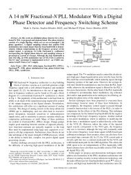
electrostatically driven micro-hydraulic actuator arrays
electrostatically driven micro-hydraulic actuator arrays
electrostatically driven micro-hydraulic actuator arrays

Create successful ePaper yourself
Turn your PDF publications into a flip-book with our unique Google optimized e-Paper software.
into the opposite chamber, causing its membrane to<br />
be deflected out of plane.<br />
By varying the area of the front and back side<br />
chambers, amplification of either force or<br />
displacement is achievable. Furthermore, by carefully<br />
choosing the <strong>hydraulic</strong> liquid we can take advantage<br />
of its high dielectric constant to increase the<br />
electrostatic force (capacitance).<br />
In previously published piston <strong>arrays</strong>, cross talk is<br />
inevitable due to use of a single large actuating<br />
chamber on one side of the wafer for actuating all of<br />
the cells in an array on the opposite side of the wafer,<br />
where the small membranes were latched whenever<br />
they were supposed to be at rest [1]. In that design,<br />
the single chamber provides fluidic connections<br />
between the cells during operation, causing crosstalk.<br />
In the new design presented here, each cell is<br />
actuated by its own membrane, minimizing cross talk<br />
between adjacent cells and eliminating the<br />
previously-required dual-side control electrodes. In<br />
addition, the wafer-level fabrication process and shift<br />
from piezoelectric to electrostatic actuation makes<br />
this architecture applicable to a variety of platforms.<br />
For example, external pneumatic devices are widely<br />
used in fluidic devices, since they can provide high<br />
force and large displacement. The EMA design<br />
shown here can provide almost the same<br />
performance, but additionally can be integrated with<br />
other MEMS devices such as <strong>micro</strong>-fluidics on a<br />
single wafer if the proper sequence of fabrication<br />
steps is chosen.<br />
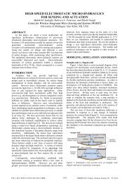
FABRICATION PROCESS<br />
The fabrication process is based on a wafer level<br />
technique for bubble-free encapsulation of a liquid<br />
dielectric that provides the option of having<br />
individual actuated chambers for each of the cells.<br />
The chosen liquid dielectric material is<br />
polytrimethylsiloxane (Silicone oil 1,3,5-trimethyl-<br />
1,1,3,5,5-pentaphenyltrisiloxane) which has a vapor<br />
pressure at room temperature of under 1 mTorr, so<br />
that it can survive the low vacuum inside the<br />
Parylene deposition system [3]. After the oil is<br />
dispensed onto the wafer in the designated locations,<br />
the wafer is loaded in the Parylene deposition tool,<br />
and Parylene is deposited. The polymer conformally<br />
coats the oil on both sides of the wafer, encapsulating<br />
it [3]. Note that almost no leakage or evaporation of<br />
the liquid dielectric is expected during <strong>micro</strong>-system<br />
use since the silicone oil does not evaporate at<br />
atmospheric pressure and room temperature.<br />
Figure 2: Fabrication process.<br />
The fabrication process is shown in Figure 2. It<br />
begins with 3-4 μm dry etching of silicon to form a<br />
recess. This shallow recess plays an important role<br />
during liquid dispensing, as described later. Cr/Au<br />
electrodes are then deposited and patterned. Next,<br />
Cytop TM , an amorphous fluorocarbon polymer that is<br />
transparent and has low gas permeability, is spun,<br />
cured and then patterned with oxygen plasma on both<br />
sides. This hydrophobic layer of Cytop TM repels<br />
silicone oil. As a result, when the oil is later<br />
dispersed, it will be contained within the patterned<br />
Cytop TM -free areas. These areas, which are covered<br />
with oil and then Parylene, will define the chambers<br />
and actuating membranes. After Cytop TM deposition<br />
and patterning, a wafer-through DRIE step connects<br />
the front and backside chambers. The silicone liquid<br />
is then dispensed and is kept in place on the wafer’s<br />
surface by the Cytop TM layer. Although the etchedthrough<br />
channels connect the two sides of the wafer,<br />
the surface tension at the bottom side, resulting from<br />
the effective contact angle modification at the edge of<br />
the shallow trench, prevents the liquid from flowing<br />
out and provides a way to obtain different initial<br />
shapes of the Parylene membranes on the top and<br />
bottom sides.<br />
In a single Parylene deposition run, the dielectric<br />
liquid is encapsulated on both sides. The Parylene<br />
deposition is done while the wafer is flipped over in<br />
the deposition chamber, so that the back side faces<br />
up. Figure 3 shows the top and bottom view of one of<br />
the <strong>actuator</strong>s <strong>arrays</strong> made using this technique after<br />
Parylene deposition over the dispensed liquid. This<br />
encapsulation is bubble free since the deposition of<br />
16
![[Sample B: Approval/Signature Sheet]](https://img.yumpu.com/34084789/1/190x245/sample-b-approval-signature-sheet.jpg?quality=85)