A 14 mW Fractional-N PLL Modulator With a Digital ... - IEEE Xplore
A 14 mW Fractional-N PLL Modulator With a Digital ... - IEEE Xplore
A 14 mW Fractional-N PLL Modulator With a Digital ... - IEEE Xplore

Create successful ePaper yourself
Turn your PDF publications into a flip-book with our unique Google optimized e-Paper software.
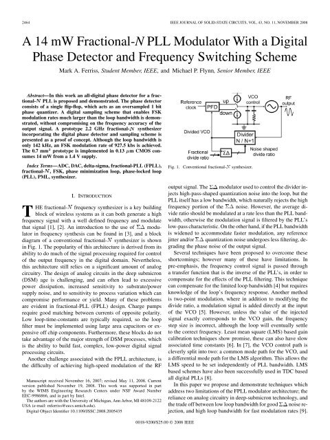
2464 <strong>IEEE</strong> JOURNAL OF SOLID-STATE CIRCUITS, VOL. 43, NO. 11, NOVEMBER 2008<br />
A <strong>14</strong> <strong>mW</strong> <strong>Fractional</strong>-N <strong>PLL</strong> <strong>Modulator</strong> <strong>With</strong> a <strong>Digital</strong><br />
Phase Detector and Frequency Switching Scheme<br />
Mark A. Ferriss, Student Member, <strong>IEEE</strong>, and Michael P. Flynn, Senior Member, <strong>IEEE</strong><br />
Abstract—In this work an all-digital phase detector for a fractional-<br />
<strong>PLL</strong> is proposed and demonstrated. The phase detector<br />
consists of a single flip-flop, which acts as an oversampled 1 bit<br />
phase quantizer. A digital sampling scheme that enables FSK<br />
modulation rates much larger than the loop bandwidth is demonstrated,<br />
without compromising on the frequency accuracy of the<br />
output signal. A prototype 2.2 GHz fractional- synthesizer<br />
incorporating the digital phase detector and sampling scheme is<br />
presented as a proof of concept. Although the loop bandwidth is<br />
only <strong>14</strong>2 kHz, an FSK modulation rate of 927.5 kbs is achieved.<br />
The 0.7 mm 2 prototype is implemented in 0.13 m CMOS consumes<br />
<strong>14</strong> <strong>mW</strong> from a 1.4 V supply.<br />
Index Terms—ADC, DAC, delta-sigma, fractional-<strong>PLL</strong> (F<strong>PLL</strong>),<br />
fractional- , FSK, phase minimization loop, phase-locked loop<br />
(<strong>PLL</strong>), PML, synthesizer.<br />
I. INTRODUCTION<br />
T<br />
HE fractional- frequency synthesizer is a key building<br />
block of wireless systems as it can both generate a high<br />
frequency signal with a well defined frequency and modulate<br />
that signal [1], [2]. An introduction to the use of modulator<br />
in frequency synthesis can be found in [3], and a block<br />
diagram of a conventional fractional- synthesizer is shown<br />
in Fig. 1. The popularity of this architecture is derived from its<br />
ability to do much of the signal processing required for control<br />
of the output frequency in the digital domain. Nevertheless,<br />
this architecture still relies on a significant amount of analog<br />
circuitry. The design of analog circuits in the deep submicron<br />
(DSM) age is challenging, and can often lead to excessive<br />
power dissipation, increased sensitivity to substrate/power<br />
supply noise, and to sensitivity to process variation which can<br />
compromise performance or yield. Many of these problems<br />
are evident in fractional-<strong>PLL</strong> (F<strong>PLL</strong>) design. Charge pumps<br />
require good matching between currents of opposite polarity.<br />
Low loop-time-constants are typically required, so the loop<br />
filter must be implemented using large area capacitors or expensive<br />
off chip components. Furthermore, these blocks do not<br />
take advantage of the major strength of DSM processes, which<br />
is the ability to build fast, complex, low-power digital signal<br />
processing circuits.<br />
Another challenge associated with the F<strong>PLL</strong> architecture, is<br />
the difficulty of achieving high-speed modulation of the RF<br />
Manuscript received November 16, 2007; revised May 11, 2008. Current<br />
version published November 19, 2008. This work was supported in part<br />
by the WIMS Engineering Research Centers under NSF Award Number<br />
EEC-9986866, and in part by Intel.<br />
The authors are with the University of Michigan, Ann Arbor, MI 48109-2122<br />
USA (e-mail: mferriss@eecs.umich.edu).<br />
<strong>Digital</strong> Object Identifier 10.1109/JSSC.2008.2005435<br />
Fig. 1. Conventional fractional-N synthesizer.<br />
output signal. The modulator used to control the divider injects<br />
high-pass-shaped quantization noise into the loop, but the<br />
<strong>PLL</strong> itself has a low bandwidth, which naturally rejects the high<br />
frequency portion of the noise. However, the average divide<br />
ratio should be modulated at a rate less than the <strong>PLL</strong> bandwidth,<br />
otherwise the modulation signal is filtered by the <strong>PLL</strong>’s<br />
low-pass characteristic. On the other hand, if the <strong>PLL</strong> bandwidth<br />
is widened to accommodate faster modulation, any reference<br />
jitter and/or quantization noise undergoes less filtering, degrading<br />
the phase noise of the output signal.<br />
Several techniques have been proposed to overcome these<br />
shortcomings; however many of these have limitations. In<br />
pre-emphasis, the frequency control signal is passed through<br />
a transfer function that is the inverse of the <strong>PLL</strong>’s, in order to<br />
compensate for the effects of the <strong>PLL</strong> filtering. This technique<br />
can compensate for the limited loop bandwidth [4] but requires<br />
knowledge of the loop’s frequency response. Another method<br />
is two-point modulation, where in addition to modifying the<br />
divide ratio, a modulation signal is added directly at the input<br />
of the VCO [5]. However, unless the value of the injected<br />
signal exactly corresponds to the VCO gain, the frequency<br />
step size is incorrect, although the loop will eventually settle<br />
to the correct frequency. Least mean square (LMS) based gain<br />
calibration techniques show promise, these can also have slow<br />
associated time constants [6]. In [7], the VCO control path is<br />
cleverly split into two: a common mode path for the VCO, and<br />
a differential mode path for the LMS algorithm. This allows the<br />
LMS speed to be set independently of <strong>PLL</strong> bandwidth. LMS<br />
based schemes have also been successfully used in TDC based<br />
all digital <strong>PLL</strong>s [8].<br />
In this paper we propose and demonstrate techniques which<br />
address two limitations of the F<strong>PLL</strong> modulator architecture; the<br />
reliance on analog circuitry in deep-submicron technology, and<br />
the trade off between low loop bandwidth for good noise rejection,<br />
and high loop bandwidth for fast modulation rates [9].<br />
0018-9200/$25.00 © 2008 <strong>IEEE</strong>
FERRISS AND FLYNN: A <strong>14</strong> <strong>mW</strong> FRACTIONAL-N <strong>PLL</strong> MODULATOR WITH A DIGITAL PHASE DETECTOR AND FREQUENCY SWITCHING SCHEME 2465<br />
Section II introduces an all-digital phase detector, which relies<br />
on a single flip-flop for phase quantization. Section III introduces<br />
a simple digital dual-modulation scheme that alleviates<br />
the tradeoff between loop bandwidth and switching speed, for<br />
FSK modulation schemes. Section IV discusses additional implementation<br />
details, and finally Section V discusses measured<br />
results and conclusions.<br />
Fig. 2. Using a flip-flop as a phase quantizer.<br />
II. DIGITAL PHASE DETECTOR<br />
An F<strong>PLL</strong> system can be considered to be a type of digital-to-analog<br />
or more specifically a digital-to-frequency<br />
converter, with the phase of the input clock acting as the reference,<br />
the frequency of the input clock corresponding to the<br />
sampling rate, the divider control corresponding to the digital<br />
input, and finally the frequency of the RF signal corresponds<br />
to the output. It should come as no surprise that many of the<br />
challenges associated with building these systems in deep sub<br />
micron (DSM) processes are similar to the challenges associated<br />
with ADC/DAC design. In this work we employ converter<br />
design techniques in order overcome some of these limitations.<br />
A block diagram of a conventional fractional- synthesizer<br />
can be seen in Fig. 1. The information extracted by<br />
the phase detector is inherently analog in nature, since the<br />
phase information is not synchronized to either the reference<br />
clock or the divided down VCO clock, and is not quantized.<br />
Although conventional XOR and tristate phase detectors utilize<br />
digital building blocks, a charge pump and filter are still<br />
required to extract useful phase-difference information. In [11]<br />
a time-to-digital converter (TDC) uses multiple flip-flops and<br />
unit delays (in practice inverters) to quantize the time difference<br />
between the edges of the reference clock and feedback clock.<br />
<strong>With</strong> this approach, resolution and linearity are dependant on<br />
the speed and matching of the unit delay elements, and hence<br />
inherently process dependant.<br />
If a conventional TDC is analogous to a flash ADC, with<br />
the unit delays setting the quantization steps, then the proposed<br />
phase detector is analogous to an oversampling ADC, with oversampling<br />
and a phase integration loop used to improve the performance<br />
of a coarse single-bit phase quantizer. To achieve this<br />
we utilize a unique property of a fractional- <strong>PLL</strong>, that is the<br />
ability to control the frequency of the signal coming from the<br />
programmable divider by changing the divide ratio.<br />
The proposed phase detection technique uses a single flip-flop<br />
as a phase comparator, while an additional negative feedback<br />
loop around the programmable divider keeps the phases of the<br />
two clocks aligned to within a single quantization step. On the<br />
rising edge of the reference clock, the flip-flop samples the divided-down<br />
VCO signal, determining whether the divided clock<br />
is ahead or behind the reference clock. In this way, the flip-flop<br />
effectively acts as a one-bit phase quantizer. In Fig. 2 a single<br />
flip-flop is used to quantize the phase difference, , between<br />
the reference clock and the divided down VCO clock. The quantization<br />
noise of the controlled divider is added to the divided<br />
down VCO clock and this acts as dither for the phase<br />
quantizer. If this dither were absent, and for example if is<br />
positive, then the output of the flip-flip (quantizer) would always<br />
be one, irrespective of the magnitude of phase difference<br />
between the divided down clock and reference clock. In the<br />
Fig. 3. New phase detector configuration with the phase minimization loop<br />
(PML).<br />
presence of the dither, the output of the flip-flop is sometimes<br />
one and sometimes zero. Similar to an oversampled ADC, the<br />
low-pass-filtered output of the flip-flop is proportional to .<br />
An approximately linear relationship is achieved if the phase<br />
difference can be kept small relative to magnitude of dither.<br />
Single bit quantized phase detectors can also be found in<br />
Bang-Bang <strong>PLL</strong>s. In a Bang-Bang <strong>PLL</strong> the output signal typically<br />
goes directly to the phase detector (or through a static divider),<br />
hence the phase of the <strong>PLL</strong> output or <strong>PLL</strong> input signal<br />
must change if the output of the phase quantizer is to change<br />
[10]. Therefore in a Bang-Bang <strong>PLL</strong>, the phase quantizer can<br />
only provide information on the polarity of any phase difference<br />
between the system input and output. In contrast, in this work<br />
the VCO output passes through a controlled programmable<br />
divider before it reaches the phase-detector. This means that by<br />
changing the divide value, the phase quantizer is exercised in<br />
the absence of any change in excess phase of the VCO output.<br />
The also provide dither to the phase quantizer, an important<br />
requirement for any oversampled quantizer.<br />
An additional inner feedback loop, seen in Fig. 3, is introduced<br />
to keep the phase difference between the two clocks<br />
small, i.e., minimizing . For this reason the new loop is<br />
called the phase minimization loop (PML). This phase feedback<br />
scheme might be recognized as being similar in form to<br />
a delta modulator, a commonly used ADC/DAC architecture.<br />
In a delta modulator the forward path consists of a quantizer,<br />
and the feedback path includes an integrator. (In this work the<br />
integration occurs because phase information is fedback to the<br />
frequency control of the divider.) The integrator keeps the phase<br />
difference at the input of the quantizer small. Although the<br />
overall <strong>PLL</strong> keeps the average of at zero, the instantaneous<br />
value of is a function of the bandwidth of the <strong>PLL</strong>, which<br />
cannot be set arbitrarily large. The bandwidth of the inner loop,<br />
however, can be set to be larger than that of the overall <strong>PLL</strong>,<br />
hence can do a better job keeping the two clocks in close phase<br />
alignment. This is necessary in order for the phase detector<br />
to behave in an approximately linear fashion. If the phase
2466 <strong>IEEE</strong> JOURNAL OF SOLID-STATE CIRCUITS, VOL. 43, NO. 11, NOVEMBER 2008<br />
Fig. 4. Small-signal model of the divider.<br />
deviation, , is too large then the quantizer output becomes<br />
stuck at 1 or , and the dither will not have the desired effect.<br />
The one-bit output of the flip-flop is passed through a linear<br />
scaling block , so that the output of the quantizer is .<br />
is used to set the quantizer step size. A similar technique<br />
is presented as part of a frequency discriminator 1 in [13], which<br />
can be used as an RF demodulator or as part of a <strong>Fractional</strong>-<br />
<strong>PLL</strong> [<strong>14</strong>], [15] 2 , in which the quantized phase signal is fed<br />
directly back to the divider control, and there is no in the<br />
feedback path.<br />
The only pseudo-analog component is the decision making<br />
flip-flop, while everything else is synchronous digital circuitry.<br />
The flip-flop should be treated in a similar fashion to a comparator<br />
in an ADC, as its set-up and hold times are not necessarily<br />
respected, as would be the case in a truly digital system.<br />
Therefore attention must be paid to meta-stability, gain, and<br />
other characteristics as for a comparator in an ADC. Some techniques<br />
to build a suitable flip-flop are discussed in [11]. However,<br />
for our design a flip-flop from a standard cell library is<br />
adequate. This digital approach does not rely on component<br />
matching or on any process dependant parameters such as inverter<br />
delays.<br />
From a phase perspective, the PML incorporates an integrator<br />
in its feedback path. This is because the quantized phase information<br />
is fed back to the frequency control of the divider. As<br />
phase is the integral of frequency, this implies the presence of<br />
an integrator in the phase domain. Referring again to Fig. 3, the<br />
presence of this integrator changes nature of the transfer function<br />
from the VCO output ( ) to the output of the quantization<br />
flip-flop, and also changes the transfer function from the<br />
modulator input to the output of the flip-flop. A small-signal<br />
phase-domain model of the divider is shown in Fig. 4, the derivation<br />
of which is discussed in [12]. The phase transfer function<br />
from the VCO output to the output of the flip-flop is now<br />
high-pass instead of all-pass, because of the integrator in the<br />
feedback path. As shown in Fig. 3, a digital integrator placed<br />
at the output of the quantizer compensates for the change in<br />
transfer function that the PML has caused.<br />
Fig. 5 shows an overview of the architecture with the proposed<br />
phase detector configuration. The output of the integrator<br />
goes to a DAC, which drives the analog control of the VCO, so<br />
as to complete the loop. is a digital gain that modifies the<br />
1 In this work Phase Minimization Loop is preferred to Frequency Discriminator,<br />
as the feedback is used to minimize the phase difference at the input of<br />
the quantizer.<br />
2 Also [13]–[15] include analog integrators with charge pumps in order to implement<br />
higher order noise shaping of the frequency error, a step that has been<br />
avoided in this work in order to maximize the digital nature of the system.<br />
Fig. 5. Overall architecture for proposed F<strong>PLL</strong>.<br />
bandwidth of the outer loop, while gain block<br />
bandwidth of the inner loop.<br />
modifies the<br />
A. Small-Signal Model<br />
A small-signal model of the overall system is required in<br />
order to calculate the loop dynamics, and to predict the phase<br />
noise at the output. The overall approach for calculating phase<br />
noise is based on [12]. The general strategy is to begin with a<br />
linear model for each of the components. Using this, the closedloop<br />
transfer function for the overall loop , is calculated.<br />
Next, the transfer function between each noise source and the<br />
<strong>PLL</strong> output is calculated using . In this way the phase noise<br />
at the output can be calculated in a straightforward manner. This<br />
is a linear analysis, and nonlinear effects within the loop are not<br />
considered.<br />
The overall small-signal model for the system is shown in<br />
Fig. 6. The loops are labeled and . The<br />
term models an RC filter at the output of the DACs which<br />
filters the DAC’s quantization noise. The overall model<br />
contains a mixture of discrete and continuous-time transfer<br />
functions and noise sources. The term is a fitting parameter<br />
that models the phase detector gain, as measured in<br />
simulation experiments. is the nominal division ratio,<br />
is the VCO gain, and , are digital constants.<br />
The noise sources which are shown here are the phase detector<br />
quantizer noise ( ), the DAC noise ( ),<br />
the VCO phase noise ( ), and the divider noise<br />
( ). In Fig. 6, sampling is denoted by the transfer<br />
function, while the DAC is represented by the block. This is<br />
because of the frequency domain relationship between a continuous<br />
time signal and its sampled equivalent, as described by<br />
. Deriving the loop transfer<br />
functions and the noise at the output involves approximating<br />
discrete noise sources as continuous ones, in a similar way to<br />
[12]. The analog transfer function for the PML is expressed in<br />
(1), where is the open-loop gain:<br />
If the digital integrators are approximated as continuous time<br />
integrators of value then the open-loop gain can be<br />
given by<br />
(1)<br />
(2)
FERRISS AND FLYNN: A <strong>14</strong> <strong>mW</strong> FRACTIONAL-N <strong>PLL</strong> MODULATOR WITH A DIGITAL PHASE DETECTOR AND FREQUENCY SWITCHING SCHEME 2467<br />
Fig. 6. Small-signal phase domain model will noise sources.<br />
Fig. 7. (a) Simplified model for inner loop. (b) Simplified model for both loops.<br />
Similarly, for the output loop, , the closed-loop and<br />
open-loop responses are given in (3) and (4), respectively:<br />
(3)<br />
If the higher order poles, , are ignored, then we can<br />
combine (1),(2),(3) and (4) to give the overall closed-loop response<br />
(5):<br />
(4)<br />
(5)<br />
We note that this is an all pole system; there are no zeros.<br />
(Dual loop architectures have also been used in fiber optic communication<br />
<strong>PLL</strong>s to implement transfer function with no zeros<br />
[16].)<br />
In Fig. 7(a) the loop is redrawn with the inner loop, ,<br />
replaced with its equivalent transfer function. Here the only inputs<br />
considered are the reference, the frequency control word<br />
and noise. In Fig. 7(b) the outer loop, , is also replaced.<br />
From this it is straightforward to deduce the transfer<br />
functions from input to output. The relationship between the<br />
reference phase and output phase is given in (6). ( is first<br />
multiplied by , to convert it to an approximate equivalent continuous<br />
time source.)<br />
(6)<br />
Fig. 8. Plot of measured and calculated noise sources.<br />
In a similar manner, the transfer function for all of the noise<br />
sources can be calculated. The various noise sources, and the<br />
total calculated noise, and measured noise are plotted in Fig. 8.<br />
For low and very high frequencies the phase noise is dominated<br />
by the VCO noise, while for frequencies close to the loop bandwidth<br />
(<strong>14</strong>2 kHz) the phase detector quantization noise (PD noise<br />
in Fig. 8) is significant. The poor VCO phase noise performance<br />
is due in part to the low quality factor of available integrated inductors<br />
on this process. The divider noise does not make a<br />
significant contribution to the output phase noise. This is because<br />
the reference clock used is large in comparison to the<br />
loop bandwidth, and hence most of the quantization noise<br />
is shaped to outside of the <strong>PLL</strong> loop bandwidth.<br />
Both of the two <strong>PLL</strong> loops contain a single net integrator, and<br />
therefore each loop is a Type 1 loop. This may seem surprising
2468 <strong>IEEE</strong> JOURNAL OF SOLID-STATE CIRCUITS, VOL. 43, NO. 11, NOVEMBER 2008<br />
Fig. 9. (a) Simplified <strong>PLL</strong>. Input to VCO is analogous to the output frequency.<br />
(b) Plot of required output versus actual output.<br />
considering that the small-signal diagram of Fig. 6 appears to<br />
incorporate two integrators in the outer loop ( ); the VCO<br />
and the digital integrator at the output of the phase quantizer.<br />
However as already mentioned, the digital integrator cancels the<br />
zero introduced by the PML, leaving a net single DC pole.<br />
Fig. 10.<br />
(a) <strong>PLL</strong> with Delta added. (b) Simulation VCO input.<br />
III. SAMPLING SCHEME<br />
The wide fractional- <strong>PLL</strong> loop-bandwidth required for<br />
high-speed modulation, conflicts with the low loop bandwidth<br />
favored for suppression of noise, phase detector noise,<br />
and reference jitter. In this section, a new technique which<br />
breaks the link between loop-bandwidth and the modulation<br />
rate for frequency-shift-keying schemes is presented. In a<br />
standard F<strong>PLL</strong>, the output frequency is modified by changing<br />
the division ratio control, eventually leading to a change in the<br />
VCO control voltage. If the exact VCO gain were known, then<br />
in addition to changing the division ratio control, a signal could<br />
be injected directly into the input of the VCO, as in two point<br />
modulation. In the proposed scheme, knowledge of the exact<br />
VCO gain is not required. Instead, using some simple signal<br />
processing, the required step size at the input of VCO is learned<br />
from previous changes in VCO control in response to changes<br />
in the modulator input. 3<br />
Consider the case where the loop is to switch between two<br />
output different frequencies, and , such as for 2-FSK, and<br />
assume that the loop frequency is initially settled at the average<br />
of and . If the bandwidth of the loop is not large enough<br />
in a standard F<strong>PLL</strong> then the frequency never settles correctly<br />
to or [Fig. 9(b)]. In Fig. 9(a) a simplified version of the<br />
<strong>PLL</strong> is shown. The input to the VCO can be considered to be<br />
analogous to the frequency of the output signal, and it follows<br />
that if the output frequency is to switch instantaneously then<br />
the input to VCO must also switch instantaneously. In the proposed<br />
scheme at the end of each data-bit period the digital value<br />
that determines the VCO input is sampled. When switching between<br />
the two desired frequencies, and , the most recently<br />
sampled values are subtracted from each other. The result of this<br />
subtraction [“Delta” in Fig. 10(a)] is added to the VCO control<br />
3 In summary, this is a form of two point modulation with a simple calibration<br />
scheme.<br />
Fig. 11.<br />
Details of the sampling scheme.<br />
for frequency , to give an initial digital VCO control value for<br />
frequency . As the required frequency continues to switch between<br />
frequencies and , then the sampled value of Delta<br />
converges on the correct VCO input difference for the required<br />
frequencies and . In other words, the sampling scheme iteratively<br />
learns the required step size Delta. Fig. 10(b) shows the<br />
output frequency, using the sampling scheme. As can be seen,<br />
after a few iterations Delta reaches the correct step size, and the<br />
frequency is able to switch instantaneously. The loop bandwidth<br />
determines how quickly Delta reaches its final value, but does<br />
not affect the switching frequency. This does not presuppose<br />
any knowledge of the analog characteristics of the loop, aside<br />
from monotonic behavior. For example if the VCO gain were<br />
to change due supply or temperature changes then the value of<br />
Delta would be quickly updated. This scheme does not update<br />
every reference period; Delta is only updated on the edges of<br />
the data to be transmitted. A disadvantage of this approach is<br />
its lack of generality; that is it can only be used for modulation<br />
schemes which are limited to a small set of discrete frequencies,<br />
such as unfiltered 2-FSK.<br />
A more detailed block diagram of the sampling scheme is<br />
shown in Fig. 11. The control path for the VCO is split into two<br />
paths, one path for each of the two frequencies and . Each<br />
path contains a DAC, the output of which goes to an analog<br />
multiplexer. The two DAC control signals are sampled when<br />
the transmission data transitions from zero to one and from one<br />
to zero, which corresponds to the switching instants from frequency<br />
to and from frequency to , respectively. The<br />
difference, Delta, is then added to the signal from the phase<br />
detector. Multiplexing between the two DACs is done in the
FERRISS AND FLYNN: A <strong>14</strong> <strong>mW</strong> FRACTIONAL-N <strong>PLL</strong> MODULATOR WITH A DIGITAL PHASE DETECTOR AND FREQUENCY SWITCHING SCHEME 2469<br />
Fig. 12. Complete architecture.<br />
Fig. 13. Overview of analog section.<br />
analog domain after the reconstruction filters. The filters contain<br />
two higher order RC poles to filter the DAC noise. As<br />
the input to the VCO is required to change instantaneously, the<br />
multiplexer must be placed after these poles.<br />
The complete architecture including the digital phase detector<br />
and the new sampling scheme is shown in Fig. 12. The<br />
frequency switching method allows fast frequency modulation<br />
within a low loop bandwidth, as the frequency switching is<br />
not limited by the bandwidth of the loop, provided that the<br />
loop needs only to switch between a small number of discrete<br />
frequencies. This also demonstrates the usefulness of having all<br />
the relevant signals in the digital domain. An analog equivalent<br />
of the above scheme is possible in principle, however implementing<br />
the samplers, adders and subtractors as analog circuits<br />
would introduce debilitating additional complexity.<br />
IV. IMPLEMENTATION DETAILS<br />
A reference clock of 185.5 MHz is used, with a nominal<br />
output frequency 2.24 GHz, which corresponds to a nominal<br />
division ratio of . was set to 0.01, and<br />
the loop gain ( ) is set at 0.025, resulting in a loop bandwidth<br />
of <strong>14</strong>2 kHz. The PML loop has an estimated bandwidth<br />
of 1.2 MHz. The VCO analog gain is 25 MHz/V, and an additional<br />
500 MHz tuning range is achieved using digital switches<br />
which add or remove VCO capacitance. From simulation experiments,<br />
the acquisition range was determined to be approximately<br />
150 MHz, which is significantly larger that the VCO<br />
tuning range, and so no additional acquisition aids were implemented.<br />
The analog tuning range is deliberately made small in<br />
order to prevent DAC quantization noise from excessively contributing<br />
to the output phase noise. A relatively high reference<br />
frequency is required, so that the phase quantizer is adequately<br />
oversampled. Each doubling of the oversampling rate leads to a<br />
3 dB reduction in in-band quantization noise.<br />
In order to convert from the digital to the analog domain, a<br />
first order controls a simple 5 bit string DAC. If a higher<br />
frequency reference clock or a DAC quantizer with more bits<br />
is used, then the VCO analog tuning range can be increased<br />
without degrading output phase noise. An alterative approach<br />
would be to implement a fully digitally controlled oscillator,<br />
such as presented in [17]. The programmable divider is based<br />
on the modular architecture presented in [18], where each of<br />
Fig. <strong>14</strong>.<br />
Output buffer.<br />
the 2/3 divider cells is identical. The divider division ratio can<br />
be set from 8 to 15. An overview of the DAC and VCO is shown<br />
in Fig. 13. Each DAC draws 1.4 mA from the 1.4 V supply, and<br />
the VCO draws approximately 2 mA. The digital auto-route,<br />
which includes all of digital except the divider, consumes approximately<br />
6 <strong>mW</strong>.<br />
The design of even simple output buffers in very low headroom<br />
processes is not trivial. If a source follower were used, then<br />
enough headroom would be required for both the signal swing<br />
and the of the MOS devices. In this work a simple output<br />
buffer is used, which requires little headroom, and sets the DC<br />
value of the output node automatically, without requiring complex<br />
common mode feedback circuitry. The buffer is shown in<br />
Fig. <strong>14</strong>. At DC, the buffer acts a current source driving current<br />
into a diode connected load. In this way the DC point of the<br />
output will be approximately<br />
, which will be<br />
close to for this process. On the other hand, at high frequencies,<br />
the buffer acts as a push-pull amplifier. The DC values<br />
at the input and output of the buffer are not important, as both<br />
input and output are ac coupled.<br />
The prototype transmitter is implemented in 0.13 m mixedmode<br />
CMOS and occupies an active area of 0.7 mm , and a<br />
total area of 2 mm including pads. The layout of the prototype<br />
is shown in Fig. 15. It is worth noting that even though many<br />
of the analog components have been removed, the area is still<br />
dominated by the area of the remaining analog blocks. The digital<br />
auto-routed logic takes up 0.075 mm , a small fraction of<br />
the overall area, despite dominating the architecture shown in
2470 <strong>IEEE</strong> JOURNAL OF SOLID-STATE CIRCUITS, VOL. 43, NO. 11, NOVEMBER 2008<br />
Fig. 15. Micrograph.<br />
Fig. 17.<br />
Trellis diagram of phase output.<br />
equivalents. In addition, a new technique has been developed<br />
which allows for frequency modulation at a rate significantly<br />
faster rate than the loop bandwidth. As transistor gate length<br />
continues to scale down, design of analog circuitry will become<br />
even more challenging, while the area and power costs of digital<br />
circuits continues to decrease. Techniques such as the ones presented<br />
here will become crucial in order to move from analog<br />
dominated circuitry to digital circuitry.<br />
Fig. 16. Modulation spectrum.<br />
Fig. 12. This demonstrates the area savings that can be achieved<br />
by going from an analog dominated architecture to a digital<br />
dominated architecture.<br />
V. RESULTS AND CONCLUSION<br />
The prototype consumes <strong>14</strong> <strong>mW</strong> from a 1.4 V supply. Fig. 16<br />
shows the measured output spectrums for a pure synthesized<br />
tone and for random data with an FSK data modulation rate of<br />
927.5 kbits/s. Fig. 8 shows the measured phase noise.<br />
The VCO was originally intended to operate in the 2.4 GHz<br />
ISM band. However, due to process variation, the maximum<br />
VCO frequency was 2.24 GHz, even considering the digital<br />
tuning capacitors. Fig. 17 shows a trellis diagram of the measured<br />
output phase. In this measurement various random data<br />
patterns are applied to the F<strong>PLL</strong>, and the corresponding phase<br />
change at the output is measured, and overlaid. As can be seen,<br />
the phase changes direction instantaneously, which is the equivalent<br />
to the frequency changing instantaneously. Even with a<br />
loop bandwidth of <strong>14</strong>2 kHz, a data rate of 927.5 kb/s is still possible.<br />
<strong>With</strong>out the new switching scheme the data rate would be<br />
restricted to a fraction of the loop bandwidth.<br />
In this work, two techniques are proposed and demonstrated.<br />
First, a digital phase detector allows a significant portion of the<br />
analog circuitry required in a F<strong>PLL</strong> to be replaced with digital<br />
ACKNOWLEDGMENT<br />
The authors acknowledge the support of Intel. They would<br />
also like to thank all of the people who provided invaluable<br />
advice and support throughout this project, including J. Kang,<br />
J.-Y. Chen, M. Mansuri, S. Naraghi, J. Pernillo, I. Bogue, D. Shi,<br />
F. Kocer, and C. Conroy. Architectural investigation was aided<br />
by CppSim [19]. The authors also thank the reviewers for invaluable<br />
insights and suggestions.<br />
REFERENCES<br />
[1] T. A. Riley, M. A. Copeland, and T. A. Kwasniewski, “Delta-sigma<br />
modulation in fractional-N frequency synthesis,” <strong>IEEE</strong> J. Solid-State<br />
Circuits, vol. 28, no. 5, pp. 553–559, May 1993.<br />
[2] E. Gotz, H. Krobel, G. Marzinger, B. Memmler, C. Munker, B. Neurauter,<br />
D. Romer, J. Rubach, W. Schelmbauer, M. Scholz, M. Simon, U.<br />
Steinacker, and C. Stoger, “A quad-band low power single chip direct<br />
conversion CMOS transceiver with 61-modulation loop for GSM,” in<br />
Proc. Eur. Solid-State Circuits Conf., 2003, pp. 217–220.<br />
[3] I. Galton, “Delta-sigma data conversion in wireless transceivers,” <strong>IEEE</strong><br />
Trans. Theory Tech., vol. 50, no. 1, pp. 302–315, Jan. 2002.<br />
[4] M. H. Perrott, “Techniques for high data rate modulation and low power<br />
operation of fractional-N frequency synthesizers,” Ph.D. dissertation,<br />
Massachusetts Inst. Technol. (MIT), Cambridge, MA, 1997.<br />
[5] R. A. Meyers and P. H. Waters, “Synthesizer review for pan-European<br />
digital cellular radio,” in Proc. <strong>IEEE</strong> VLSI Implementations for Second<br />
Generation <strong>Digital</strong> Cordless and Mobile Telecommunication Systems<br />
Colloq., 1990, pp. 8/1–8/8.<br />
[6] M. Gupta and B. Song, “A 1.8-GHz spur-cancelled fractional-N frequency<br />
synthesizer with LMS-based DAC gain calibration,” <strong>IEEE</strong> J.<br />
Solid-State Circuits, vol. 41, no. 12, pp. 2842–2851, Dec. 2006.<br />
[7] A. Swaminathan, K. Wang, and I. Galton, “A wide-bandwidth 2.4 GHz<br />
ISM band fractional-N <strong>PLL</strong> with adaptive phase noise cancellation,”<br />
<strong>IEEE</strong> J. Solid-State Circuits, vol. 42, no. 12, pp. 2639–2650, Dec. 2007.
FERRISS AND FLYNN: A <strong>14</strong> <strong>mW</strong> FRACTIONAL-N <strong>PLL</strong> MODULATOR WITH A DIGITAL PHASE DETECTOR AND FREQUENCY SWITCHING SCHEME 2471<br />
[8] R. Staszewski, J. Wallberg, C. M. Hung, G. Feygin, M. Entezari, and<br />
D. Leipold, “LMS-based calibration of an RF digitally controlled oscillator<br />
for mobile phones,” <strong>IEEE</strong> Trans. Circuits Syst. II, vol. 53, no.<br />
3, pp. 225–229, Mar. 2006.<br />
[9] M. Ferriss and M. P. Flynn, “A <strong>14</strong> <strong>mW</strong> fractional-N <strong>PLL</strong> modulator<br />
with an enhanced digital phase detector and frequency switching<br />
scheme,” in <strong>IEEE</strong> ISSCC Dig. Tech. Papers, 2007, pp. 353–353.<br />
[10] R. C. Walker, “Designing bang-bang <strong>PLL</strong>s for clock and data recovery<br />
in serial data transmission systems,” in Phase-Locking in High-Performance<br />
Systems. Piscataway, NJ: <strong>IEEE</strong> Press, 2003.<br />
[11] R. Staszewski, S. Vemulapalli, P. Vallur, J. Wallberg, and P. T. Balsara,<br />
“1.3 V 20 ps time-to-digital converter for frequency synthesis in 90-nm<br />
CMOS,” <strong>IEEE</strong> Trans. Circuits Syst. II, vol. 53, no. 3, pp. 220–224, Mar.<br />
2006.<br />
[12] M. H. Perrott and M. D. Trott, “A modeling approach for 6-1 fractional-N<br />
frequency synthesizers allowing straightforward noise analysis,”<br />
<strong>IEEE</strong> J. Solid-State Circuits, vol. 37, no. 8, pp. 1028–1038, Aug.<br />
2002.<br />
[13] R. Beards and M. Copeland, “An oversampling delta-sigma frequency<br />
discriminator,” <strong>IEEE</strong> Trans. Circuits Syst. II, vol. 41, no. 1, pp. 26–32,<br />
Jan. 1994.<br />
[<strong>14</strong>] W. Bax, T. Riley, C. Plett, and M. Copeland, “A 61 frequency discriminator<br />
based synthesizer,” in Proc. Int. Symp. Circuits and Systems<br />
(ISCAS), 1995, pp. 1–4.<br />
[15] W. Bax and M. Copeland, “A GMSK modulator using 61 frequency<br />
discriminator-based synthesizer,” <strong>IEEE</strong> J. Solid-State Circuits, vol. 36,<br />
no. 8, pp. 1218–1227, Aug. 2001.<br />
[16] T. H. Lee and J. F. Bulzacchelli, “A 155-MHz clock recovery delayand<br />
phase-locked loop,” <strong>IEEE</strong> J. Solid-State Circuits, vol. 27, no. 12,<br />
pp. 1736–1746, Dec. 1992.<br />
[17] C. M. Hung, R. B. Staszewski, N. Barton, M. C. Lee, and D. Leipold,<br />
“A digitally controlled oscillator system for SAW-less transmitters<br />
in cellular handsets,” <strong>IEEE</strong> J. Solid-State Circuits, vol. 41, no. 5, pp.<br />
1160–1170, May 2006.<br />
[18] C. S. Vaucher, I. Ferencic, M. Locher, S. Sedvallson, U. Voegeli, and Z.<br />
Wang, “A family of low-power truly modular programmable dividers<br />
in standard 0.35-m CMOS technology,” <strong>IEEE</strong> J. Solid-State Circuits,<br />
vol. 35, no. 7, pp. 1039–1045, Jul. 2000.<br />
[19] M. H. Perrott, CppSim Behavioral Simulator Package. [Online]. Available:<br />
http://www-mtl.mit.edu/researchgroups/perrottgroup/tools.html<br />
Mark A. Ferriss (S’03–M’08) received the B.E. degree<br />
from University College Cork, Ireland, in 1998,<br />
and the M.S.E. and Ph.D. degrees in electrical engineering<br />
from the University of Michigan, Ann Arbor,<br />
in 2005 and 2008, respectively.<br />
From 1998 to 2002, he was with Analog Devices,<br />
Limerick, Ireland, during which time he worked on<br />
a variety of projects including DACs, switches, controllers,<br />
and <strong>PLL</strong>s for fiber-optic communications.<br />
His interests include RF communication circuits<br />
and analog-to-digital interface circuits. He currently<br />
holds a postdoctoral research position at the University of Michigan.<br />
Michael P. Flynn (S’92–M’95–SM’98) was born in<br />
Cork, Ireland. He received the B.E. and M.Eng.Sc.<br />
degrees from the National University of Ireland at<br />
Cork (UCC) in 1988 and 1990, respectively, and the<br />
Ph.D. degree from Carnegie Mellon University, Pittsburgh,<br />
PA, in 1995.<br />
He joined the University of Michigan, Ann Arbor,<br />
in 2001 and is now an Associate Professor. He is<br />
Thrust Leader responsible for Wireless Interfaces<br />
at Michigan’s Wireless Integrated Microsystems<br />
(WIMS) NSF Engineering Research Center. From<br />
1988 to 1991, he was with the National Microelectronics Research Centre,<br />
Cork, Ireland. He joined National Semiconductor in Santa Clara, CA, in<br />
1993, and from 1995 to 1997 he was a Member of Technical Staff at Texas<br />
Instruments, Dallas, TX. From 1997 to 2001, he was Technical Director and<br />
Fellow at Parthus Technologies, Cork, and during the same period he was also<br />
a part-time faculty member at the Department of Microelectronics, National<br />
University of Ireland, Cork. His technical interests are in data conversion,<br />
high-speed serial data links, and RF circuits.<br />
Dr. Flynn was named a Fellow by the Guggenheim Foundation in 2007.<br />
He received the 2005–2006 Outstanding Achievement Award from the Department<br />
of Electrical Engineering and Computer Science at the University<br />
of Michigan, the National Science Foundation Early Career Award in 2004,<br />
and the 1992–1993 <strong>IEEE</strong> Solid-State Circuits Pre-doctoral Fellowship. He<br />
serves as an Associate Editor of the <strong>IEEE</strong> JOURNAL OF SOLID STATE CIRCUITS<br />
and on the Technical Program Committees of the International Solid State<br />
Circuits Conference (ISSCC) and the Asia Solid State Circuits Conference<br />
(A-SSCC). He was Associate Editor of the <strong>IEEE</strong> TRANSACTIONS ON CIRCUITS<br />
AND SYSTEMS II from 2002 to 2004. He is a Senior Member of the <strong>IEEE</strong> and a<br />
member of Sigma Xi.
![[Sample B: Approval/Signature Sheet]](https://img.yumpu.com/34084789/1/190x245/sample-b-approval-signature-sheet.jpg?quality=85)