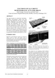
An adaptive write word-line pulse width and voltage modulation ...
An adaptive write word-line pulse width and voltage modulation ...
An adaptive write word-line pulse width and voltage modulation ...

You also want an ePaper? Increase the reach of your titles
YUMPU automatically turns print PDFs into web optimized ePapers that Google loves.
<strong>An</strong> Adaptive Write Word-Line Pulse Width <strong>and</strong> Voltage<br />
Modulation Architecture for Bit-Interleaved 8T SRAMs<br />
Daeyeon Kim 1, 3 , Vikas Ch<strong>and</strong>ra 2 , Robert Aitken 2 , David Blaauw 1 , Dennis Sylvester 1<br />
1 University of Michigan, <strong>An</strong>n Arbor, MI<br />
2 ARM Inc., San Jose, CA<br />
3 Currently with Intel Corporation, Hillsboro, OR<br />
daeyeonk@umich.edu, {vikas.ch<strong>and</strong>ra, rob.aitken}@arm.com, {blaauw, dmcs} @umich.edu<br />
ABSTRACT<br />
We propose an <strong>adaptive</strong> WWL <strong>pulse</strong> <strong>width</strong> <strong>and</strong> <strong>voltage</strong><br />
<strong>modulation</strong> architecture for low <strong>voltage</strong> bit-interleaved 8T<br />
SRAMs. The 8T bitcell offers improved read/<strong>write</strong> margins but<br />
suffers from <strong>write</strong> <strong>and</strong> half select concerns when bit-interleaved<br />
[1]. Also, low <strong>voltage</strong> operation leads to a long-tailed <strong>write</strong> time<br />
distribution, requiring large timing margins <strong>and</strong> limiting V min . To<br />
minimize timing margins <strong>and</strong> reduce V min , both WWL <strong>pulse</strong><br />
<strong>width</strong> <strong>and</strong> <strong>voltage</strong> level are <strong>adaptive</strong>ly modulated by monitoring<br />
written values through the read path. In a 65nm CMOS prototype<br />
chip, V min is lowered from 700mV to 500mV using this technique,<br />
providing 2.55× leakage power reduction <strong>and</strong> 2.4× active power<br />
reduction.<br />
Categories <strong>and</strong> Subject Descriptors<br />
B.3.1 [Memory Structures]: Semiconductor Memories – Static<br />
Memory (SRAM); B.7.1 [Integrated Circuits]: Types <strong>and</strong> Design<br />
Styles – Advanced Technologies, Memory Technologies, VLSI<br />
(very large scale integration); B.8.0 [Performance <strong>and</strong><br />
Reliability]: General<br />
Key<strong>word</strong>s<br />
SRAM, Low Voltage Design, Noise Margin<br />
1. INTRODUCTION<br />
Low <strong>voltage</strong> operation is an effective way to reduce power<br />
consumption due to the resulting quadratic power savings.<br />
Variability at low <strong>voltage</strong> is a challenge however, <strong>and</strong> low <strong>voltage</strong><br />
SRAM in particular is vulnerable to variation <strong>and</strong> functional<br />
failures due to the use of minimum feature sizes in a bitcell <strong>and</strong><br />
large SRAM array sizes. The 8T bitcell [2] (Figure 1) improves<br />
low <strong>voltage</strong> operation by allowing separate optimization of read<br />
<strong>and</strong> <strong>write</strong> paths. Bit-interleaving is essential to avoid soft errors,<br />
particularly at low <strong>voltage</strong>s, but induces half select disturb [3] as<br />
the 6T portion of the 8T bitcell is optimized for <strong>write</strong>. Since half<br />
select <strong>and</strong> writability create a double-sided constraint on WWL<br />
<strong>pulse</strong> <strong>width</strong> <strong>and</strong> WWL <strong>voltage</strong>, WWL control is key to reducing<br />
V min <strong>and</strong> maximizing yield for bit-interleaved 8T SRAMs.<br />
Permission to make digital or hard copies of all or part of this work for<br />
personal or classroom use is granted without fee provided that copies are<br />
not made or distributed for profit or commercial advantage <strong>and</strong> that<br />
copies bear this notice <strong>and</strong> the full citation on the first page. To copy<br />
otherwise, or republish, to post on servers or to redistribute to lists,<br />
requires prior specific permission <strong>and</strong>/or a fee.<br />
ISLPED’12, July 30–August 1, 2012, Redondo Beach, California, USA.<br />
Copyright 2012 ACM 978-1-4503-1249-3/12/07...$10.00.<br />
To mitigate the trade-off between <strong>write</strong> <strong>and</strong> half select, this paper<br />
proposes <strong>adaptive</strong> WWL <strong>voltage</strong> <strong>modulation</strong> with regenerative<br />
half selected bit-<strong>line</strong>s. In addition, SRAM bitcells exhibit a wide<br />
<strong>write</strong> time distribution with a long tail at low <strong>voltage</strong> (Figure 2).<br />
Excessive margins are required due to the few bitcells with long<br />
<strong>write</strong> times. To minimize this impact, we propose a multi-cycle<br />
WBL<br />
WWL PUL<br />
AXL<br />
PDL<br />
VDD<br />
VSS<br />
PUR WWL<br />
PDR<br />
AXR<br />
WBLB<br />
RWL<br />
VSS<br />
RBL<br />
Figure 1. The 8-T bitcell schematic is shown. Write <strong>and</strong> read<br />
are separately optimized.<br />
# of Occurence<br />
3000<br />
2500<br />
1000<br />
500<br />
0<br />
2821<br />
2 ~ 2.5<br />
# of Occurence<br />
1007<br />
2.5 ~ 3<br />
50000<br />
40000<br />
30000<br />
20000<br />
10000<br />
0<br />
3 ~ 3.5<br />
0 ~0.5<br />
398<br />
0.5 ~ 1<br />
1 ~ 1.5<br />
3.5 ~ 4<br />
1.5 ~ 2<br />
1.0V<br />
0.65V<br />
2 ~ 2.5<br />
1.0V<br />
0.65V<br />
2.5 ~ 3<br />
3 ~ 3.5<br />
3.5 ~ 4<br />
Normalized Write Time<br />
170<br />
4 ~ 4.5<br />
4.5 ~ 5<br />
Normalized Write Time<br />
4 ~ 4.5<br />
4.5 ~ 5<br />
> 5<br />
55 101<br />
Figure 2. 10K Monte Carlo simulation results of <strong>write</strong> time<br />
distribution at 0.65V <strong>and</strong> 1.0V. The distribution at 0.65V is<br />
wider with a long tail, increasing design margins.<br />
115<br />
> 5<br />
91
<strong>write</strong> operation where the number of cycles is <strong>adaptive</strong>ly<br />
determined via <strong>write</strong> completion detection, similar to the scheme<br />
used in [4]. Overall performance is improved using the multicycle<br />
<strong>write</strong> scheme.<br />
The importance of dynamic <strong>write</strong> stability has been previously<br />
discussed [5]. A replica-based <strong>adaptive</strong> stability enhancement<br />
technique [6] was proposed. While [6] is replica-based, this work<br />
describes an in situ approach (i.e., it uses actual bitcells in the<br />
SRAM array, eliminating mismatch issues). Adaptive WWL<br />
boosting for 8T SRAMs [7] was also proposed but it does not use<br />
a bit-interleaved array <strong>and</strong> hence is susceptible to soft errors. Half<br />
select prevention using a pre-read technique was proposed in [8]<br />
but does not address the large <strong>write</strong> delay margins observed at<br />
low <strong>voltage</strong>s in SRAM.<br />
2. 8-T SRAM OPERATIONS AT LOW<br />
VOLTAGES<br />
Variation increases as the supply <strong>voltage</strong> decreases. Figure 3<br />
depicts variation as supply scales. The distribution of FO4 delay<br />
is measured using 100K Monte Carlo simulations. At low <strong>voltage</strong>,<br />
performance degrades by larger variation as well as smaller I on .<br />
The performance degradation by larger variation limits lowering<br />
the supply <strong>voltage</strong> so variation compensation techniques are<br />
required for low <strong>voltage</strong> operation.<br />
Normalized Sigma over Mean<br />
7<br />
6<br />
5<br />
4<br />
3<br />
2<br />
1<br />
0<br />
0.4 0.5 0.6 0.7 0.8 0.9 1.0<br />
Supply Voltage (V)<br />
FO4 Fall<br />
FO4 Rise<br />
Figure 3. More variation exists at lower <strong>voltage</strong>.<br />
Normalized Sigma over Mean<br />
20<br />
15<br />
10<br />
5<br />
0<br />
Write<br />
Read<br />
0.5 0.6 0.7 0.8 0.9 1.0<br />
Supply Voltage (V)<br />
Figure 4. Write operation is critical operation at low <strong>voltage</strong><br />
because it is more vulnerable to variation.<br />
As already discussed above, the 8T SRAM bitcell is a good<br />
c<strong>and</strong>idate as a SRAM bitcell at low <strong>voltage</strong> since <strong>write</strong> operation<br />
<strong>and</strong> read operation can be separately optimized. Between read <strong>and</strong><br />
<strong>write</strong>, <strong>write</strong> operation is a critical operation at low <strong>voltage</strong><br />
because it has more variation. Figure 4 shows 40K Monte Carlo<br />
simulation results <strong>and</strong> it clearly depicts that <strong>write</strong> operation is<br />
more vulnerable to variation. Also, there are five <strong>write</strong> failures<br />
out of 40K at 0.5V while there is no read failure. Because of the<br />
five <strong>write</strong> failure at 0.5V, it is not possible to lower the supply<br />
<strong>voltage</strong> down to 0.5V.<br />
To analyze the <strong>write</strong> operation of 8T SRAM at low <strong>voltage</strong>, <strong>write</strong><br />
time is simulated using Monte Carlo simulation. Figure 5<br />
describes the definition of <strong>write</strong> time used in this work. WWL is<br />
turned on to start <strong>write</strong> operation. After some time, two internal<br />
nodes in an SRAM bitcell are crossed each other. Write time is<br />
defined as a time between WWL on <strong>and</strong> two internal nodes<br />
crossing. For successful <strong>write</strong> operation, WWL <strong>pulse</strong> <strong>width</strong> must<br />
be larger than this <strong>write</strong> time. If the <strong>write</strong> operation fails even<br />
though <strong>write</strong> time is infinitely long, static <strong>write</strong> failure happens.<br />
The Monte Carlo simulation results with 100K iterations of <strong>write</strong><br />
time as supply scales are shown in Figure 6. At 1.0V, the worst<br />
case <strong>write</strong> time is ~2.2× larger than typical. If the WWL <strong>pulse</strong><br />
<strong>width</strong> is 2.2× larger than typical <strong>write</strong> time, high yield is expected.<br />
Voltage<br />
1.2<br />
1.0<br />
0.8<br />
0.6<br />
0.4<br />
0.2<br />
0.0<br />
0.0 0.2 0.4 0.6 0.8 1.0<br />
Time<br />
Q<br />
Q_B<br />
WL<br />
Write Time<br />
Figure 5. SRAM <strong>write</strong> time is a time difference from WWL on<br />
to two internal nodes crossing.<br />
Normalized Write Time<br />
150<br />
100<br />
50<br />
0<br />
58X margin<br />
at 0.65V<br />
0.4 0.5 0.6 0.7 0.8 0.9 1.0<br />
Supply (V)<br />
Typical<br />
Maximum out of 100K<br />
2.2X margin at 1.0V<br />
Figure 6. Write time degrades as supply scales. However, the<br />
degradation of the worst case <strong>write</strong> time is much worse than<br />
typical cases. Below 0.65V, <strong>write</strong> failure happens (static <strong>write</strong><br />
failure).<br />
92
However, the required margin at low <strong>voltage</strong> is much larger than<br />
nominal <strong>voltage</strong>. At 0.65V, at least 58× margin is required for the<br />
successful <strong>write</strong> of all 100K iterations. Below 0.65V, the worse<br />
case is static <strong>write</strong> failure: <strong>write</strong> operation cannot be done even<br />
with infinitely long WWL <strong>pulse</strong>. Based on this simulation, the<br />
V min of this SRAM bitcell is 0.65V because of static <strong>write</strong> failures<br />
under 0.65V.<br />
As the long tailed distribution of <strong>write</strong> time is shown in Figure 2,<br />
only a few bitcells need excessive margin. This observance leads<br />
the <strong>adaptive</strong> multi cycle <strong>write</strong> scheme to increase overall<br />
performance while keeping the iso-yield.<br />
3. ADAPTIVE WWL PULSE WIDTH AND<br />
VOLTAGE MODULATION<br />
We propose an <strong>adaptive</strong> WWL <strong>pulse</strong> <strong>width</strong> <strong>and</strong> <strong>voltage</strong><br />
<strong>modulation</strong> architecture for bit-interleaved 8-T SRAMs. There are<br />
two major WWL parameters: <strong>pulse</strong> <strong>width</strong> <strong>and</strong> <strong>voltage</strong> level. First,<br />
WWL <strong>pulse</strong> <strong>width</strong> is modulated by an <strong>adaptive</strong> multi-cycle <strong>write</strong><br />
structure. Figure 7 shows the implementation details for <strong>adaptive</strong><br />
WWL <strong>pulse</strong> <strong>modulation</strong>. To <strong>write</strong> data to worst-case bitcells,<br />
frequency is not lowered, but instead additional cycles are used in<br />
those cases until <strong>write</strong> completion is detected. Second, two WWL<br />
<strong>voltage</strong>s are applied to fix static failures while avoiding half select<br />
disturb. Longer WWL <strong>pulse</strong>s induce more half select disturbs yet<br />
still cannot fix static <strong>write</strong> failures. To address this, a low <strong>voltage</strong><br />
WWL <strong>pulse</strong> is initially used to <strong>write</strong> the majority of bitcells while<br />
all half selected bitcells are read. In any subsequent cycles, the<br />
WWL <strong>voltage</strong> is boosted (Figure 8) to <strong>write</strong> challenging bitcells.<br />
Also, half select disturbs are mitigated as half selected bitcells<br />
experience only weak read disturb (by a low <strong>voltage</strong> WWL)<br />
during the first cycle while in subsequent cycles half select<br />
disturbs are eliminated by driving bit-<strong>line</strong>s to their appropriate<br />
values based on read-out data from the first cycle.<br />
Figure 9 shows a sample timing diagram when a <strong>write</strong> operation<br />
is performed in two cycles. While WWL is on for multiple cycles,<br />
RWL toggles every cycle for reading the data repetitively. When<br />
read-out data <strong>and</strong> to-be-written data are the same, WRITE_DONE<br />
signal is asserted <strong>and</strong> the BIST stops the <strong>write</strong> operation.<br />
Full Selected<br />
Figure 7. The <strong>adaptive</strong> WWL <strong>pulse</strong> <strong>width</strong> <strong>modulation</strong><br />
scheme is shown. Write completion is monitored every cycle.<br />
When <strong>write</strong> completion is detected, a BIST stops the <strong>write</strong><br />
operation.<br />
Half Selected<br />
First Cycle<br />
V(WWL) =<br />
WWL_LOW<br />
Target Bitcells<br />
Write Data<br />
+<br />
Read <strong>and</strong><br />
Comparison<br />
Half Selected<br />
Bitcells<br />
Half Selected<br />
+<br />
Read<br />
Figure 9. Sample timing diagram when <strong>write</strong> operation is<br />
performed in two cycles.<br />
After First<br />
Cycle<br />
V(WWL) =<br />
WWL_HIGH<br />
Write Data<br />
+<br />
Read <strong>and</strong><br />
Comparison<br />
Bit-Lines<br />
Regeneration<br />
IMEM<br />
Base<strong>line</strong><br />
BIST, SCAN, etc.<br />
DMEM<br />
DUT<br />
1mm<br />
Figure 8. The <strong>adaptive</strong> WWL <strong>voltage</strong> level <strong>modulation</strong><br />
scheme is shown. WWL is boosted after the first cycle but<br />
half selected bitcells are not disturbed due to bit-<strong>line</strong><br />
regeneration.<br />
2mm<br />
Figure 10. Die photo of the prototype chip fabricated in 65nm<br />
CMOS.<br />
93
4. PROTOTYPE IMPLEMENTATION<br />
Figure 10 shows the die photo of the prototype chip fabricated in<br />
65nm CMOS, which contains a 16kb (128×128) bitcell array<br />
(Figure 11). For improved performance <strong>and</strong> functionality, bit<strong>line</strong>s<br />
have a cascaded structure with several local blocks. Eight<br />
bitcells, a pre-charger, keeper, <strong>and</strong> tri-state buffer comprise a<br />
local block. Sixteen local blocks are connected to form a 128-bit<br />
tall global bit-<strong>line</strong>. The 128×128 bitcell array is bit-interleaved<br />
with four 32-bit <strong>word</strong>s. A comparator <strong>and</strong> a WWL <strong>width</strong> <strong>and</strong><br />
<strong>voltage</strong> controller are also implemented; the controller selects the<br />
WWL driver output <strong>voltage</strong> level from two <strong>voltage</strong> levels.<br />
5. MEASUREMENT RESULTS<br />
Figure 12 shows a measured shmoo plot of the SRAM array V min<br />
when V SUPPLY , V WWL_HIGH , <strong>and</strong> V WWL_LOW are the same. The<br />
results clearly show the double-sided constraint on frequency due<br />
to <strong>write</strong>/read <strong>and</strong> half select disturb. V min considering half select<br />
disturbs is measured to be 0.775V. Below this <strong>voltage</strong>, half select<br />
disturb becomes critical while <strong>write</strong> <strong>and</strong> read remain functional.<br />
Neglecting half select, the array V min would be 0.5V.<br />
By lowering V WWL_HIGH <strong>and</strong> V WWL_LOW <strong>voltage</strong> levels together<br />
(i.e., conventional WWL underdrive), half select disturb is<br />
partially mitigated (Figure 13). Half select disturb can be<br />
eliminated at <strong>voltage</strong>s down to V SUPPLY = 0.7V without multicycle<br />
<strong>write</strong>, or 0.6V with multi-cycle <strong>write</strong>, while <strong>write</strong> operation<br />
remains functional. In the 8T bitcell used in this work, the access<br />
transistor <strong>and</strong> pull-down transistor are sized identically, making<br />
<strong>write</strong> operation strong compared to a traditional 6T bitcell.<br />
However, at V SUPPLY < 0.6V, <strong>write</strong> failures occur when WWL is<br />
underdriven sufficiently to fix half select disturbs. In other <strong>word</strong>s,<br />
there is no feasible WWL <strong>voltage</strong> level that avoids both <strong>write</strong><br />
failure <strong>and</strong> half select disturbs.<br />
Figure 14 analyzes failures at V SUPPLY = 0.5V as WWL <strong>voltage</strong><br />
(both V WWL_HIGH <strong>and</strong> V WWL_LOW ) decreases. Initially, half select<br />
Frequency (MHz)<br />
500<br />
400<br />
300<br />
200<br />
100<br />
Write/Read Success<br />
Write/Read Success + No Half Select Disturb<br />
Write/Read V min<br />
= 0.500V<br />
V min<br />
w/o Half Select<br />
= 0.775V<br />
0<br />
0.5 0.6 0.7 0.8 0.9 1.0<br />
V SUPPLY<br />
, V WWL_HIGH<br />
, V WWL_LOW<br />
(V)<br />
Figure 12. Measured shmoo plot to find V min . V min is 0.775V<br />
when all <strong>voltage</strong> levels are identical.<br />
Voltage Level (V)<br />
1.0<br />
0.9<br />
0.8<br />
0.7<br />
0.6<br />
0.5<br />
V SUPPLY<br />
V WWL<br />
, Single Cycle Write<br />
V WWL<br />
, Multi Cycle Write<br />
V min<br />
with single cycle <strong>write</strong><br />
V min<br />
with multi cycle <strong>write</strong><br />
Figure 11. A block diagram of the prototype memory bank is<br />
shown at top. A comparator <strong>and</strong> controller for WWL <strong>width</strong><br />
<strong>and</strong> <strong>voltage</strong> <strong>modulation</strong> are implemented. A local 8-bit bit-<strong>line</strong><br />
structure is shown at right with 16 8-bit local blocks. A 128-bit<br />
wide row consists of four bit-interleaved 32-bit <strong>word</strong>s.<br />
0.5 0.6 0.7 0.8 0.9 1.0<br />
V SUPPLY<br />
(V)<br />
Figure 13. Measured V min is reduced to 0.7V with<br />
conventional WWL underdrive, <strong>and</strong> to 0.6V with WWL<br />
underdrive <strong>and</strong> multi-cycle <strong>write</strong>. For further V min reduction,<br />
V WWL_HIGH <strong>and</strong> V WWL_LOW must be separately optimized.<br />
94
disturb dominates. Hence, at higher frequency there are fewer half<br />
select events (e.g., at V WWL = 0.5V). As WWL <strong>voltage</strong> decreases,<br />
half select disturb is mitigated but <strong>write</strong> failures become<br />
prominent. At V WWL < 0.425V, <strong>write</strong> failures begin dominating,<br />
as indicated by a higher number of failures at higher frequencies.<br />
To concurrently fix both half select disturb <strong>and</strong> read/<strong>write</strong><br />
failures, the proposed <strong>adaptive</strong> <strong>voltage</strong> level <strong>modulation</strong> scheme<br />
is applied at V SUPPLY = 0.5V (Figure 15). If V WWL_LOW is too high,<br />
half select may occur during the first cycle (see Figure 8, top<br />
right). To avoid this, V WWL_LOW should be ≤ 390mV based on<br />
measured results. Also, V WWL_HIGH must be high enough to <strong>write</strong><br />
data to worst-case bitcells in the second cycle. All failures are<br />
fixed at V WWL_HIGH = 475mV. Based on measured results, we can<br />
simplify the system by only underdriving V WWL_LOW while setting<br />
V WWL_HIGH = V SUPPLY to maximize writability <strong>and</strong> half select<br />
disturb immunity. With V SUPPLY = 500mV, V WWL_HIGH = 500mV,<br />
<strong>and</strong> V WWL_LOW = 390mV, the operating frequency with no failures<br />
is 64MHz <strong>and</strong> the average <strong>and</strong> maximum number of <strong>write</strong> cycles<br />
for the array is 2.25 <strong>and</strong> 3, respectively.<br />
Overall, V min using the <strong>adaptive</strong> WWL <strong>modulation</strong> scheme is<br />
measured to be 500mV, offering significant reductions beyond<br />
conventional WWL underdrive (700mV) <strong>and</strong> multi-cycle <strong>write</strong>s<br />
alone (600mV) (Figure 16). Note that this V min (500mV) is equal<br />
to the V min when neglecting half select completely. Measured<br />
power consumption at 64MHz is summarized in Table 1. The V min<br />
reduction from the proposed technique enables 2.55× leakage<br />
power reduction <strong>and</strong> 2.4× active power reduction for the SRAM<br />
array, <strong>and</strong> enables the use of bit-interleaving in low <strong>voltage</strong> robust<br />
8T SRAMs.<br />
6. CONCLUSIONS<br />
<strong>An</strong> <strong>adaptive</strong> <strong>write</strong> <strong>word</strong>-<strong>line</strong> <strong>pulse</strong> <strong>width</strong> <strong>and</strong> <strong>voltage</strong> <strong>modulation</strong><br />
architecture is proposed for low <strong>voltage</strong> bit-interleaved 8-T<br />
SRAMs. By minimizing excessive margins <strong>and</strong> applying<br />
regenerative half select bit-<strong>line</strong>s scheme, V min is lowered from<br />
700mV to 500mV with 2.55× leakage power reduction <strong>and</strong> 2.4×<br />
active power reduction in a 65nm CMOS prototype chip.<br />
7. ACKNOWLEDGEMENTS<br />
5000<br />
4000<br />
38.4MHz<br />
51.2MHz<br />
64.0MHz<br />
V SUPPLY<br />
= 0.5V<br />
The authors at University of Michigan acknowledge the support<br />
of NSF, GSRC, <strong>and</strong> Army Research Laboratory.<br />
8. REFERENCES<br />
# of Failing Bits<br />
3000<br />
2000<br />
1000<br />
Write Failure<br />
Dominant<br />
Half Select Disturb<br />
Dominant<br />
[1] D. Kim et al., “Variation-Aware Static <strong>and</strong> Dynamic<br />
Writability <strong>An</strong>alysis for Voltage-Scaled Bit-Interleaved 8-T<br />
SRAMs,” International Symposium on Low-Power<br />
Electronics <strong>and</strong> Design (ISLPED), pp. 145-150, Aug. 2011<br />
0<br />
0.375 0.400 0.425 0.450 0.475 0.500<br />
V WWL_HIGH<br />
, V WWL_LOW<br />
(V)<br />
Figure 14. Measured number of failing bits with V SUPPLY =<br />
0.5V <strong>and</strong> WWL underdrive. As WWL <strong>voltage</strong> decreases,<br />
immunity to half select disturb is improved while writability<br />
worsens.<br />
V WWL_HIGH<br />
(mV)<br />
550<br />
525<br />
500<br />
475<br />
450<br />
425<br />
Write<br />
Success<br />
Write<br />
Failure<br />
No Half<br />
Select<br />
Disturb<br />
Success<br />
V<br />
Fail<br />
SUPPLY<br />
= 500mV<br />
Half Select Disturb<br />
350 375 400 425 450 475 500 525<br />
V WWL_LOW<br />
(mV)<br />
Figure 15. V WWL_HIGH <strong>and</strong> V WWL_LOW are separately optimized<br />
at V SUPPLY = 0.5V. Measured results show that all failures are<br />
fixed at V WWL_LOW = 0.39V<br />
Conventional<br />
Approach<br />
Proposed<br />
Approach<br />
0.775V<br />
0.700V<br />
0.600V<br />
0.500V<br />
WWL Underdrive<br />
WWL Underdrive +<br />
Multi Cycle Write<br />
WWL Voltage<br />
Modulation +<br />
Multi Cycle Write<br />
Figure 16. Conventional WWL underdrive can reduce V min to<br />
0.7V. With the proposed methods, V min is further lowered to<br />
0.5V.<br />
Table 1. Measured power/energy improvements (at 64MHz).<br />
The conventional method is WWL underdrive. The proposed<br />
method includes multi cycle <strong>write</strong> <strong>and</strong> WWL <strong>voltage</strong><br />
<strong>modulation</strong>. Using the proposed methods, V min is lowered with<br />
large gains in leakage power <strong>and</strong> active power.<br />
Supply (mV)<br />
Power (µW)<br />
Cases<br />
V SUPPLY V WWL_HIGH V WWL_LOW Leakage Active<br />
Conventional 700 575 575 204.7 307.2<br />
Proposed 500 500 390 80.2 127.9<br />
95
[2] L. Chang et al., “Stable SRAM cell design for the 32nm<br />
down <strong>and</strong> beyond,” IEEE Symposium on VLSI Circuits (VLSI<br />
Circuits), pp. 128-129, June 2005<br />
[3] R. Joshi et al., “6.6+ GHz Low V min , read <strong>and</strong> half select<br />
disturb-free 1.2 Mb SRAM,” IEEE Symposium on VLSI<br />
Circuits (VLSI Circuits), pp. 250-251, June 2007<br />
[4] S. Hanson et al., “A Low-Voltage Processor for Sensing<br />
Applications with Pico-watt St<strong>and</strong>by Mode”, Journal of<br />
Solid State Circuits (JSSC), Vol. 44, pp. 1145-1155, Apr.<br />
2009.<br />
[5] S. O. Toh, Z. Guo, B. Nikolić, “Dynamic SRAM Stability<br />
Characterization in 45nm CMOS,” IEEE Symposium on<br />
VLSI Circuits (VLSI Circuits), pp. 35-36, June 2010<br />
[6] H. Nho et al., “A 32nm High-κ Metal Gate SRAM with<br />
Adaptive Dynamic Stability Enhancement for Low-Voltage<br />
Operation,” IEEE International Solid-State Circuits<br />
Conference (ISSCC), pp. 346-347, Feb. 2010<br />
[7] A. Raychowdhury et al., “PVT-<strong>and</strong>-Aging Adaptive<br />
Word<strong>line</strong> Boosting for 8T SRAM Power Reduction,” IEEE<br />
International Solid-State Circuits Conference (ISSCC), pp.<br />
352-353, Feb. 2010<br />
[8] M. Sinangil, H. Mair, A. Ch<strong>and</strong>rakasan, “A 28nm High-<br />
Density 6T SRAM wth Optimized Peripheral-Assst Circuits<br />
for Operation Down to 0.6V,” IEEE International Solid-<br />
State Circuits Conference (ISSCC), pp. 260-261, Feb. 2011.<br />
96
![[Sample B: Approval/Signature Sheet]](https://img.yumpu.com/34084789/1/190x245/sample-b-approval-signature-sheet.jpg?quality=85)