HIGH ASPECT RATIO DEEP SILICON ETCHING
HIGH ASPECT RATIO DEEP SILICON ETCHING
HIGH ASPECT RATIO DEEP SILICON ETCHING

Create successful ePaper yourself
Turn your PDF publications into a flip-book with our unique Google optimized e-Paper software.
<strong>HIGH</strong> <strong>ASPECT</strong> <strong>RATIO</strong> <strong>DEEP</strong> <strong>SILICON</strong> <strong>ETCHING</strong><br />
K.J. Owen 1 , B. VanDerElzen 2 , R.L. Peterson 1 and K. Najafi 1<br />
1 Center for Wireless Integrated MicroSystems, University of Michigan, USA<br />
2 Lurie Nanofabrication Facility, University of Michigan, USA<br />
ABSTRACT<br />
This paper reports an improved deep reactive ion etching<br />
(DRIE) process for ultra high aspect ratio silicon trenches<br />
with reduced undercut. By ramping process pressure, etch<br />
power, and switching time, we are able to produce 5.7 µm<br />
trenches with an aspect ratio of 70 and 3 µm trenches with<br />
an aspect ratio of 97. We reduce undercut by half by<br />
adjusting the length and pressure of the passivation step.<br />
INTRODUCTION<br />
In recent years, deep reactive ion etching (DRIE) has<br />
become a key process in the fabrication of<br />
microelectromechanical systems (MEMS). By combining<br />
the etching power of reactive ion etching and sidewall<br />
passivation, it provides a precise anisotropic etch that can<br />
be used to create very deep etches as well as very narrow<br />
structures in silicon. The standard Bosch process for<br />
DRIE alternates between two steps: etching and<br />
passivation [1]. During the etch step, dry chemical etching<br />
is combined with ion bombardment to etch the silicon.<br />
The chemical reaction will slowly undercut the trench, so<br />
a passivation step is added which deposits a protective<br />
layer on the trench sidewalls. This combination provides<br />
the ability to etch very deep, vertical structures.<br />
However, DRIE has several challenges when creating<br />
high aspect ratio structures [2]. Because of the alternating<br />
etch and passivation steps, the walls develop a scalloped<br />
texture. This can be reduced by adjusting the length and<br />
power of the two steps, but this typically reduces etch<br />
rate. Microtrenching occurs when the passivation layer is<br />
eroded and small trenches begin to etch off of the main<br />
trench. Aspect ratio dependent etching (ARDE), the<br />
phenomenon in which etch rate is inversely proportional<br />
to aspect ratio, causes DRIE lag and limits the maximum<br />
aspect ratio for a given opening.<br />
Aspect Ratio Dependent Etching<br />
ARDE limits the aspect ratio that can be achieved in<br />
both Bosch DRIE and ICP-RIE systems. At the bottom of<br />
narrow, deep features, ion bombardment and gas transport<br />
are reduced significantly [3]. This causes the features to<br />
etch slower and potentially stops etching entirely.<br />
At the start of the etch step, the passivation layer at<br />
the bottom of the trench is physically etched by ion<br />
bombardment. These ions do not travel precisely<br />
vertically and may collide with the atmosphere, deflecting<br />
slightly. Very few of these ions reach the bottom of deep<br />
features, slowing the removal of the passivation layer.<br />
This consequently reduces the length of time that the<br />
silicon is exposed to the etch gases later in the etch step.<br />
Additionally, gas transport is significantly reduced in<br />
narrow trenches. It becomes very difficult for the etch<br />
gases to flow to the trench bottom and react with the<br />
silicon, and it is difficult to remove the waste products<br />
from the reaction.<br />
The reduction of ion bombardment and gas transport<br />
slows the etch as the trenches become deeper. This causes<br />
narrowing of the trench and eventually can inhibit etching<br />
altogether, setting a maximum producible aspect ratio.<br />
Other groups have made process improvements to<br />
reduce ARDE and increase aspect ratio. Some groups<br />
have optimized etch parameters such as bias power,<br />
pressure, and gas flow rate [4,5]. In [6], oxygen is added<br />
to the etch step to assist sidewall passivation and reduce<br />
bowing. Blauw added a depassivation step before the etch<br />
step which consists of a high power, low pressure etch<br />
designed to remove the passivation layer from the trench<br />
bottom prior to etching the silicon [7]. In this paper we<br />
show significant improvement of ARDE and sidewall<br />
undercut by changing the length and pressure of the<br />
passivation step as well as optimizing the bias power,<br />
pressure and switching time of the etch step.<br />
CONCEPT<br />
In this paper, we introduce two methods of reducing<br />
ARDE and improving aspect ratio: ramping of the process<br />
parameters and adjustment of the passivation parameters.<br />
Standard DRIE recipes have fixed process parameters<br />
from start to end of the etch. As the etch progresses,<br />
effects of ARDE emerge in narrow features. The<br />
parameters can be optimized to minimize these effects,<br />
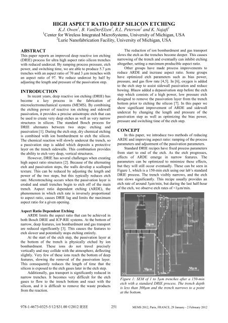
but they will still occur eventually. These can be seen in<br />
Figure 1, which is a 150-min etch using our lab’s standard<br />
DRIE process. The trench visibly narrows, and the etch<br />
rate slows significantly. This recipe usually provides an<br />
etch rate of around 3µm/min, but during the last half-hour<br />
of the etch, we observe etch rates of
Table 1: Detailed process information for 150-min etches using the original and final DRIE recipes. The final recipe<br />
ramps the process parameter values throughout the etch.<br />
Etch parameters<br />
Passivation parameters<br />
Recipe<br />
Step length (sec)<br />
Pressure<br />
(mTorr)<br />
Bias power (W) Step length (sec) Pressure (mTorr)<br />
Original 2 30 60 2.6 24<br />
Final<br />
(start end)<br />
2.6 5.6 30 15 60 140 2 3.5 24 34<br />
In order to reduce the ARDE effects, we tune three<br />
parameters of the etch cycle: bias power, etch step<br />
duration, and chamber pressure. Increasing the bias power<br />
during the first second of the etch step improves ion<br />
directionality and improves passivation breakthrough.<br />
Increasing the etch step duration gives more time to flow<br />
the etch gases to the trench bottom and etch the silicon.<br />
Decreasing pressure during the etch step reduces ion<br />
collisions, increasing the number of ions that reach the<br />
trench bottom, and improves gas transport in the trenches.<br />
However, it decreases the concentration of etch gases in<br />
the chamber, slightly decreasing the etch rate.<br />
At shallow depths, these adjustments to etch<br />
parameters are not necessary, and may in fact be<br />
detrimental to the etch characteristics. Higher power<br />
reduces mask selectivity greatly, increasing the etch time<br />
can cause undercut, and the lower power may reduce the<br />
etch rate. Instead of applying these adjustments for the<br />
entire etch, we ramp these parameters gradually and<br />
continuously over the duration of the etch. Thus the etch<br />
is better optimized at each etch depth as the etch proceeds.<br />
Some previous works have two or more sequential recipes<br />
to account for this [8], but by having the parameters vary<br />
continuously we can improve uniformity of the etch.<br />
Our second advancement is adjustment of the<br />
passivation step parameters to reduce undercut in the etch.<br />
Making the aforementioned changes to the etch<br />
parameters not only improves the etch rate at the trench<br />
bottom, but also at the top of the trench. The increased<br />
power can eat through the passivation layer near the top<br />
of the trench and begin to etch laterally. In order to<br />
compensate for this, we increase the passivation pressure<br />
and duration. Increasing the pressure provides more<br />
reactant, reinforcing the passivation layer on the trench<br />
sidewalls. Increasing the duration of the step results in a<br />
thicker passivation layer. As with the etch parameters, the<br />
passivation parameters are ramped gradually and<br />
continuously throughout the process.<br />
PROCESS DESCRIPTION<br />
For our testing, we use a mask with trenches varying<br />
from 1 µm to 10 µm in width. These are patterned into a<br />
5 µm-thick SPR220(3.0) photoresist mask using a GCA<br />
AS200 AutoStepper with 5:1 reduction.<br />
Because of the length and power of the DRIE<br />
process, a thick oxide mask is required in addition to the<br />
photoresist. A 4 µm layer, consisting of 2 µm thermal<br />
oxide and 2 µm LPCVD oxide is used. This oxide layer is<br />
etched using an SPTS glass etcher using a recipe designed<br />
for submicron features with high sidewall verticality.<br />
Other groups have used a hard aluminum mask [3,6].<br />
However, metal masks can cause loading and resputtering<br />
issues in high power ICP systems, and are more<br />
difficult to pattern than oxide masks. In order to increase<br />
the depth of our features, a metal mask could be<br />
considered in the future.<br />
The DRIE process, performed on an SPTS Pegasus<br />
system, starts with our standard etch designed for small<br />
features, and ramps the bias power, step durations, and<br />
process pressure throughout the etch. The final<br />
parameters, compared to the original parameters, are<br />
shown in Table 1.<br />
RESULTS<br />
Table 2 shows the effects of changing the various<br />
process parameters. Changing the bias power, which<br />
should improve passivation breakthrough, clearly<br />
improves the etch rate later in the process, but the trench<br />
still shows signs of narrowing. Increasing the etch<br />
duration at the end of the etch significantly reduces<br />
narrowing at the trench bottom, and also increases etch<br />
depth. Changing the etch pressure has the most dramatic<br />
effect on depth and narrowing, and when combined with<br />
the previous parameters provides very good results.<br />
However, it is clear that adjusting these parameters<br />
greatly increases the undercut at the top of the features.<br />
Ramping etch parameters<br />
By ramping the bias power, etch step duration, and<br />
etch pressure throughout the duration of the etch, we<br />
obtain very deep trench trenches: 335 µm for a 5.5 µm<br />
Table 2: Etch results varying different parameters.<br />
Values are for a 5µm mask opening.<br />
Parameter<br />
Adjusted<br />
Etch<br />
depth<br />
Trench<br />
bottom<br />
Undercut<br />
Original (150 min) 290µm closed 2.5µm<br />
Bias power ↑<br />
(90 min)<br />
230µm 1.8µm 1.2µm<br />
Etch step duration ↑<br />
(80 min)<br />
230µm 2.9µm 1.5µm<br />
Bias power ↑<br />
Duration ↑<br />
Pressure ↓<br />
335µm 7.2µm 3.5µm<br />
(120 min)<br />
Etch parameters +<br />
Pass. Parameters<br />
(120 min)<br />
330µm 5.2µm 2µm<br />
252
10µm<br />
5µm<br />
25µm 50µm<br />
50µm<br />
10µm<br />
Figure 2: SEM of 1 to 5 µm trenches after a 120-min<br />
etch ramping bias power, etch time, and etch<br />
pressure. Note the large undercut at the top (3.5 µm).<br />
trench after 120 min. However, the process results in a<br />
large undercut (greater than 3.5 µm per side) at the top of<br />
the trench. Trenches etched with this process for 120 min<br />
are shown in Figure 2.<br />
Ramping passivation parameters<br />
In order to significantly reduce the undercut at the top<br />
of the feature, we also ramp the duration and pressure of<br />
the passivation step. Using this technique, we fabricate<br />
the trenches shown in Figure 3 which have a similar depth<br />
but significantly reduced undercut (less than 2 µm per<br />
side). Figure 4 compares the undercut achieved with and<br />
without these passivation step adjustments.<br />
Figure 3: SEM of 1 to 5µm trenches after a 120-min<br />
etch also ramping passivation time and pressure. The<br />
undercut is reduced to less than 2µm.<br />
a 5 µm trench in [8]) and for a 3 µm trench the aspect<br />
ratio is 97.3. In [5], an aspect ratio of 107 is reported for a<br />
375 nm trench. Because aspect ratio tends to decrease<br />
with increasing trench width (Figure 6), this is<br />
comparable to our results.<br />
Additionally, we have shown that, while etch rate<br />
decreases over time, even for deep trenches it is still<br />
reasonably large: greater than 1.5 µm/min after 150 min<br />
for 4-5 µm trenches (Figure 7). Our aspect ratio is<br />
currently limited by the mask used to pattern the trenches.<br />
The current mask lasts for close to 180 min of etching. If<br />
we can improve our mask selectivity, we could etch<br />
longer and achieve higher aspect ratios.<br />
Final process<br />
With this revised process we have successfully etched<br />
trenches as narrow as 1 µm (190 µm deep) and as wide as<br />
10 µm (490 µm deep). Table 3 and Figure 5 present<br />
results of these trenches, which have been etched for 150<br />
min. We have achieved the highest aspect ratio for a given<br />
trench width ever reported in literature (Figure 6). For a<br />
5.7 µm trench, the aspect ratio is 69.8 (compared to 58 for<br />
4<br />
Undercut (μm)<br />
3<br />
2<br />
1<br />
before adjusting passivation<br />
after adjusting passivation<br />
0<br />
2 3 4 5 6<br />
Trench width (μm)<br />
Figure 4: Undercut before and after passivation step<br />
adjustment.<br />
50µm<br />
Figure 5: SEM of trenches after 150 min of etching.<br />
253
Table 3: Optimized etch characteristics including depth, aspect ratio, sidewall slope, and undercut vs. trench<br />
width. The etch time is 150 min.<br />
Mask<br />
opening<br />
Actual trench width (µm)<br />
Top Middle Bottom<br />
Trench<br />
depth (µm)<br />
Aspect<br />
ratio<br />
Sidewall<br />
slope (⁰)<br />
Undercut<br />
(µm)<br />
2.5 6.3 3 1.7 292 97.3 89.55 1.9<br />
3.5 7.4 3.9 2.5 339 86.9 89.59 1.95<br />
4.4 8.8 4.7 3.4 370 78.7 89.58 2.2<br />
5.3 10 5.7 4.2 398 69.8 89.58 2.35<br />
Aspect ratio<br />
150<br />
100<br />
50<br />
this work<br />
[3]<br />
[6]<br />
[4]<br />
0<br />
0 2 4 6 8 10 12<br />
Trench width (μm)<br />
Figure 6: Aspect ratio of adjusted recipe compared to<br />
state-of-the art.<br />
CONCLUSION<br />
We have developed an advanced DRIE process for<br />
etching ultra high aspect ratio features in silicon. By<br />
ramping the process parameters, including bias power,<br />
step duration, and pressure, we have significantly<br />
increased the achievable aspect ratio for trenches of 1 to<br />
10 µm width. We have shown aspect ratios of 69.8 for a<br />
5.7 µm trench, and up to 97.3 for a 3 µm trench.<br />
Additionally, by ramping the passivation parameters, we<br />
are able to decrease the undercut at the top of the trench to<br />
less than 2 µm for a 5 µm opening. With further<br />
optimization and an improved masking layer, we may be<br />
able to further improve the aspect ratio.<br />
ACKNOWLEDGEMENTS<br />
This work was done in the Lurie Nanofabrication<br />
Facility (LNF), a member of the National<br />
Nanotechnology Infrastructure Network, which is<br />
supported in part by the National Science Foundation.<br />
This project is funded by the MAST Program of the Army<br />
Research Lab (ARL) under Award Number W911NF-08-<br />
2-0004.<br />
REFERENCES<br />
[1] F. Laermer and A. Schilp, “Method of anisotropically<br />
etching silicon,” U.S. Patent 5501893, Mar. 26, 1996.<br />
[2] I. W. Rangelow, “Critical tasks in high aspect ratio<br />
silicon dry etching for microelectromechanical<br />
systems,” J. Vac. Sci. Technol. A, vol. 21, no. 4, pp.<br />
1550-1562, 2003.<br />
Etch rate (μm/min)<br />
4<br />
3<br />
2<br />
2.5μm<br />
1<br />
3.5μm<br />
4.4μm<br />
5.3μm<br />
0<br />
0 50 100 150<br />
Time (min)<br />
Figure 7: Etch rate over time for different trench<br />
widths.<br />
[3] J. Yeom, Y. Wu, J. C. Selby, and M. A. Shannon,<br />
“Maximum achievable aspect ratio in deep reactive<br />
ion etching of silicon due to aspect ratio dependent<br />
transport and the microloading effect,” J. Vac. Sci.<br />
Technol. B, vol. 23, no. 6, pp. 2319-2329, 2005.<br />
[4] W. J. Park, et al., “High aspect ratio via etching<br />
conditions for deep trench of silicon,” Surface and<br />
Coatings Technology, vol. 171, pp. 290-295, 2003.<br />
[5] F. Marty, et al., “Advanced etching of silicon based<br />
on deep reactive ion etching for high aspect ratio<br />
microstructures and three-dimensional micro- and<br />
nanostructures,” Microelectronics Journal, vol. 36,<br />
pp. 673-677, 2005.<br />
[6] C. K. Chung, H. C. Lu and T. H. Jaw, “High aspect<br />
ratio silicon trench fabrication by inductively coupled<br />
plasma,” Microsystem Technologies vol. 6, pp. 106-<br />
108, 2000.<br />
[7] M. A. Blauw, et al., “Advanced time-multiplexed<br />
plasma etching of high aspect ratio silicon<br />
structures,” J. Vac. Sci. Technol. B, vol. 20, pp. 3106-<br />
3110, 2002.<br />
[8] A. Kok, et al., “High aspect ratio deep RIE for novel<br />
3D radiation sensors in high energy physics<br />
applications,” IEEE Nuclear Science Sym. Conf.<br />
Record, 2009, pp. 1623-1627.<br />
CONTACT<br />
*K. Najafi, tel: +1-734-763-6650; najafi@umich.edu<br />
254
![[Sample B: Approval/Signature Sheet]](https://img.yumpu.com/34084789/1/190x245/sample-b-approval-signature-sheet.jpg?quality=85)