In-plane cavity-backed coplanar waveguide to rectangular ...
In-plane cavity-backed coplanar waveguide to rectangular ...
In-plane cavity-backed coplanar waveguide to rectangular ...

Create successful ePaper yourself
Turn your PDF publications into a flip-book with our unique Google optimized e-Paper software.
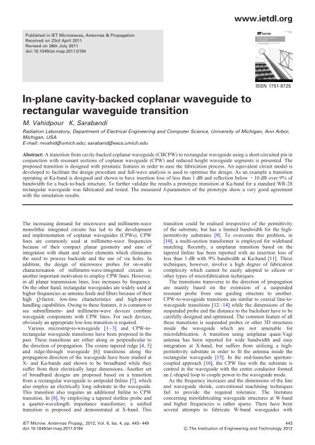
www.ietdl.orgPublished in IET Microwaves, Antennas & PropagationReceived on 23rd April 2011Revised on 26th July 2011doi: 10.1049/iet-map.2011.0194<strong>In</strong>-<strong>plane</strong> <strong>cavity</strong>-<strong>backed</strong> <strong>coplanar</strong> <strong>waveguide</strong> <strong>to</strong><strong>rectangular</strong> <strong>waveguide</strong> transitionM. Vahidpour K. SarabandiISSN 1751-8725Radiation Labora<strong>to</strong>ry, Department of Electrical Engineering and Computer Science, University of Michigan, Ann Arbor,Michigan, USAE-mail: mvahid@umich.edu; saraband@eecs.umich.eduAbstract: A transition from <strong>cavity</strong>-<strong>backed</strong> <strong>coplanar</strong> <strong>waveguide</strong> (CBCPW) <strong>to</strong> <strong>rectangular</strong> <strong>waveguide</strong> using a short-circuited pin inconjunction with resonant sections of <strong>coplanar</strong> <strong>waveguide</strong> (CPW) and reduced height <strong>waveguide</strong> segments is presented. Theproposed transition is designed with prismatic features in order <strong>to</strong> ease the fabrication process. An equivalent circuit model isdeveloped <strong>to</strong> facilitate the design procedure and full-wave analysis is used <strong>to</strong> optimise the design. As an example a transitionoperating at Ka-band is designed and shown <strong>to</strong> have insertion loss of less than 1 dB and reflection below 210 dB over 9% ofbandwidth for a back-<strong>to</strong>-back structure. To further validate the results a pro<strong>to</strong>type transition at Ka-band for a standard WR-28<strong>rectangular</strong> <strong>waveguide</strong> was fabricated and tested. The measured S-parameters of the pro<strong>to</strong>type show a very good agreementwith the simulation results.The increasing demand for microwave and millimetre-wavemonolithic integrated circuits has led <strong>to</strong> the developmentand implementation of <strong>coplanar</strong> <strong>waveguide</strong>s (CPWs). CPWlines are commonly used at millimetre-wave frequenciesbecause of their compact planar geometry and ease ofintegration with shunt and series elements which eliminatesthe need <strong>to</strong> process backside and the use of via holes. <strong>In</strong>addition, the design of microwave probes for on-wafercharacterisation of millimetre-wave-integrated circuits isanother important motivation <strong>to</strong> employ CPW lines. However,in all planar transmission lines, loss increases by frequency.On the other hand, <strong>rectangular</strong> <strong>waveguide</strong>s are widely used athigher frequencies as antenna feeds and filters because of theirhigh Q-fac<strong>to</strong>r, low-loss characteristics and high-powerhandling capabilities. Owing <strong>to</strong> these features, it is common <strong>to</strong>see submillimetre- and millimetre-wave devices combine<strong>waveguide</strong> components with CPW lines. For such devices,obviously an appropriate low-loss transition is required.Various microstrip-<strong>to</strong>-<strong>waveguide</strong> [1–3] and CPW-<strong>to</strong><strong>rectangular</strong><strong>waveguide</strong> transitions have been proposed in thepast. These transitions are either along or perpendicular <strong>to</strong>the direction of propagation. The cosine tapered ridge [4, 5]and ridge-through <strong>waveguide</strong> [6] transitions along thepropagation direction of the <strong>waveguide</strong> have been studied atX- and Ka-bands and shown <strong>to</strong> be broadband while theysuffer from their electrically large dimensions. Another se<strong>to</strong>f broadband designs are proposed based on a transitionfrom a <strong>rectangular</strong> <strong>waveguide</strong> <strong>to</strong> antipodal finline [7], whichalso employ an electrically long substrate in the <strong>waveguide</strong>.This transition also requires an additional finline <strong>to</strong> CPWtransition. <strong>In</strong> [8], by employing a tapered slotline probe anda quarter-wavelength impedance transformer, a unifiedtransition is proposed and demonstrated at X-band. Thistransition could be realised irrespective of the permittivityof the substrate, but has a limited bandwidth for the highpermittivitysubstrates [9]. To overcome this problem, in[10], a multi-section transformer is employed for widebandmatching. Recently, a uniplanar transition based on thetapered finline has been reported with an insertion loss ofless than 1 dB with 9% bandwidth at Ka-band [11]. Thesetechniques, however, involve a high degree of fabricationcomplexity which cannot be easily adopted <strong>to</strong> silicon orother types of microfabrication techniques.The transitions transverse <strong>to</strong> the direction of propagationare mainly based on the extension of a suspendedresonant probe from one guiding structure <strong>to</strong> another.CPW-<strong>to</strong>-<strong>waveguide</strong> transitions are similar <strong>to</strong> coaxial line-<strong>to</strong><strong>waveguide</strong>transitions [12–14] while the dimensions of thesuspended probe and the distance <strong>to</strong> the backshort have <strong>to</strong> becarefully designed and optimised. The common feature of allthese transitions is suspended probes or other 3D structuresinside the <strong>waveguide</strong> which are not amenable formicrofabrication. A transition using uniplanar quasi-Yagiantenna has been reported for wide bandwidth and easyintegration at X-band, but suffers from utilising a highpermittivitysubstrate in order <strong>to</strong> fit the antenna inside the<strong>rectangular</strong> <strong>waveguide</strong> [15]. <strong>In</strong> the end-launcher aperturecoupledapproach [16], the CPW line with the substrate iscentred in the <strong>waveguide</strong> with the centre conduc<strong>to</strong>r formedan L-shaped loop <strong>to</strong> couple power <strong>to</strong> the <strong>waveguide</strong> mode.As the frequency increases and the dimensions of the lineand <strong>waveguide</strong> shrink, conventional machining techniquesfail <strong>to</strong> provide the required <strong>to</strong>lerance. The literatureconcerning mirofabricating <strong>waveguide</strong> structures at W-bandand higher frequencies is rather sparse. There have beenseveral attempts <strong>to</strong> fabricate W-band <strong>waveguide</strong>s withIET Microw. Antennas Propag., 2012, Vol. 6, Iss. 4, pp. 443–449 443doi: 10.1049/iet-map.2011.0194 & The <strong>In</strong>stitution of Engineering and Technology 2012
www.ietdl.orglow-cost microfabrication techniques such as lithography [17,18]. However, in these techniques, the height of the<strong>waveguide</strong> is limited by the maximum thickness of the spunpho<strong>to</strong>resist, limiting the fabrication <strong>to</strong> the reduced-height<strong>waveguide</strong>s which suffer from high attenuation. Takingadvantage of the ‘snap-<strong>to</strong>gether’ technique, a <strong>rectangular</strong><strong>waveguide</strong> was fabricated in two halves and then the halveswere put <strong>to</strong>gether <strong>to</strong> form a complete <strong>waveguide</strong> [19–21].An alternate technique <strong>to</strong> etch the <strong>waveguide</strong> is deepreactive ion etching (DRIE) of silicon. Unlike wet etchingwhich is dependent on the crystal <strong>plane</strong>s of silicon, DRIE isisotropic and provides vertical sidewalls. Hence, DRIE is aviable approach for fabrication of a high-performancemicromachined <strong>waveguide</strong> structure. <strong>In</strong> [22, 23], a transitionusing microfabrication processes with separately fabricatedand assembled probe has been reported for both diamondand <strong>rectangular</strong> <strong>waveguide</strong> with 20% bandwidth. Anotherhigh-precision silicon micromachined transition with acapability <strong>to</strong> integrate filters has been proposed in [24, 25]and shows wideband characteristics at the same frequencyrange. However, limitations of microfabrication processesdo not allow fabricating many of the aforementionedtransitions because of the complexity of the geometriesand the number of steps needed in their assembly.<strong>In</strong> this study, we propose an in-<strong>plane</strong> <strong>cavity</strong>-<strong>backed</strong><strong>coplanar</strong> <strong>waveguide</strong> (CBCPW) line-<strong>to</strong>-<strong>rectangular</strong> <strong>waveguide</strong>transition with prismatic features that does not requiremultiple parts and complex assembly. <strong>In</strong> this approach, theneed for fabricating suspended probe is eliminated andeffective transition is achieved using two resonant structures,namely, shorted CPW line over the <strong>waveguide</strong> followed by anE-<strong>plane</strong> step discontinuity. Since the design is very simplewith the features aligned with the Cartesian coordinate <strong>plane</strong>s,it is highly compatible with microfabrication processes.However, it should be mentioned that since the design isusing short-circuited pin, the transition bandwidth issomewhat limited. The transition is modelled by an equivalentcircuit <strong>to</strong> help with the initial design which is then optimisedusing a full-wave analysis. To demonstrate the validity of thetransition and its model, a back-<strong>to</strong>-back structure is fabricatedby conventional machining methods at Ka-band and themeasurement results are compared <strong>to</strong> the simulations.1 Design considerations of <strong>waveguide</strong>transitionsTraditional transitions based on E-<strong>plane</strong> probe excitation ofthe <strong>waveguide</strong> mode involve attaching a suspended probe<strong>to</strong> the centre conduc<strong>to</strong>r of CPW or coaxial linesperpendicular <strong>to</strong> the broad wall of <strong>waveguide</strong>s as shown inFig. 1a. The suspended probes in <strong>waveguide</strong> can be viewedas an infinite array of dipoles and thus can be matched rathereasily <strong>to</strong> a coaxial line and provide octave bandwidth.The coaxial line-<strong>to</strong>-<strong>waveguide</strong> transitions are commonlyused at microwave frequencies since fabrication andassembly is rather straightforward. At high millimetre-waveand submillimetre-wave frequencies where dimensions arevery small, suspending small metalised probes and assemblywith the required <strong>to</strong>lerance is a challenging task. If the probeis extended, all the way <strong>to</strong> the lower plate of the <strong>waveguide</strong><strong>to</strong> form a shorting pin then the pin can be formed on samesubstrate and can be bonded <strong>to</strong> a <strong>to</strong>p substrate <strong>to</strong> make therequired electric connection. However, a short-circuitedprobe is not resonant, acts purely reactive and cannot bematched <strong>to</strong> the CPW line directly. <strong>In</strong> the next section, thearchitecture needed for making the transition from CPW <strong>to</strong><strong>rectangular</strong> <strong>waveguide</strong> using a shorting pin is described.2 Transition using a shorting pinTo properly excite a <strong>waveguide</strong> with a shorting pin, a resonantcondition must be achieved <strong>to</strong> eliminate the reactance of thepin. It is well known that a pin terminated by the broadwall of a <strong>rectangular</strong> <strong>waveguide</strong> acts as an inductiveelement whose inductance is inversely proportional <strong>to</strong> itsdiameter and the <strong>waveguide</strong> dimensions [26]. The geometryand the equivalent circuit model of a shorting pin areshown in Fig. 1b. For this case the transformer turn ratiocan be calculated from [27]√( )2a tan ka 2n =b ka(1)Fig. 1Design considerations of <strong>waveguide</strong> transitionsa Traditional resonant probe excitation for <strong>waveguide</strong>b Probe is terminated by the broad wall of the <strong>waveguide</strong>. <strong>In</strong> the equivalent circuit mode, L p is the equivalent inductance (X p ), C b is the series capacitance of theshort-circuited probe (X b ) [26] and Z 0 is the characteristic impedance of the <strong>waveguide</strong>c E-<strong>plane</strong> step discontinuity generates capacitances required for resonance needed for the mode conversion c the equivalent circuit model for the proposedresonanced The equivalent circuit model for the proposed resonance, X step is the equivalent capacitance of the step discontinuity444 IET Microw. Antennas Propag., 2012, Vol. 6, Iss. 4, pp. 443–449& The <strong>In</strong>stitution of Engineering and Technology 2012doi: 10.1049/iet-map.2011.0194
www.ietdl.orgwhere a and b are the width and height of the <strong>rectangular</strong><strong>waveguide</strong>, respectively, and k is the free spacewavenumber as described in [27]. The reactance X can beestimated by variational methods [27] and is capacitivebelow and inductive above the resonant frequency. Tocompensate for the inductance of the shorting pin X p , acapacitive element is needed. Since a step discontinuity inthe E-<strong>plane</strong> of the <strong>waveguide</strong> acts as a capacitive element, itcan be used <strong>to</strong> compensate for the inductive behaviour ofthe pin. That is, a resonant condition can be realised byterminating a short-circuited pin in a reduced-height<strong>waveguide</strong> with a step transition from the reduced-height<strong>waveguide</strong> <strong>to</strong> the standard-size <strong>waveguide</strong> as shown inFigs. 1c and d. The length of the <strong>waveguide</strong> between thepin and the step transition can be used <strong>to</strong> control thecapacitance seen by the inductance. Also, the <strong>waveguide</strong>height can be used <strong>to</strong> control the capacitance at the steptransition point. This structure eliminates the use ofsuspended probe for transition and is simple <strong>to</strong> fabricate.3 CBCPW <strong>to</strong> <strong>rectangular</strong> <strong>waveguide</strong>transitionCBCPW lines are preferred at very high frequencies formounting active components because of their low-losscharacteristics [28] (Fig. 2). Hence, a transition from alow-loss membrane-supported CBCPW <strong>to</strong> <strong>rectangular</strong><strong>waveguide</strong> is considered here. <strong>In</strong> this CBCPW, since thedielectric substrate is removed and the line is suspendedover a hollow trench, dielectric loss has been eliminated.Also, the conduc<strong>to</strong>r loss is decreased substantially byreducing the current density near the edges and distributingit more uniformly over the metallic strip and the groundaround it. For fabrication purposes, a dielectric membraneon <strong>to</strong>p of the line supports the suspended line over thetrench. This line can be easily incorporated with hollow<strong>rectangular</strong> <strong>waveguide</strong>s [28].To design the transition based on the idea of the shortcircuitedpin, first the dimensions of <strong>waveguide</strong> andCBCPW line are chosen based on the desired frequencyrange. The initial values of elements of the circuit modelare selected using the analytical formulas and measurementresults reported in [26, 27]. These values along with thelength of <strong>waveguide</strong> and CPW line sections are optimisedusing transmission line analysis of the circuit model <strong>to</strong>obtain the resonant behaviour. A structure based on thesevalues is designed and then optimised using full-wavesimula<strong>to</strong>r Ansoft HFSS.The proposed transition from CBCPW <strong>to</strong> <strong>rectangular</strong><strong>waveguide</strong> is presented in Figs. 3a and b. <strong>In</strong> this transition,three conversion steps are required: from CBCPW <strong>to</strong>conventional CPW inside the <strong>waveguide</strong>, CPW <strong>to</strong> reducedheight<strong>waveguide</strong> and reduced-height <strong>waveguide</strong> <strong>to</strong>standard <strong>waveguide</strong>. The CPW line is narrowed as it entersthe reduced-height <strong>waveguide</strong> in order <strong>to</strong> create atransmission line resona<strong>to</strong>r that includes the pin. A secondresona<strong>to</strong>r is created between the pin and the stepdiscontinuity inside the <strong>waveguide</strong>. The centre conduc<strong>to</strong>r ofthe CPW line is open circuited at the location of the pinand the pin is connected <strong>to</strong> the lower wall of a reducedheight<strong>waveguide</strong>. On the other side of the pin, thereduced-height <strong>waveguide</strong> is short circuited at a distance <strong>to</strong>appear as another reactance parallel <strong>to</strong> the pin inductance asshown in the equivalent circuit model in Fig. 3c. Thediscontinuity from CBCPW line <strong>to</strong> CPW line inside the<strong>waveguide</strong> is also modelled by a shunt capacitance.To demonstrate the performance of the proposed transitiona Ka-band pro<strong>to</strong>type is considered. The equivalent circuitmodel parameters are extracted as outlined before andthe S-parameters of a back-<strong>to</strong>-back structure from CBCPW<strong>to</strong> <strong>rectangular</strong> <strong>waveguide</strong> and <strong>rectangular</strong> <strong>waveguide</strong> <strong>to</strong>CBCPW based on the circuit model are shown in Fig. 3d.This design offers almost 9% of the bandwidth and lessthan 1 dB insertion loss. At the next step, Ansoft HFSS isused <strong>to</strong> analyse and optimise these values by adjustingthe lengths of transition line segments, the step height andthe pin thickness. The reflection coefficient of the optimisedstructure is compared <strong>to</strong> that of the circuit model for theback-<strong>to</strong>-back transition in Fig. 4. As shown, a goodagreement is obtained. It is also shown that the physicalstructure provides a better performance than the onepredicted by the circuit model. The electric field distributionof the optimised structure is shown in Fig. 5a andwell represents the conversion of the CPW mode <strong>to</strong>the <strong>waveguide</strong> mode using the terminated pin. Fig. 5brepresents the reflection and transmission coefficients of thistransition. It is observed that a transmission above 21 dBand reflection below 210 dB for more than 9% ofthe bandwidth can be achieved. An enlarged plot of thetransmission coefficient over the passband is also presentedin Fig. 5c.3.1 Bandwidth enhancementThe bandwidth of the transition is sufficient for mostapplication at these very high frequencies. However, insituations where more bandwidth is needed, the number ofshorting pins and step discontinuities can be increasedaccordingly.To add one more resonance, another shorting pin and stepdiscontinuity can be introduced. The geometry of a three-polestructure is shown in Fig. 6a. Since the height of the stepdiscontinuity is smaller which introduces smallercapacitance values, the pin must be thinner <strong>to</strong> provide aresonance value close <strong>to</strong> the previous ones. The dimensionsare optimised using Ansoft HFSS and the reflectioncoefficients of the structure are presented in Fig. 6b. Itisshown that the additional resonance increases the bandwidthup <strong>to</strong> about 15%.4 Fabrication and measurementFig. 2 Low-loss membrane supported <strong>cavity</strong>-<strong>backed</strong> CPW [28]<strong>In</strong> this line, the dielectric substrate is eliminated and the centre conduc<strong>to</strong>r issupported by a membrane on <strong>to</strong>p. The transition of this line <strong>to</strong> <strong>rectangular</strong><strong>waveguide</strong> is investigatedAs mentioned before, a dielectric membrane is used <strong>to</strong>support the <strong>to</strong>p suspended thin metal layer of CBCPW andprevent it from collapsing. The membrane covers theconduc<strong>to</strong>r and the structure cannot be fed by probes fromIET Microw. Antennas Propag., 2012, Vol. 6, Iss. 4, pp. 443–449 445doi: 10.1049/iet-map.2011.0194 & The <strong>In</strong>stitution of Engineering and Technology 2012
www.ietdl.orgFig. 3Proposed transition from CBCPW <strong>to</strong> <strong>rectangular</strong> <strong>waveguide</strong>a CBCPW <strong>to</strong> <strong>rectangular</strong> <strong>waveguide</strong> transition. It includes a transition from CBCPW <strong>to</strong> CPW, CPW <strong>to</strong> reduced-height <strong>waveguide</strong> mode and reduced-height<strong>waveguide</strong> mode <strong>to</strong> standard <strong>waveguide</strong> modeb Top view, side view and a side view of the back-<strong>to</strong>-back structurec Equivalent circuit model for the transition for Z CBCPW ¼ 50 V, Z CPW ¼ 85 V, X t ¼ 2j 140 V, X ¼ 2j 110 V, n ¼ 1, X b ¼ 2j 8 V, X p ¼ +j 58 V,X step ¼ 2j 1000 V, l backshort ¼ 5mm¼ l g /3, l 2 ¼ 10 mm ¼ 2l g /3, l 3 ¼ 17 mm. Waveguide dimensions are set as the standard dimensions of WR-28Ka-band <strong>waveguide</strong>sd Reflection and transmission coefficients of the circuit model of the back-<strong>to</strong>-back structure for the initial values of the elements <strong>to</strong> achieve a low conversion lossFig. 4 Optimised transition with HFSS is compared <strong>to</strong> the initialdesign based on the circuit model for a back-<strong>to</strong>-back transitionand shows good agreement and improved performancethe <strong>to</strong>p. Basically the <strong>to</strong>p layer and the membrane areprotecting the active components that excite or receive the<strong>waveguide</strong> signal. <strong>In</strong> order <strong>to</strong> test the transition and be able<strong>to</strong> make contact <strong>to</strong> the probe, the <strong>to</strong>p layer of the membraneis also patterned with a CPW line and is connected <strong>to</strong> thebot<strong>to</strong>m layer through via holes as shown in Fig. 7. Withthis transition, the structure can be fed from the <strong>to</strong>p by50 V GSG probes.To fabricate this structure at Ka-band, the lower partsincluding the CBCPW, reduced-height <strong>waveguide</strong> andstandard-height <strong>waveguide</strong> are machined on an ultramachinablealloy 360 brass plate and are gold-plated <strong>to</strong>prevent oxidation. Rogers Duroid 5880 with 1/4 oz (8mm)electrodeposited copper foil is used as the <strong>to</strong>p cover of the<strong>waveguide</strong> as well as the membrane for CBCPW. Thethickness of the substrate is chosen <strong>to</strong> be 0.127 mm (5 mil),thin enough <strong>to</strong> act as the membrane. Both sides of thesubstrate are patterned and connected by metalised via holesas shown in Fig. 7. Additional vias are drilled in thesubstrate in order <strong>to</strong> suppress the substrate mode. Thefabricated parts are represented in Fig. 8.446 IET Microw. Antennas Propag., 2012, Vol. 6, Iss. 4, pp. 443–449& The <strong>In</strong>stitution of Engineering and Technology 2012doi: 10.1049/iet-map.2011.0194
www.ietdl.orgFig. 5The optimised structurea Electric field distribution at 30 GHz for a back-<strong>to</strong>-back transition with S 1 ¼ 1.46 mm, W 1 ¼ 0.37 mm, S 2 ¼ 0.972 mm, W 2 ¼ 0.247 mm, W WG ¼ 7.112 mm,h WG ¼ 3.556 mm, h 1 ¼ 0.379 mm, h 2 ¼ 1.65 mm, t ¼ 0.49 mm, l 1 ¼ 5.024 mm, l 2 ¼ 9.97 mm and l 3 ¼ 16.8 mmb Side view: E-<strong>plane</strong> cross section (<strong>waveguide</strong> centre at maximum E-field)c Reflection and transmission coefficients for the back-<strong>to</strong>-back transition at Ka-bandd Transmission coefficient at the passbandDifferent techniques were tested <strong>to</strong> bond the substrate <strong>to</strong> thebrass unit. <strong>In</strong>itially solder paste and silver epoxy were used.However, since a high temperature is needed for pastesand epoxies, the substrate was warped and damaged, andthe brass unit was oxidised. Also, the results were notsatisfac<strong>to</strong>ry because of misalignments and air gaps aroundthe edges. <strong>In</strong> addition, the solder reflow caused shortcircuits in the substrate during the bonding process.Moreover, many times the thin pins were bent and easilyFig. 6Bandwidth enhancementa Proposed three-pole structure for enhanced bandwidthbS-parameters of the transitionBandwidth of the transition is increased <strong>to</strong> about 15% as a result of having athree-pole structure by adding one resonance, a shorting pin and a stepdiscontinuity with h 3 ¼ 2.26 mm, l 1 ¼ 5 mm, l 2 ¼ 10 mm, l 4 ¼ 3.3 mm,l 5 ¼ 6 mm. Additional resonances can be introduced for further enhancement.broken during bonding at high temperatures. The best resultswere obtained by screwing the two units <strong>to</strong>gether. Since thesubstrate is very thin, a thick metal plate is used on <strong>to</strong>p of it<strong>to</strong> ensure that sufficient pressure is applied <strong>to</strong> the substrateand brass unit <strong>to</strong> prevent possible air gaps. The silver-platedlong rigid steel wires are snapped in<strong>to</strong> holes drilled on thebot<strong>to</strong>m of the reduced-height <strong>waveguide</strong> and soldered. Thepins pass through holes cut on the substrate <strong>to</strong> facilitatealignment of the substrate and the unit.After bonding, the structure is fed by ground-signal-ground(GSG) probes connected <strong>to</strong> the network analyser using Kabandflexible cables. Prior <strong>to</strong> measurement it is essentialthat the probes and cables be calibrated. For this purpose,on-substrate thru-reflect-line (TRL) calibration lines aresimulated and designed. For TRL calibration, threecalibration standards are fabricated on the same substrate.These include two line segments with known phase shiftsfor thru measurements and an open-ended line with aknown electrical length for reflection measurement. Aftercalibration, S-parameters of the transition are measured andpresented in Fig. 9. The measurement results show a goodagreement with the simulation, around 9% of the bandwidthbelow 210 dB for return loss and over 21 dB for insertionloss. The observed deviations from the simulation areattributed <strong>to</strong> misalignment, especially near the pin positionsand possible air gaps between the substrate and the brassunit. The air gap should be of lesser concern since screwsconnecting the substrate <strong>to</strong> the brass unit should applyenough pressure <strong>to</strong> make good metal-<strong>to</strong>-metal contact.Since alignment is done with hand, small misalignment canlead <strong>to</strong> small deviations from the ideal response. Toexamine this hypothesis, a simulation was carried out wherethe <strong>to</strong>p substrate was shifted <strong>to</strong> one side by a very smallamount <strong>to</strong> produce about 300 mm translational displacementat the pin position. This is a typical length that might bemisaligned by manually aligning. Fig. 10 shows theIET Microw. Antennas Propag., 2012, Vol. 6, Iss. 4, pp. 443–449 447doi: 10.1049/iet-map.2011.0194 & The <strong>In</strong>stitution of Engineering and Technology 2012
www.ietdl.orgFig. 7CPW <strong>to</strong> CBCPW transitiona Transition from a 50 V CPW line patterned on <strong>to</strong>p of the substrate <strong>to</strong> the CBCPW line patterned on the bot<strong>to</strong>m layer. Lines are connected through electroplated via holesb Side viewFig. 8Fabricated partsa CBCPW trench, reduced-height <strong>waveguide</strong> and the standard <strong>waveguide</strong> are machined on a brass plateb Top cover includes the lines is a substrate whose both sides are etched with CPW patternsFig. 9Simulation compared <strong>to</strong> measurement resultsa Reflection coefficientb Transmission coefficientBoth show a good agreement with the simulation. Observed deviations from the simulation are attributed <strong>to</strong> misalignment, especially near the pin positions andpossible air gaps between the substrate and the brass unitsimulation results for the misaligned structure where it isshown that the transmission has decreased specifically forfrequencies lower than 29 GHz. Also, the impedance matchnear 31 GHz is not as good as what the structure is capableof producing. This is very similar <strong>to</strong> the measured resultsindicating that even careful hand alignment is not goodenough <strong>to</strong> achieve the best performance this transition canproduce at Ka-band. To achieve better results, a betteralignment approach will be needed. For the ultimateapplication of this transition at Y-band wafer alignmentapproaches in clean rooms are available for achievingalignment accuracy down <strong>to</strong> 1 mm.448 IET Microw. Antennas Propag., 2012, Vol. 6, Iss. 4, pp. 443–449& The <strong>In</strong>stitution of Engineering and Technology 2012doi: 10.1049/iet-map.2011.0194
www.ietdl.orgFig. 10 Simulation results of a structure with misalignments (300 mm translational displacement) between the <strong>to</strong>p substrate and the brass unitcompared <strong>to</strong> the measured resultsTransmission is decreased for frequencies lower than 29 GHz and the impedance match near 31 GHz is not as good as that of the optimised5 ConclusionWe demonstrated a very simple and easy-<strong>to</strong>-fabricateCBCPW line <strong>to</strong> <strong>rectangular</strong> <strong>waveguide</strong> transition withprismatic features. The transition is based on the idea ofresonance excitation but does not include a suspendedprobe which was involved in the previous transitions.Using a short-circuited pin makes the transition amenablefor machining and micromachining techniques with fine<strong>to</strong>lerance needed for millimetre- and submillimetre-waveapplications. An equivalent circuit model, in which lumpedelements model the discontinuities and transitions, wasdeveloped for the initial design. A back-<strong>to</strong>-back structurefrom CBCPW <strong>to</strong> <strong>waveguide</strong> and <strong>waveguide</strong> <strong>to</strong> CBCPWwas then designed, optimised and fabricated at Ka-band <strong>to</strong>validate the results. The insertion loss below 1 dB andreflection of less than 210 dB over more than 9% ofbandwidth has been achieved. The bandwidth enhancementwas shown by introducing an additional resonance.6 References1 Reig, C., Navarro, E.A., Such, V.: ‘Full-wave FDTD design and analysisof wideband microstrip-<strong>to</strong>-<strong>waveguide</strong> transitions’, Microw. Opt.Technol. Lett., 2003, 38, pp. 317–3202 Grabherr, W., Huder, W.G.B., Menzel, W.: ‘Microstrip <strong>to</strong> <strong>waveguide</strong>transition compatible with MM-wave integrated circuits’, IEEE Trans.Microw. Theory Tech., 1994, 42, pp. 1842–18433 Kim, J.P., Park, W.S.: ‘Network analysis of inclined microstrip-slotlinetransitions’, IEE Proc. Microw. Antennas Propag., 2000, 147,pp. 412–4164 Ponchak, G.E., Simons, R.: ‘A new <strong>rectangular</strong> <strong>waveguide</strong> <strong>to</strong> CPWtransition’. IEEE Microwave Theory Tech. <strong>In</strong>t. Microwave Symp.Digest, 1990, vol. 1, pp. 491–4925 Dalman, C.: ‘New <strong>waveguide</strong> <strong>to</strong> <strong>coplanar</strong> <strong>waveguide</strong> transition forcentimetre and millimeter wave application’, Electron. Lett., 1990, 26,pp. 830–8316 Godshalk, E.M.: ‘A V-band wafer probe using ridge-through<strong>waveguide</strong>’, IEEE Trans. Microw. Theory Tech., 1991, 39,pp. 2218–22287 de Mingo, J., Moliner, A., Cameron, A.: ‘Waveguide-<strong>to</strong>-coupled fin-linetransition in Ka Band’, IEEE Microw. Guid. Wave Lett., 1996, 6,pp. 363–3658 Lin, T., Wu, R.: ‘CPW <strong>to</strong> <strong>waveguide</strong> transition with tapered slotlineprobe’, IEEE Microw. Wirel. Compon. Lett., 2001, 11, pp. 314–3169 Lin, T., Wu, R.: ‘A broadband microstrip-<strong>to</strong>-<strong>waveguide</strong> transition withtapered CPS probe’. Proc. 32nd European Microwave Conf., Milan,Italy, 2002, pp. 1–410 Hung, C., Liu, A.-S., Chien, C.-H., Wang, C.-L., Wu, R.B., et al.:‘Bandwidth enhancement on <strong>waveguide</strong> transition <strong>to</strong> conduc<strong>to</strong>r<strong>backed</strong> CPW with high dielectric constant substrate’, IEEE Microw.Wirel. Compon. Lett., 2005, 15, pp. 128–18011 Ramdane, A., Richalot, E., Picon, O., Puech, J., Lapierre, L.:‘Rectangular <strong>waveguide</strong> <strong>to</strong> CPW transition without air-bridge in theKa-band’, Microw. Opt. Technol. Lett., 2007, 49, pp. 510–51312 Ho, T.Q., Shih, Y.: ‘Spectral-domain analysis of E-<strong>plane</strong> <strong>waveguide</strong> <strong>to</strong>microstrip transitions’, IEEE Trans. Microw. Theory Tech., 1989, 37,pp. 388–39213 Cavanna, T., Linkowski, J.R., Suriani, A.: ‘Novel W-band hermetic<strong>waveguide</strong>-<strong>to</strong>-<strong>coplanar</strong> transition’. Third ESA Workshop onMillimeter Wave Technology and Applications, Espoo, Finland, May200314 Cavanna, T., Franzese, E., Limiti, E., Pelosi, G., Selleri, S., Suriani, A.:‘Coplanar-<strong>to</strong>-<strong>rectangular</strong> <strong>waveguide</strong> millimeter-wave transitionsmanufacturing <strong>to</strong>lerance analysis’, <strong>In</strong>t. J. RF Microw. Comput. AidedEng., 2006, 16, pp. 118–12415 Kaneda, N., Qian, Y., I<strong>to</strong>h, T.: ‘A broadband CPW-<strong>to</strong>-<strong>waveguide</strong>transition using quasi-Yagi antenna’. IEEE Microwave TheoryTechnology <strong>In</strong>t. Microwave Symp. Digest, Bos<strong>to</strong>n, MA, 2000, vol. 2,pp. 617–62016 Simons, R.N., Taub, S.R.: ‘New <strong>coplanar</strong> <strong>waveguide</strong> <strong>to</strong> <strong>rectangular</strong><strong>waveguide</strong> end launcher’, Electron. Lett., 1992, 28, (12), pp. 1138–113917 Digby, J.W., Mc<strong>In</strong><strong>to</strong>sh, C.E., Parkhurst, G.M., et al.: ‘Fabrication andcharacterization of micromachined <strong>rectangular</strong> <strong>waveguide</strong> componentsfor use at millimeter-wave and terahertz frequencies’, IEEE Trans.Microw. Theory Tech., 2000, 48, pp. 1293–130218 Collins, C.E., Miles, R.E., Digby, J.W., et al.: ‘A new micro-machinedmillimeter-wave and terahertz snap<strong>to</strong>gether <strong>rectangular</strong> <strong>waveguide</strong>technology’, IEEE Microw. Guid. Wave Lett., 1999, 9, pp. 63–6519 Hesler, J.L., Jui, K., Dahlstrom, R.K., et al.: ‘Analysis of an octagonalmicromachined horn antenna for submillimeter-wave applications’,IEEE Trans. Antennas Propag., 2001, 49, pp. 997–100120 Hui, K., Hesler, J.L., Kurtz, D.S., Bishop, W.L., Crowe, T.W.: ‘Amicromachined 585 GHz schottky mixer’, IEEE Microw. Guid. WaveLett., 2000, 10, pp. 374–37621 McGrath, W.R., Walker, C., Yap, M., Tai, Y.-C.: ‘Silion micromachined<strong>waveguide</strong>s for millimeter-wave and submillimeter-wave frequencies’,IEEE Microw. Guid. Wave Lett., 1993, 3, pp. 61–6322 Becker, J.P., Lee, Y., East, J.R., Katehi, L.P.B.: ‘A finite ground<strong>coplanar</strong> line-<strong>to</strong>-silicon micromachined <strong>waveguide</strong> transition’, IEEETrans. Microw. Theory Tech., 2001, 49, p. 200123 Lee, Y., Becker, J.P., East, J., Katehi, L.P.B.: ‘Fully micromachinedfinite-ground <strong>coplanar</strong> line-<strong>to</strong>-<strong>waveguide</strong> transitions for w-bandapplications’, IEEE Trans. Microw. Theory Tech., 2004, 52,pp. 1001–100724 Li, Y., Pan, B., Tentzeris, M.M., Papapolymerou, J.: ‘A fullymicromachined W-band <strong>coplanar</strong> <strong>waveguide</strong> <strong>to</strong> <strong>rectangular</strong> <strong>waveguide</strong>transition’. Proc. 2007 IEEE-IMS Symp., Honolulu, Hi, June 200725 Li, Y., Pan, B., Lugo, C., Tentzeris, M.M., Papapolymerou, J.: ‘Designand characterization of a W-band micromachined <strong>cavity</strong> filter includinga novel integrated transition from CPW feeding lines’, IEEE Trans.Microw. Theory Tech., 2007, 55, pp. 2902–291026 Marcuvitz, N.: ‘Waveguide handbook’ (McGraw-Hill, New York,1951), pp. 271–27327 Harring<strong>to</strong>n, R.F.: ‘Time-harmonic electromagnetic fields’ (McGraw-Hill, New York, 1961), pp. 177–179. 425–42828 Moallem, M., East, J., Sarabandi, K.: ‘Optimally designed membranesupportedgrounded CPW structure for submillimeter-waveapplications’. <strong>In</strong>t. Symp. Antennas Propagation, Charles<strong>to</strong>n, NC, 2009IET Microw. Antennas Propag., 2012, Vol. 6, Iss. 4, pp. 443–449 449doi: 10.1049/iet-map.2011.0194 & The <strong>In</strong>stitution of Engineering and Technology 2012

![[Sample B: Approval/Signature Sheet]](https://img.yumpu.com/34084789/1/190x245/sample-b-approval-signature-sheet.jpg?quality=85)