electrostatically driven micro-hydraulic actuator arrays
electrostatically driven micro-hydraulic actuator arrays
electrostatically driven micro-hydraulic actuator arrays

You also want an ePaper? Increase the reach of your titles
YUMPU automatically turns print PDFs into web optimized ePapers that Google loves.
ELECTROSTATICALLY DRIVEN<br />
MICRO-HYDRAULIC ACTUATOR ARRAYS<br />
Mahdi Sadeghi, Hanseup Kim, and Khalil Najafi<br />
Center for Wireless Integrated Microsystems (WIMS), University of Michigan, USA<br />
ABSTRACT<br />
This paper describes an all-electrical individuallyaddressable<br />
<strong>micro</strong>-<strong>hydraulic</strong> <strong>actuator</strong> array that<br />
produces high displacement and force by utilizing<br />
<strong>hydraulic</strong> amplification and electrostatic control,<br />
offering a considerable improvement in fabrication<br />
technique and performance over the recentlyintroduced<br />
<strong>micro</strong>-piston <strong>hydraulic</strong> <strong>actuator</strong> array<br />
[1,2]. The fabricated <strong>micro</strong> system consists of 3×3<br />
and 4×4 <strong>arrays</strong> of <strong>actuator</strong> cells. A curved electrode<br />
capacitive <strong>actuator</strong> with a diameter of 2236 μm<br />
<strong>driven</strong> at 200 V produces 30.0 μm deflection on the<br />
front side at 14.4 kPa of pressure which corresponds<br />
to 11.3 mN force generated by the capacitive <strong>actuator</strong><br />
on the back side. Actuation occurs from DC to 15 Hz.<br />
INTRODUCTION<br />
High-force, large-deflection <strong>actuator</strong>s are critical for<br />
devices such as valves and pumps used in<br />
<strong>micro</strong>fluidic systems, for surface bump manipulation<br />
in tactile displays, and <strong>micro</strong>-airfoil control. Table 1<br />
lists potential actuation methods.<br />
Table 1: Comparison of several actuation methods.<br />
E.S. Hydra. Piezo. Pneu. E.M.<br />
Force Low High High High High<br />
Deflection Small Large Small Large Large<br />
Fabrication<br />
& Materials<br />
Easy Difficult Difficult Difficult Difficult<br />
Power Low High Low High High<br />
Control Easy Easy Medium Easy Hard<br />
Speed Fast Medium Fast Slow Fast<br />
* E.S.=electrostatic; Hydra=<strong>hydraulic</strong>; Piezo=piezoelectric; Pneu=<br />
Pneumatic; E.M.=electro-magnetic<br />
Electrostatic actuation cannot provide the high forces<br />
(~10-100 mN) required for many applications.<br />
Techniques capable of high force suffer from control<br />
difficulties (E.M.) or are limited to small deflections<br />
(Piezo.). This raises a need for a new class of<br />
<strong>actuator</strong>s that offers controllable and high force<br />
actuation which can be delivered across a large<br />
displacement range. Our approach is to assist<br />
electrostatic actuation with <strong>hydraulic</strong> amplification.<br />
The E.S. mechanism allows for low power actuation<br />
and excellent control, while the <strong>hydraulic</strong> system<br />
provides large deflection and high force actuation.<br />
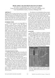
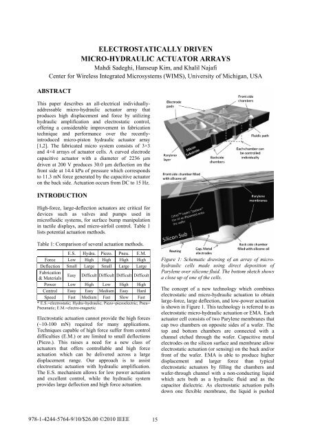
Figure 1: Schematic drawing of an array of <strong>micro</strong><strong>hydraulic</strong><br />
cells made using direct deposition of<br />
Parylene over silicone fluid. The bottom sketch shows<br />
a close up of one of the cells.<br />
The concept of a new technology which combines<br />
electrostatic and <strong>micro</strong>-<strong>hydraulic</strong> actuation to obtain<br />
large-force, large deflection, and low-power actuation<br />
is shown in Figure 1. This technology is referred to as<br />
electrostatic <strong>micro</strong>-<strong>hydraulic</strong> actuation or EMA. Each<br />
<strong>actuator</strong> cell consists of two Parylene membranes that<br />
cap two chambers on opposite sides of a wafer. The<br />
top and bottom chambers are connected with a<br />
channel etched through the wafer. Capacitive metal<br />
electrodes on the silicon surface and membrane allow<br />
electrostatic actuation (or sensing) on the back and/or<br />
front of the wafer. EMA is able to produce higher<br />
displacement and larger force than typical<br />
electrostatic <strong>actuator</strong>s by filling the chambers and<br />
wafer-through channel with a non-conducting liquid<br />
which acts both as a <strong>hydraulic</strong> fluid and as the<br />
capacitor dielectric. As electrostatic actuation pulls<br />
down one flexible membrane, the liquid is pushed<br />
978-1-4244-5764-9/10/$26.00 ©2010 IEEE 15
into the opposite chamber, causing its membrane to<br />
be deflected out of plane.<br />
By varying the area of the front and back side<br />
chambers, amplification of either force or<br />
displacement is achievable. Furthermore, by carefully<br />
choosing the <strong>hydraulic</strong> liquid we can take advantage<br />
of its high dielectric constant to increase the<br />
electrostatic force (capacitance).<br />
In previously published piston <strong>arrays</strong>, cross talk is<br />
inevitable due to use of a single large actuating<br />
chamber on one side of the wafer for actuating all of<br />
the cells in an array on the opposite side of the wafer,<br />
where the small membranes were latched whenever<br />
they were supposed to be at rest [1]. In that design,<br />
the single chamber provides fluidic connections<br />
between the cells during operation, causing crosstalk.<br />
In the new design presented here, each cell is<br />
actuated by its own membrane, minimizing cross talk<br />
between adjacent cells and eliminating the<br />
previously-required dual-side control electrodes. In<br />
addition, the wafer-level fabrication process and shift<br />
from piezoelectric to electrostatic actuation makes<br />
this architecture applicable to a variety of platforms.<br />
For example, external pneumatic devices are widely<br />
used in fluidic devices, since they can provide high<br />
force and large displacement. The EMA design<br />
shown here can provide almost the same<br />
performance, but additionally can be integrated with<br />
other MEMS devices such as <strong>micro</strong>-fluidics on a<br />
single wafer if the proper sequence of fabrication<br />
steps is chosen.<br />
FABRICATION PROCESS<br />
The fabrication process is based on a wafer level<br />
technique for bubble-free encapsulation of a liquid<br />
dielectric that provides the option of having<br />
individual actuated chambers for each of the cells.<br />
The chosen liquid dielectric material is<br />
polytrimethylsiloxane (Silicone oil 1,3,5-trimethyl-<br />
1,1,3,5,5-pentaphenyltrisiloxane) which has a vapor<br />
pressure at room temperature of under 1 mTorr, so<br />
that it can survive the low vacuum inside the<br />
Parylene deposition system [3]. After the oil is<br />
dispensed onto the wafer in the designated locations,<br />
the wafer is loaded in the Parylene deposition tool,<br />
and Parylene is deposited. The polymer conformally<br />
coats the oil on both sides of the wafer, encapsulating<br />
it [3]. Note that almost no leakage or evaporation of<br />
the liquid dielectric is expected during <strong>micro</strong>-system<br />
use since the silicone oil does not evaporate at<br />
atmospheric pressure and room temperature.<br />
Figure 2: Fabrication process.<br />
The fabrication process is shown in Figure 2. It<br />
begins with 3-4 μm dry etching of silicon to form a<br />
recess. This shallow recess plays an important role<br />
during liquid dispensing, as described later. Cr/Au<br />
electrodes are then deposited and patterned. Next,<br />
Cytop TM , an amorphous fluorocarbon polymer that is<br />
transparent and has low gas permeability, is spun,<br />
cured and then patterned with oxygen plasma on both<br />
sides. This hydrophobic layer of Cytop TM repels<br />
silicone oil. As a result, when the oil is later<br />
dispersed, it will be contained within the patterned<br />
Cytop TM -free areas. These areas, which are covered<br />
with oil and then Parylene, will define the chambers<br />
and actuating membranes. After Cytop TM deposition<br />
and patterning, a wafer-through DRIE step connects<br />
the front and backside chambers. The silicone liquid<br />
is then dispensed and is kept in place on the wafer’s<br />
surface by the Cytop TM layer. Although the etchedthrough<br />
channels connect the two sides of the wafer,<br />
the surface tension at the bottom side, resulting from<br />
the effective contact angle modification at the edge of<br />
the shallow trench, prevents the liquid from flowing<br />
out and provides a way to obtain different initial<br />
shapes of the Parylene membranes on the top and<br />
bottom sides.<br />
In a single Parylene deposition run, the dielectric<br />
liquid is encapsulated on both sides. The Parylene<br />
deposition is done while the wafer is flipped over in<br />
the deposition chamber, so that the back side faces<br />
up. Figure 3 shows the top and bottom view of one of<br />
the <strong>actuator</strong>s <strong>arrays</strong> made using this technique after<br />
Parylene deposition over the dispensed liquid. This<br />
encapsulation is bubble free since the deposition of<br />
16
the Parylene layer is conformal and done in the<br />
vacuum. In the last step, second capacitive electrodes<br />
are deposited using an appropriate shadow mask in an<br />
e-beam evaporator. For this layer of metal, Cr/Au is<br />
again used but the thickness of this second electrode<br />
is less than a fifth of that used for the first electrode.<br />
This precaution is taken to ensure that the actuating<br />
membrane is not too thick nor too rigid.<br />
Figure 3: Image of front and back side of the wafer<br />
after Parylene deposition but before the second metal<br />
layer is deposited. The oil is kept in place during<br />
Parylene deposition.<br />
Figure 4: Full wafer view (back side), showing that<br />
the introduced fabrication technique can be<br />
processed at the wafer level. The high yield of the<br />
method also can be observed.<br />
In Figure 4, images of a completed 100-mm wafer<br />
with <strong>arrays</strong> of <strong>actuator</strong>s show that this wafer-level<br />
technique has high-yield. One other important<br />
feature of this <strong>actuator</strong> structure is its robustness<br />
toward any harsh environmental disturbance (e.g.<br />
wind, rain etc.) by which the capacitive gap might be<br />
breached or collapsed. In conventional E.S. actuation,<br />
the gap is exposed, making the device susceptible to<br />
disturbance. In contrast, in the EMA structure the gap<br />
is filled with liquid and is encapsulated by the<br />
Parylene membranes.<br />
EXPRIMENTAL RESULTS<br />
Table 2 lists measured dimensions of several<br />
fabricated devices. By modifying the process, the<br />
curvature radius of the back chamber membrane was<br />
increased by almost 9x from the first batch of devices<br />
(Device 1-2) to the second batch (Device 2-2), for the<br />
same membrane radius. This results in a significant<br />
improvement in performance of the <strong>actuator</strong> cells.<br />
Table 2: Dimensions of the fabricated devices along<br />
with the measured height of the membranes and<br />
calculated curvature radii.<br />
D f [μm] D b [μm] h b [μm] R C,b [mm]<br />
Dev 1-1 2000 4472 264 9.59<br />
Dev 1-2 1000 2236 163 3.91<br />
Dev 2-1 2000 4472 62.4 37.7<br />
Dev 2-2 1000 2236 19.0 32.8<br />
Dev 2-3 500 1118 7.04 21.0<br />
* D f and D b are the diameters of the front and back side chambers,<br />
respectively. R C,b and h b are the curvature radius and height of the<br />
back side membrane.<br />
Among all the parameters, the curvature radius of the<br />
silicone oil bubble is very important since it strongly<br />
influences the electrostatic force generation. For a<br />
curved electrode with low curvature radius, a higher<br />
voltage is needed to generate the same force<br />
compared to an identically sized electrode with a<br />
higher curvature radius. In order to achieve higher<br />
curvature radius and thus get higher force at lower<br />
applied voltage, we made a shallow recess on the<br />
backside in the locations of the chambers. This recess<br />
has the same pattern as the Cytop TM creating a step at<br />
its edge. This step helps to keep the liquid in place.<br />
Combined with the hydrophobicity of Cytop TM , less<br />
liquid oil is needed to cover the chamber areas, which<br />
means the oil bubble’s height is lesser and the<br />
curvature radius is increased. The recess formation is<br />
done prior to Cr/Au deposition. As noted in Table 2,<br />
this process significantly increases the curvature<br />
radius from 3.91 mm in Device 1-2 to 32.8 mm in<br />
Device 2-2.<br />
Deflection of the back side membrane vs. applied<br />
voltage is shown in Figures 5 and 6. As the voltage<br />
increases, the membrane deflection increases and its<br />
shape changes. At 200 V the membrane partially<br />
sinks and partially bulges. However, an analysis of<br />
the volumetric change proves that despite this, a net<br />
volume is transferred to the other side. This volume<br />
dislocation results in force transfer from one side to<br />
17
the other. Furthermore, volume transfer was observed<br />
for actuation voltages from DC to 15 Hz ac.<br />
0V<br />
150V<br />
100V<br />
200V<br />
shown in Table 3, the normalized force generated by<br />
the hybrid EMA structure is almost 30 times larger<br />
than that of an air-gap capacitor with the same<br />
electrode curvature.<br />
Table 3: Normalized force generated by three<br />
capacitive <strong>actuator</strong>s. Dimensions match fabricated<br />
devices: membrane radius of 2200 μm, curvature<br />
radius of 33 mm, and gap around the edge of the<br />
curved electrode of 5.4 μm. The <strong>hydraulic</strong><br />
amplification factor is assumed to be 10.<br />
Curved<br />
electrode,<br />
Air gap<br />
Flat<br />
electrode.<br />
Air gap<br />
Curved<br />
electrode,<br />
Liq. gap,<br />
Hyd. Amp<br />
Force/ ε 0 V 2 1.92 e4 6.52 e4 5.74 e5<br />
CONCLUSION<br />
Figure 5: 3-D surface profiles of one of the cells of<br />
device 2-2 at 0, 100, 150 and 200 V. The pictures<br />
show the gradual deflection of the membrane as the<br />
voltage increases.<br />
When 200 V is applied to a curved back side<br />
electrode <strong>actuator</strong> with diameter of 2236 μm, the<br />
front side membrane shows 30.0 μm deflection at<br />
14.4 kPa of pressure. This pressure is caused by an<br />
11.3 mN force generated by the capacitive <strong>actuator</strong><br />
on the back side, where the deflection is much less.<br />
On the front side the force is amplified by a factor<br />
equal to the area-ratio of the chambers’ capacitors.<br />
Our process allows flexibility in the size of the<br />
chambers and the membrane areas, so that forces in<br />
the range of 25-50mN should be achievable.<br />
Figure 6: Surface profile of one of the cells (array of<br />
devices 2-2) with applied DC voltages of 0V to 200V.<br />
The membrane shape changes gradually as the<br />
voltage increases. At high voltages, the membrane<br />
partially collapses.<br />
In order to compare the EMA technology to other<br />
techniques, we calculate the amount of force that can<br />
be produced by various capacitive <strong>actuator</strong>s. As<br />
We have successfully demonstrated a new type of<br />
hybrid <strong>actuator</strong> that takes advantage of both<br />
electrostatic actuation and <strong>hydraulic</strong> amplification to<br />
provide high force and large deflection. With this<br />
technique, generation of forces on the order of 50 mN<br />
should be achievable with a cell diameter of slightly<br />
more than 2 mm. This structure is likely to be used<br />
for a variety of applications such valves for fluidic<br />
circuits, or as the base structure for motion/flow<br />
sensing or actuatable appendages. Moreover, the<br />
high-yield, wafer-level fabrication method developed<br />
here can be used for other MEMS applications where<br />
bubble-free liquid encapsulation is desired.<br />
ACKNOWLEDGMENT<br />
The authors thank Nadine Wang for advice and help<br />
on fabrication, Pilar Herrera-Fierro for help in testing<br />
and characterization, Dr. Becky Peterson for editing<br />
and technical advice, and the staff of the Lurie Nanofabrication<br />
Facility staff. This project is funded by<br />
the MAST Program of the Army Research Lab under<br />
Award Number W911NF-08-2-0004.<br />
REFERENCES<br />
[1] H. Kim, K. Najafi, “An electrically-<strong>driven</strong>, largedeflection,<br />
high-force, <strong>micro</strong> piston <strong>hydraulic</strong><br />
<strong>actuator</strong> array for large-scale <strong>micro</strong>-fluidic<br />
systems,” Proc IEEE MEMS, Sorrento, pp. 483-<br />
486, 2009.<br />
[2] H. Kim, S. Lee, and K. Najafi, “High-force<br />
liquid gap electrostatic <strong>hydraulic</strong> <strong>micro</strong><br />
<strong>actuator</strong>s,” Proc.11 th Int. Conf. on Miniaturized<br />
Systems for Chemistry and Life Sciences (μTAS<br />
’07), France, pp. 1735-1737, 2007.<br />
[3] B. Nguyen, E. Iwase, K. Matsumoto, I.<br />
Shimoyama, “Electrically <strong>driven</strong> varifocal <strong>micro</strong><br />
lens fabricated by deposition Parylene directly<br />
on liquid,” Proc IEEE MEMS, Kobe, pp. 305-<br />
308, 2007.<br />
18
![[Sample B: Approval/Signature Sheet]](https://img.yumpu.com/34084789/1/190x245/sample-b-approval-signature-sheet.jpg?quality=85)