HIGH ASPECT RATIO DEEP SILICON ETCHING
HIGH ASPECT RATIO DEEP SILICON ETCHING
HIGH ASPECT RATIO DEEP SILICON ETCHING

Create successful ePaper yourself
Turn your PDF publications into a flip-book with our unique Google optimized e-Paper software.
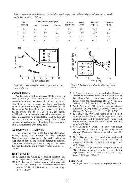
Table 3: Optimized etch characteristics including depth, aspect ratio, sidewall slope, and undercut vs. trench<br />
width. The etch time is 150 min.<br />
Mask<br />
opening<br />
Actual trench width (µm)<br />
Top Middle Bottom<br />
Trench<br />
depth (µm)<br />
Aspect<br />
ratio<br />
Sidewall<br />
slope (⁰)<br />
Undercut<br />
(µm)<br />
2.5 6.3 3 1.7 292 97.3 89.55 1.9<br />
3.5 7.4 3.9 2.5 339 86.9 89.59 1.95<br />
4.4 8.8 4.7 3.4 370 78.7 89.58 2.2<br />
5.3 10 5.7 4.2 398 69.8 89.58 2.35<br />
Aspect ratio<br />
150<br />
100<br />
50<br />
this work<br />
[3]<br />
[6]<br />
[4]<br />
0<br />
0 2 4 6 8 10 12<br />
Trench width (μm)<br />
Figure 6: Aspect ratio of adjusted recipe compared to<br />
state-of-the art.<br />
CONCLUSION<br />
We have developed an advanced DRIE process for<br />
etching ultra high aspect ratio features in silicon. By<br />
ramping the process parameters, including bias power,<br />
step duration, and pressure, we have significantly<br />
increased the achievable aspect ratio for trenches of 1 to<br />
10 µm width. We have shown aspect ratios of 69.8 for a<br />
5.7 µm trench, and up to 97.3 for a 3 µm trench.<br />
Additionally, by ramping the passivation parameters, we<br />
are able to decrease the undercut at the top of the trench to<br />
less than 2 µm for a 5 µm opening. With further<br />
optimization and an improved masking layer, we may be<br />
able to further improve the aspect ratio.<br />
ACKNOWLEDGEMENTS<br />
This work was done in the Lurie Nanofabrication<br />
Facility (LNF), a member of the National<br />
Nanotechnology Infrastructure Network, which is<br />
supported in part by the National Science Foundation.<br />
This project is funded by the MAST Program of the Army<br />
Research Lab (ARL) under Award Number W911NF-08-<br />
2-0004.<br />
REFERENCES<br />
[1] F. Laermer and A. Schilp, “Method of anisotropically<br />
etching silicon,” U.S. Patent 5501893, Mar. 26, 1996.<br />
[2] I. W. Rangelow, “Critical tasks in high aspect ratio<br />
silicon dry etching for microelectromechanical<br />
systems,” J. Vac. Sci. Technol. A, vol. 21, no. 4, pp.<br />
1550-1562, 2003.<br />
Etch rate (μm/min)<br />
4<br />
3<br />
2<br />
2.5μm<br />
1<br />
3.5μm<br />
4.4μm<br />
5.3μm<br />
0<br />
0 50 100 150<br />
Time (min)<br />
Figure 7: Etch rate over time for different trench<br />
widths.<br />
[3] J. Yeom, Y. Wu, J. C. Selby, and M. A. Shannon,<br />
“Maximum achievable aspect ratio in deep reactive<br />
ion etching of silicon due to aspect ratio dependent<br />
transport and the microloading effect,” J. Vac. Sci.<br />
Technol. B, vol. 23, no. 6, pp. 2319-2329, 2005.<br />
[4] W. J. Park, et al., “High aspect ratio via etching<br />
conditions for deep trench of silicon,” Surface and<br />
Coatings Technology, vol. 171, pp. 290-295, 2003.<br />
[5] F. Marty, et al., “Advanced etching of silicon based<br />
on deep reactive ion etching for high aspect ratio<br />
microstructures and three-dimensional micro- and<br />
nanostructures,” Microelectronics Journal, vol. 36,<br />
pp. 673-677, 2005.<br />
[6] C. K. Chung, H. C. Lu and T. H. Jaw, “High aspect<br />
ratio silicon trench fabrication by inductively coupled<br />
plasma,” Microsystem Technologies vol. 6, pp. 106-<br />
108, 2000.<br />
[7] M. A. Blauw, et al., “Advanced time-multiplexed<br />
plasma etching of high aspect ratio silicon<br />
structures,” J. Vac. Sci. Technol. B, vol. 20, pp. 3106-<br />
3110, 2002.<br />
[8] A. Kok, et al., “High aspect ratio deep RIE for novel<br />
3D radiation sensors in high energy physics<br />
applications,” IEEE Nuclear Science Sym. Conf.<br />
Record, 2009, pp. 1623-1627.<br />
CONTACT<br />
*K. Najafi, tel: +1-734-763-6650; najafi@umich.edu<br />
254
![[Sample B: Approval/Signature Sheet]](https://img.yumpu.com/34084789/1/190x245/sample-b-approval-signature-sheet.jpg?quality=85)