A 14 mW Fractional-N PLL Modulator With a Digital ... - IEEE Xplore
A 14 mW Fractional-N PLL Modulator With a Digital ... - IEEE Xplore
A 14 mW Fractional-N PLL Modulator With a Digital ... - IEEE Xplore

Create successful ePaper yourself
Turn your PDF publications into a flip-book with our unique Google optimized e-Paper software.
FERRISS AND FLYNN: A <strong>14</strong> <strong>mW</strong> FRACTIONAL-N <strong>PLL</strong> MODULATOR WITH A DIGITAL PHASE DETECTOR AND FREQUENCY SWITCHING SCHEME 2469<br />
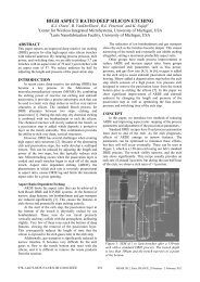
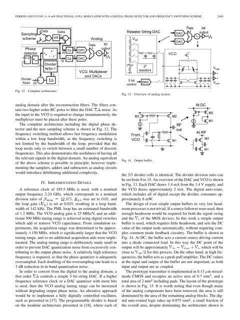
Fig. 12. Complete architecture.<br />
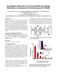
Fig. 13. Overview of analog section.<br />
analog domain after the reconstruction filters. The filters contain<br />
two higher order RC poles to filter the DAC noise. As<br />
the input to the VCO is required to change instantaneously, the<br />
multiplexer must be placed after these poles.<br />
The complete architecture including the digital phase detector<br />
and the new sampling scheme is shown in Fig. 12. The<br />
frequency switching method allows fast frequency modulation<br />
within a low loop bandwidth, as the frequency switching is<br />
not limited by the bandwidth of the loop, provided that the<br />
loop needs only to switch between a small number of discrete<br />
frequencies. This also demonstrates the usefulness of having all<br />
the relevant signals in the digital domain. An analog equivalent<br />
of the above scheme is possible in principle, however implementing<br />
the samplers, adders and subtractors as analog circuits<br />
would introduce debilitating additional complexity.<br />
IV. IMPLEMENTATION DETAILS<br />
A reference clock of 185.5 MHz is used, with a nominal<br />
output frequency 2.24 GHz, which corresponds to a nominal<br />
division ratio of . was set to 0.01, and<br />
the loop gain ( ) is set at 0.025, resulting in a loop bandwidth<br />
of <strong>14</strong>2 kHz. The PML loop has an estimated bandwidth<br />
of 1.2 MHz. The VCO analog gain is 25 MHz/V, and an additional<br />
500 MHz tuning range is achieved using digital switches<br />
which add or remove VCO capacitance. From simulation experiments,<br />
the acquisition range was determined to be approximately<br />
150 MHz, which is significantly larger that the VCO<br />
tuning range, and so no additional acquisition aids were implemented.<br />
The analog tuning range is deliberately made small in<br />
order to prevent DAC quantization noise from excessively contributing<br />
to the output phase noise. A relatively high reference<br />
frequency is required, so that the phase quantizer is adequately<br />
oversampled. Each doubling of the oversampling rate leads to a<br />
3 dB reduction in in-band quantization noise.<br />
In order to convert from the digital to the analog domain, a<br />
first order controls a simple 5 bit string DAC. If a higher<br />
frequency reference clock or a DAC quantizer with more bits<br />
is used, then the VCO analog tuning range can be increased<br />
without degrading output phase noise. An alterative approach<br />
would be to implement a fully digitally controlled oscillator,<br />
such as presented in [17]. The programmable divider is based<br />
on the modular architecture presented in [18], where each of<br />
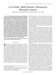
Fig. <strong>14</strong>.<br />
Output buffer.<br />
the 2/3 divider cells is identical. The divider division ratio can<br />
be set from 8 to 15. An overview of the DAC and VCO is shown<br />
in Fig. 13. Each DAC draws 1.4 mA from the 1.4 V supply, and<br />
the VCO draws approximately 2 mA. The digital auto-route,<br />
which includes all of digital except the divider, consumes approximately<br />
6 <strong>mW</strong>.<br />
The design of even simple output buffers in very low headroom<br />
processes is not trivial. If a source follower were used, then<br />
enough headroom would be required for both the signal swing<br />
and the of the MOS devices. In this work a simple output<br />
buffer is used, which requires little headroom, and sets the DC<br />
value of the output node automatically, without requiring complex<br />
common mode feedback circuitry. The buffer is shown in<br />
Fig. <strong>14</strong>. At DC, the buffer acts a current source driving current<br />
into a diode connected load. In this way the DC point of the<br />
output will be approximately<br />
, which will be<br />
close to for this process. On the other hand, at high frequencies,<br />
the buffer acts as a push-pull amplifier. The DC values<br />
at the input and output of the buffer are not important, as both<br />
input and output are ac coupled.<br />
The prototype transmitter is implemented in 0.13 m mixedmode<br />
CMOS and occupies an active area of 0.7 mm , and a<br />
total area of 2 mm including pads. The layout of the prototype<br />
is shown in Fig. 15. It is worth noting that even though many<br />
of the analog components have been removed, the area is still<br />
dominated by the area of the remaining analog blocks. The digital<br />
auto-routed logic takes up 0.075 mm , a small fraction of<br />
the overall area, despite dominating the architecture shown in
![[Sample B: Approval/Signature Sheet]](https://img.yumpu.com/34084789/1/190x245/sample-b-approval-signature-sheet.jpg?quality=85)