Analysis and design of a 200W LDMOS based doherty amplifier for ...
Analysis and design of a 200W LDMOS based doherty amplifier for ...
Analysis and design of a 200W LDMOS based doherty amplifier for ...

You also want an ePaper? Increase the reach of your titles
YUMPU automatically turns print PDFs into web optimized ePapers that Google loves.
e lost when the Doherty <strong>amplifier</strong> is operating below its<br />
transition point. It is there<strong>for</strong>e necessary to add a driver<br />
stage to maximize efficiency. A driver is also added to the<br />
main <strong>amplifier</strong> to accommodate shaping <strong>of</strong> the transfer<br />
characteristics, which is critical in a Doherty <strong>amplifier</strong>.<br />
The splitter asymmetry (A) is set by the gain difference:<br />
A=G,-G, (9)<br />
The gain <strong>of</strong> the total Doherty <strong>amplifier</strong>, at full power, can<br />
then be determined from:<br />
Gm, - 3 +GI - IOlog(l+ (10)<br />
In order to maintain a constant gain over power <strong>for</strong> the<br />
total Doherty <strong>amplifier</strong>, the gain characteristics (AWAM)<br />
<strong>of</strong> the peak <strong>amplifier</strong> should be matched to that <strong>of</strong> the<br />
main <strong>amplifier</strong>, <strong>and</strong>,can be determined from:<br />
G, = 101og(lO"'lo(l+ IOd~~o)-lOG1po)- A (1 1)<br />
The <strong>amplifier</strong>s are <strong>design</strong>ed using internally matched<br />
Philips <strong>LDMOS</strong> transistors. In order to get maximum<br />
efficiency improvement in a Doherty <strong>amplifier</strong> the<br />
transistors need to have specific properties. The transistor<br />
<strong>for</strong> the peak <strong>amplifier</strong> should he <strong>design</strong>ed to have a high<br />
<strong>of</strong>f-state output impedance <strong>and</strong> exhibit low reverse RF<br />
drive. For the main <strong>amplifier</strong> the transistor should he able<br />
to provide maximum per<strong>for</strong>mance under the load pulling<br />
conditions.<br />
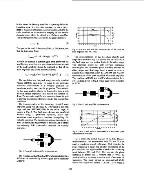
The implementation <strong>of</strong> the two-stage class-AB main<br />
<strong>amplifier</strong>, using two BLF2022-40 (5OWpeak) in the final<br />
stage <strong>and</strong> one BLF2043(10W) in the driver stage, is<br />
shown in Fig. 5. The final stage devices are paralleled<br />
without using a quadrature combiner, since both<br />
transistors must experience in-phase load-pulling <strong>for</strong><br />
Doherty operation. The interstage matching is <strong>design</strong>ed to<br />
meet the b<strong>and</strong>width requirement <strong>of</strong> 60MHz <strong>and</strong> to obtain<br />
approximately 3dB compression required <strong>for</strong> Doherty<br />
operation.<br />
Fig. 5. Class-AB main <strong>amplifier</strong> implementation.<br />
The resulting M AM <strong>and</strong> AMPM characteristics <strong>for</strong> a<br />
50n load are shown in Fig. 6 with a peak power capability<br />
<strong>of</strong> 1oow.<br />
Poldhl<br />
Fig. 6. AM-AM <strong>and</strong> AM-PM characteristics <strong>of</strong> the class-AB<br />
main <strong>amplifier</strong> <strong>for</strong> a 5011 load:<br />
The implementation <strong>of</strong> the two-stage class-C peak<br />
<strong>amplifier</strong> is shown in Fig. 7. It utilizes two BLF2022-40 in<br />
the final stage <strong>and</strong> one similar device in the driver stage.<br />
The interstage circuit not only provides impedance<br />
matching but also the correct phase matching between the<br />
driver output <strong>and</strong> final stage input in order to obtain a<br />
predistortion effect that aligns the M AM <strong>and</strong> AM/PM<br />
characteristics <strong>of</strong> the peak <strong>amplifier</strong> with main <strong>amplifier</strong>.<br />
The resulting M AM <strong>and</strong> AWM characteristics <strong>for</strong> a<br />
50n load are shown in Fig. 8 with a peak power capability<br />
<strong>of</strong> 1oow.<br />
Fig. 7. Class-C peak <strong>amplifier</strong> implementation.<br />
X I I I I I I I -,&a<br />
0 . . . . .. . .. .. . . -155<br />
a11 21 zs a U 24 xi Y U) e " 48 4a a U<br />
hldbl<br />
Fig. 8. AM-AM <strong>and</strong> AM-PM characteristics <strong>of</strong> the class-C peak<br />
<strong>amplifier</strong> <strong>for</strong> a 5On load.<br />
Fig. 9 shows the circuit diagram <strong>of</strong> the total Doberty<br />
implementation. The transmission lines TL3 <strong>and</strong> TL4 are<br />
used to maximize overall efficiency. TL3 provides the<br />
phase matching to rotate the <strong>of</strong>f-state impedance <strong>of</strong> the<br />
peak <strong>amplifier</strong> to a high impedance level at the combining<br />
point between TL5 <strong>and</strong> TL6. TL4 provides the phase<br />
matching to ensure that a resistive load <strong>of</strong> twice the<br />
nominal value is presented at the die level <strong>of</strong> the main PA<br />
transistors. The input utilizes an asymmetrical (5dB)<br />
branch line coupler as a splitter. TLl <strong>and</strong> TJ2 are added to<br />
53 1

![P-CAD EDA - [Sheet1]](https://img.yumpu.com/49470492/1/190x115/p-cad-eda-sheet1.jpg?quality=85)