Issue 19, 2013 - Balliol College - University of Oxford
Issue 19, 2013 - Balliol College - University of Oxford
Issue 19, 2013 - Balliol College - University of Oxford

Create successful ePaper yourself
Turn your PDF publications into a flip-book with our unique Google optimized e-Paper software.
college features<br />
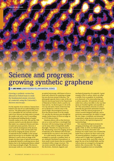
Science and progress:<br />
growing synthetic graphene<br />
By JAmie wArner (JUNIOR RESEARCH FELLOW IN MATERIAL SCIENCE)<br />
Growing a synthetic version has<br />
allowed an <strong>Oxford</strong> team to study<br />
the fundamental atomic structure<br />
<strong>of</strong> a material, using the <strong>University</strong>’s<br />
electron microscope.<br />
For the majority <strong>of</strong> our existence, humans have<br />
looked to the stars for an understanding <strong>of</strong> our<br />
universe. the philosophical aspects that drive<br />
us to contemplate the vast enormity and size<br />
scale <strong>of</strong> our universe also help point us towards<br />
the smaller scale with a view to unravelling<br />
the fundamental building blocks <strong>of</strong> matter.<br />
scientific studies in the early 18th and the <strong>19</strong>th<br />
centuries started to provide physical evidence<br />
that matter was comprised <strong>of</strong> atoms and, later,<br />
revealed sub-atomic particles. However, it<br />
wasn’t until the development <strong>of</strong> the electron<br />
microscope in the <strong>19</strong>30s and thereafter that<br />
the tools for imaging the atomic structure<br />
<strong>of</strong> materials became available. in the normal<br />
optical microscope we are familiar with, light<br />
(photons) is used to form an image <strong>of</strong> the<br />
sample, but these types <strong>of</strong> optical microscopes<br />
are generally limited to resolving micron-sized<br />
features due to the fundamental physics related<br />
to the long wavelength <strong>of</strong> light. the electron<br />
microscope works in a very similar manner to<br />
an optical microscope, with lenses to focus a<br />
beam and a detector for acquiring an image,<br />
but uses electrons instead <strong>of</strong> photons. the<br />
photograph opposite shows a state-<strong>of</strong>-the-art<br />
electron microscope based in the Department<br />
<strong>of</strong> Materials at oxford, which is used by my<br />
team and me. An electron gun (1) sits at the<br />
very top and emits a beam <strong>of</strong> electrons that<br />
are accelerated to a velocity close to the<br />
speed <strong>of</strong> light. electromagnetic lenses (2)<br />
focus the electron beam on to the sample<br />
(3), and after the electrons pass through the<br />
sample, further lenses (4) form an image on<br />
to a CCD detector below.<br />
Quantum physics tells us that electrons<br />
can act as waves and have a wavelength that<br />
decreases with increasing energy and which<br />
can be many orders <strong>of</strong> magnitude smaller<br />
than light. therefore, by using electrons as<br />
the ‘illuminating’ source for imaging, pictures<br />
<strong>of</strong> materials can be obtained with structure<br />
revealed all the way down to the atomic level.<br />
in a solid material, atoms are typically<br />
arranged in a periodic crystalline stack, or<br />
are randomly distributed (amorphous), or<br />
form small crystal clusters that are randomly<br />
orientated within a larger structure. the<br />
way atoms assemble strongly influences<br />
the electronic, chemical, magnetic and<br />
mechanical properties <strong>of</strong> a material. A great<br />
example <strong>of</strong> this is carbon, which can adopt<br />
a metallic form as graphite, be insulating<br />
as in diamond, or be semiconducting as in<br />
a carbon nanotube. All materials are made<br />
solely from carbon, but differ in the way their<br />
atoms are bonded together and assemble in<br />
3D. this extraordinary diversity <strong>of</strong> carbon<br />
materials has generated substantial research<br />
interest. With the natural progression <strong>of</strong><br />
science towards designed materials, and in<br />
particular nanomaterials, the ability to image<br />
the size, shape, crystallinity and elemental<br />
composition, using electron microscopy, has<br />
been critical to the rapid development <strong>of</strong><br />
nanotechnology.<br />
new materials hold great promises for<br />
changing technology and consequently<br />
quality <strong>of</strong> life. in 2010, two British physicists<br />
(Pr<strong>of</strong>essor sir Kostya novoselov and<br />
Pr<strong>of</strong>essor sir Andre Geim) were awarded the<br />
nobel Prize in physics for their work on the<br />
2D material graphene. Graphene is made <strong>of</strong><br />
carbon and is a single sheet <strong>of</strong> graphite. it<br />
is only one atom thick, much like a sheet <strong>of</strong><br />
paper the size <strong>of</strong> ten football fields, and the<br />
carbon atoms are arranged in a hexagonal<br />
pattern, like a honeycomb. the charge<br />
carriers in graphene move at remarkable<br />
20<br />
FLoReAt DoMus BALLioL CoLLeGe neWs