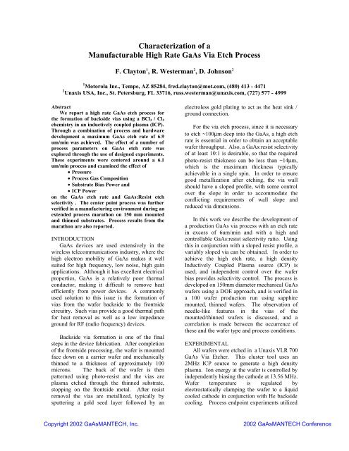
Characterization of a Manufacturable High Rate GaAs ... - CS Mantech
Characterization of a Manufacturable High Rate GaAs ... - CS Mantech
Characterization of a Manufacturable High Rate GaAs ... - CS Mantech

You also want an ePaper? Increase the reach of your titles
YUMPU automatically turns print PDFs into web optimized ePapers that Google loves.
<strong>Characterization</strong> <strong>of</strong> a<br />
<strong>Manufacturable</strong> <strong>High</strong> <strong>Rate</strong> <strong>GaAs</strong> Via Etch Process<br />
F. Clayton 1 , R. Westerman 2 , D. Johnson 2<br />
1 Motorola Inc., Tempe, AZ 85284, fred.clayton@mot.com, (480) 413 - 4471<br />
2 Unaxis USA, Inc., St. Petersburg, FL 33716, russ.westerman@unaxis.com, (727) 577 - 4999<br />
Abstract<br />
We report a high rate <strong>GaAs</strong> etch process for<br />
the formation <strong>of</strong> backside vias using a BCl 3 / Cl 2<br />
chemistry in an inductively coupled plasma (ICP).<br />
Through a combination <strong>of</strong> process and hardware<br />
development a maximum <strong>GaAs</strong> etch rate <strong>of</strong> 6.9<br />
um/min was achieved. The effect <strong>of</strong> a number <strong>of</strong><br />
process parameters on <strong>GaAs</strong> etch rate was<br />
explored through the use <strong>of</strong> designed experiments.<br />
These experiments were centered around a 6.1<br />
um/min process and examined the effect <strong>of</strong><br />
• Pressure<br />
• Process Gas Composition<br />
• Substrate Bias Power and<br />
• ICP Power<br />
on the <strong>GaAs</strong> etch rate and <strong>GaAs</strong>:Resist etch<br />
selectivity . The center point process was further<br />
verified in a manufacturing environment during an<br />
extended process marathon on 150 mm mounted<br />
and thinned substrates. Process results from the<br />
marathon are also reported.<br />
INTRODUCTION<br />
<strong>GaAs</strong> devices are used extensively in the<br />
wireless telecommunications industry, where the<br />
high electron mobility <strong>of</strong> <strong>GaAs</strong> makes it well<br />
suited for high frequency, low noise, high gain<br />
applications. Although it has excellent electrical<br />
properties, <strong>GaAs</strong> is a relatively poor thermal<br />
conductor, making it difficult to remove heat<br />
efficiently from power devices. A commonly<br />
used solution to this issue is the formation <strong>of</strong><br />
vias from the wafer backside to the frontside<br />
circuitry. Such vias provide a good thermal path<br />
for heat removal as well as a low impedance<br />
ground for RF (radio frequency) devices.<br />
Backside via formation is one <strong>of</strong> the final<br />
steps in the device fabrication. After completion<br />
<strong>of</strong> the frontside processing, the wafer is mounted<br />
face down on a carrier wafer and mechanically<br />
thinned to a thickness <strong>of</strong> approximately 100<br />
microns. The back <strong>of</strong> the wafer is then<br />
patterned using photo-resist and the vias are<br />
plasma etched through the thinned substrate,<br />
stopping on the frontside metal. After resist<br />
removal the vias are metallized, typically by<br />
sputtering a gold seed layer followed by an<br />
electroless gold plating to act as the heat sink /<br />
ground connection.<br />
For the via etch process, since it is necessary<br />
to etch ~100µm deep into the <strong>GaAs</strong>, a high etch<br />
rate is essential in order to obtain an acceptable<br />
wafer throughput. Also, a <strong>GaAs</strong>:resist selectivity<br />
<strong>of</strong> at least 10:1 is desirable, so that the required<br />
photo-resist thickness can be less than ~14µm,<br />
which is the maximum thickness typically<br />
achievable in a single spin. In order to ensure<br />
good metallization after etching, the via wall<br />
should have a sloped pr<strong>of</strong>ile, with some control<br />
over the slope in order to accommodate the<br />
conflicting requirements <strong>of</strong> wall slope and<br />
reduced via dimensions.<br />
In this work we describe the development <strong>of</strong><br />
a production <strong>GaAs</strong> via process with an etch rate<br />
in excess <strong>of</strong> 6um/min and with a high and<br />
controllable <strong>GaAs</strong>:resist selectivity ratio. Using<br />
this in conjunction with a sloped resist pr<strong>of</strong>ile, a<br />
variably sloped via can be obtained. In order to<br />
achieve the high etch rate, a high density<br />
Inductively Coupled Plasma source (ICP) is<br />
used, and independent control over the wafer<br />
bias provides selectivity control. The process is<br />
developed on 150mm diameter mechanical <strong>GaAs</strong><br />
wafers using a DOE approach, and is verified in<br />
a 100 wafer production run using sapphire<br />
mounted, thinned wafers. The observation <strong>of</strong><br />
needle-like features in the vias <strong>of</strong> the<br />
mounted/thinned wafers is discussed, and a<br />
correlation is made between the occurrence <strong>of</strong><br />
these and the wafer type and process conditions.<br />
EXPERIMENTAL<br />
All wafers were etched in a Unaxis VLR 700<br />
<strong>GaAs</strong> Via Etcher. This cluster tool uses an<br />
2MHz ICP source to generate a high density<br />
plasma. Ion energy at the wafer is controlled by<br />
independently biasing the cathode at 13.56 MHz.<br />
Wafer temperature is regulated by<br />
electrostatically clamping the wafer to a liquid<br />
cooled cathode in conjunction with He backside<br />
cooling. Process endpoint experiments utilized
<strong>GaAs</strong> Via Wall Angle<br />
(degrees)<br />
a Unaxis Spectraworks optical emission system<br />
(OES).<br />
The substrates used in these experiments<br />
were 150 mm <strong>GaAs</strong> wafers patterned with a<br />
photoresist mask. The total exposed area <strong>of</strong> the<br />
test pattern was approximately 15% - a large<br />
portion <strong>of</strong> that area was due to a 3 mm<br />
photoresist edge bead removal required later in<br />
the process flow (exposed via area was 7%).<br />
Initial process development was performed on<br />
mechanical wafers while the final process<br />
verification utilized sapphire mounted, thinned<br />
slices which included a frontside metal etch stop.<br />
All depth measurements were performed<br />
using a step pr<strong>of</strong>ilometer. Mechanical <strong>GaAs</strong><br />
samples were partially etched while the thinned,<br />
mounted samples were etched to completion.<br />
RESULTS AND DISCUSSION<br />
Plasma etch processes for <strong>GaAs</strong> typically<br />
utilize a chlorine-based chemistry. Though a Cl 2<br />
plasma alone is sufficient to etch <strong>GaAs</strong>,<br />
additional reactants are <strong>of</strong>ten added to obtain a<br />
clean anisotropic etch. The goal <strong>of</strong> this work<br />
was to double the <strong>GaAs</strong> etch rate (from 3<br />
um/min to 6 um/min) for a production qualified<br />
BCl 3 / Cl 2 process 1,2 without perturbing<br />
downstream manufacturability.<br />
90<br />
75<br />
60<br />
45<br />
30<br />
15<br />
0<br />
<strong>GaAs</strong> Via Wall Slope vs. Photoresist Slope<br />
(at various <strong>GaAs</strong>:PR selectivities)<br />
32<br />
16<br />
8<br />
Selectivity<br />
(<strong>GaAs</strong>:PR)<br />
4<br />
2<br />
1<br />
<strong>GaAs</strong><br />
Resist<br />
0 15 30 45 60 75 90<br />
PR Wall Angle<br />
(degrees)<br />
Figure 1. Expected <strong>GaAs</strong> via pr<strong>of</strong>ile as a function <strong>of</strong><br />
resist slope and <strong>GaAs</strong>:resist etch selectivity<br />
<strong>GaAs</strong>:Resist etch selectivity. This approach<br />
allows the initial resist pr<strong>of</strong>ile to be “driven” into<br />
the via. Figure 1 shows a model <strong>of</strong> the<br />
relationship between the initial resist pr<strong>of</strong>ile and<br />
the expected <strong>GaAs</strong> via pr<strong>of</strong>ile as a function <strong>of</strong><br />
<strong>GaAs</strong>:Resist etch selectivity. The base line<br />
process prior to this work used this approach to<br />
achieve a sloped via. In order to minimize any<br />
impact on downstream operations (specifically<br />
metallization), it was important to maintain the<br />
baseline <strong>GaAs</strong>:Resist etch selectivity in order to<br />
maintain the baseline via pr<strong>of</strong>ile.<br />
Both hardware and process changes were<br />
required to achieve the 6 µm/min <strong>GaAs</strong> etch rate<br />
goal. Preliminary experiments showed that the<br />
<strong>GaAs</strong> rate increased with increased Cl 2 flows,<br />
requiring resizing <strong>of</strong> the MFCs. Further etch rate<br />
enhancements were achieved through<br />
modifications to the ICP source.<br />
A designed experiment (DOE) was<br />
performed to map out the process space. While<br />
factorial experiments are a reliable way to map<br />
process responses, they quickly become cost<br />
prohibitive for a larger number <strong>of</strong> factors.<br />
Fractional factorial experiments are a convenient<br />
way to map factor responses, balancing time and<br />
material requirements with the quality <strong>of</strong> the<br />
calculated responses.<br />
A four factor half fractional (2 4-1 ) design was<br />
chosen to explore the process window. This<br />
design explores the process space <strong>of</strong> 4 factors in<br />
only 11 experiments (8 + 3 centerpoint repeats)<br />
but is unable to resolve two factor interactions.<br />
If a two factor interaction is indicated in the<br />
statistical analysis, further experiments would be<br />
required to isolate the interaction. No significant<br />
Design Layout<br />
Factor Name Low <strong>High</strong><br />
Pressure mtorr 14 18<br />
ICP W 800 1200<br />
RIE W 115 155<br />
% Cl 2 % 80 90<br />
While an anisotropic etch pr<strong>of</strong>ile <strong>of</strong>fers the<br />
best CD control, practically it is difficult to<br />
metallize. In order to lower the aspect ratio for<br />
ease <strong>of</strong> metallization, a sloped via pr<strong>of</strong>ile is<br />
preferred. One approach to obtain a sloped via<br />
pr<strong>of</strong>ile is through a combination <strong>of</strong> a sloped<br />
initial photoresist pr<strong>of</strong>ile and controllable<br />
Responses<br />
<strong>GaAs</strong> <strong>Rate</strong><br />
Select<br />
PR <strong>Rate</strong><br />
DC Bias<br />
RIE<br />
Composition<br />
Pressure<br />
Low<br />
Figure 2. Summary <strong>of</strong> Designed Experiment. Range <strong>of</strong><br />
factors explored and schematic <strong>of</strong> 2 4-1 design<br />
ICP<br />
RIE<br />
Composition<br />
Pressure<br />
<strong>High</strong><br />
ICP
two factor interactions were found during the<br />
analysis <strong>of</strong> these designs.<br />
18<br />
Overlay Plot<br />
The design examined the effects <strong>of</strong> four<br />
factors (pressure, ICP power, bias power, and<br />
reactant gas composition) on three responses<br />
(<strong>GaAs</strong> etch rate, resist etch rate, and <strong>GaAs</strong>:Resist<br />
etch selectivity). Process temperature, total gas<br />
flow, etch time and the hardware configuration<br />
were all held constant throughout the design.<br />
Figure 2 shows the range <strong>of</strong> factors explored<br />
along with a schematic <strong>of</strong> the half fractional<br />
design. A post etch inspection <strong>of</strong> the wafers was<br />
performed using an optical microscope to check<br />
etch morphology. All cells <strong>of</strong> the DOE exhibited<br />
clean, smooth etched surfaces. Following<br />
inspection, the wafers were stripped and<br />
measured. Figure 3 summarizes the DOE<br />
trends. The <strong>GaAs</strong> removal rate appears<br />
chemically driven – the <strong>GaAs</strong> etch rate increases<br />
with pressure, ICP power and increased Cl 2<br />
fraction. Resist removal in a BCl 3 / Cl 2<br />
chemistry appears physically driven – the resist<br />
etch rate increased solely with the RF bias<br />
power.<br />
Factor<br />
<strong>GaAs</strong><br />
<strong>Rate</strong><br />
Response<br />
Resist<br />
<strong>Rate</strong><br />
<strong>GaAs</strong>:Resist<br />
Selectivity<br />
↑ Pressure ↑ ↑<br />
↑ ICP<br />
↑<br />
↑ RF Bias ↑ ↓<br />
↑ % Cl 2<br />
↑<br />
Pressure<br />
17<br />
16<br />
15<br />
<strong>GaAs</strong> <strong>Rate</strong> > 6.0<br />
14<br />
800 900 1000 1100 1200<br />
ICP<br />
Figure 4. Process space as a function <strong>of</strong> process<br />
pressure and ICP power<br />
In order to qualify the process for release to<br />
manufacturing, a 100 wafer etch marathon test<br />
was performed. The 100 wafer sample set was<br />
comprised <strong>of</strong> substrates from four different<br />
vendors. The wafers were metallized, mounted,<br />
thinned and patterned using identical processes.<br />
After patterning, the wafers were etched to full<br />
depth using the centerpoint process from the<br />
designed experiment. Etch end point was<br />
detected by monitoring the 417nm Ga line by<br />
OES. After every 10th mounted wafer was<br />
etched, a mechanical wafer was partially etched<br />
(10 minutes) to monitor etch rate and selectivity.<br />
(Figure 5) The mechanical etch monitors ranged<br />
3<br />
Select > 9.5:1<br />
Figure 3. Response trends from Designed Experiment<br />
The <strong>GaAs</strong>:Resist etch selectivity was found<br />
to be a function <strong>of</strong> both pressure and RF bias<br />
power. It is important to note that while the<br />
<strong>GaAs</strong>:Resist selectivity is a strong function RF<br />
bias power, the <strong>GaAs</strong> etch rate is bias power<br />
independent. Since the final via pr<strong>of</strong>ile is a<br />
strong function <strong>of</strong> <strong>GaAs</strong>:Resist selectivity<br />
(Figure 1), the RF bias power can be used to<br />
adjust the final via pr<strong>of</strong>ile independent <strong>of</strong> the<br />
<strong>GaAs</strong> etch rate. Figure 4 maps the process<br />
space as a function <strong>of</strong> ICP power and pressure<br />
where the <strong>GaAs</strong> rate is greater than 6 µm/min<br />
and the <strong>GaAs</strong>:Resist selectivity is greater than<br />
9.5:1.<br />
<strong>GaAs</strong> Etch <strong>Rate</strong><br />
<br />
8<br />
6<br />
4<br />
2<br />
Etch <strong>Rate</strong> vs Wafer Number<br />
6" Mounted / Thinned <strong>GaAs</strong><br />
0<br />
0 10 20 30 40 50 60 70 80 90 100<br />
Wafer<br />
Figure 5. <strong>GaAs</strong> etch rate from 100 wafer process<br />
marathon. Etch rate measured on partially etched<br />
mechanical <strong>GaAs</strong> wafers
Figure 6. SEM cross section <strong>of</strong> via with and without grass<br />
formation. Note sloped pr<strong>of</strong>ile<br />
from 5.6 to 6.6 µm/min during the course <strong>of</strong> the<br />
process marathon.<br />
A post etch inspection <strong>of</strong> the marathon<br />
wafers was performed using an optical<br />
microscope to check etch morphology. Sparse<br />
grass was present in a fraction <strong>of</strong> the vias on a<br />
number <strong>of</strong> wafers (Figure 6). The formation <strong>of</strong><br />
grass during via etching has been previously<br />
reported in the literature by Nam et al. 3 In order<br />
to quantify the extent <strong>of</strong> grass formation, data<br />
was collected from 15 vias on each <strong>of</strong> 7 sites in a<br />
diagonal pattern on each wafer counted. Four<br />
wafers from each vendor representing a<br />
minimum <strong>of</strong> 3 boules per vendor were analyzed.<br />
Each via was binned according the number <strong>of</strong><br />
pillar-like grass structures present in the via.<br />
Figure 7 shows the correlation between the<br />
material supplier and pillar formation. Material<br />
D exhibited an areal density <strong>of</strong> 0.51 pillars/mm 2<br />
with 80% grass free vias, while material A had<br />
an areal density <strong>of</strong> 6.03 pillars/mm 2 with only<br />
10% <strong>of</strong> the vias pillar free. Further reductions in<br />
pillar density were achieved through additional<br />
process development using the worst case<br />
material (Material A).<br />
CONCLUSIONS<br />
A 75% improvement in via etch throughput<br />
was achieved by a combination <strong>of</strong> process and<br />
hardware developments. The <strong>GaAs</strong> etch rate <strong>of</strong> a<br />
production proven 150 mm <strong>GaAs</strong> via etch<br />
process was doubled from 3 µm/min to 6<br />
µm/min with minimal impact on downstream<br />
processes. Using a sloped resist mask, sloped<br />
via pr<strong>of</strong>iles are achieved through resist erosion at<br />
reduced (11:1) <strong>GaAs</strong>:Resist selectivities.<br />
Designed experiments show that the RF bias<br />
power can be used to control the final via pr<strong>of</strong>ile<br />
independently <strong>of</strong> the <strong>GaAs</strong> etch rate. Sparse<br />
grass formation seen in some design cells was<br />
influenced by material supplier as well as<br />
process conditions. Etch endpoint detection has<br />
been demonstrated through monitoring the 417<br />
nm Ga line by optical emission spectroscopy<br />
(OES).<br />
ACKNOWLEDGEMENTS<br />
We wish to thank Mike DeVre, Dirk<br />
Bottesch, Carolina Rios Wasson, and Bill<br />
Martinez for their technical and manufacturing<br />
contributions. We would also like to thank Scott<br />
Klingbeil for his support <strong>of</strong> this work.<br />
Figure 7. Pillar formation as a function <strong>of</strong> substrate<br />
supplier. Material D shows 80% pillar free vias. Material A<br />
shows 10% pillar free vias.<br />
[1] Adams KM, Klingbeil LS, 2000 <strong>GaAs</strong> MANTECH<br />
Technical Digest, pp. 75–78.<br />
[2] Klingbeil LS, Kirschenbaum KL, Rampley CG, Young<br />
D, 2001 <strong>GaAs</strong> MANTECH Technical Digest, pp. 41-44.<br />
[3] Nam PS, Ferreira LM, Lee TY, Tu KN, J. Vac. Sci.<br />
Technol. B 18(6), pp. 2780-2784 (2000).