Characterization of a Manufacturable High Rate GaAs ... - CS Mantech
Characterization of a Manufacturable High Rate GaAs ... - CS Mantech
Characterization of a Manufacturable High Rate GaAs ... - CS Mantech

Create successful ePaper yourself
Turn your PDF publications into a flip-book with our unique Google optimized e-Paper software.
<strong>GaAs</strong> Via Wall Angle<br />
(degrees)<br />
a Unaxis Spectraworks optical emission system<br />
(OES).<br />
The substrates used in these experiments<br />
were 150 mm <strong>GaAs</strong> wafers patterned with a<br />
photoresist mask. The total exposed area <strong>of</strong> the<br />
test pattern was approximately 15% - a large<br />
portion <strong>of</strong> that area was due to a 3 mm<br />
photoresist edge bead removal required later in<br />
the process flow (exposed via area was 7%).<br />
Initial process development was performed on<br />
mechanical wafers while the final process<br />
verification utilized sapphire mounted, thinned<br />
slices which included a frontside metal etch stop.<br />
All depth measurements were performed<br />
using a step pr<strong>of</strong>ilometer. Mechanical <strong>GaAs</strong><br />
samples were partially etched while the thinned,<br />
mounted samples were etched to completion.<br />
RESULTS AND DISCUSSION<br />
Plasma etch processes for <strong>GaAs</strong> typically<br />
utilize a chlorine-based chemistry. Though a Cl 2<br />
plasma alone is sufficient to etch <strong>GaAs</strong>,<br />
additional reactants are <strong>of</strong>ten added to obtain a<br />
clean anisotropic etch. The goal <strong>of</strong> this work<br />
was to double the <strong>GaAs</strong> etch rate (from 3<br />
um/min to 6 um/min) for a production qualified<br />
BCl 3 / Cl 2 process 1,2 without perturbing<br />
downstream manufacturability.<br />
90<br />
75<br />
60<br />
45<br />
30<br />
15<br />
0<br />
<strong>GaAs</strong> Via Wall Slope vs. Photoresist Slope<br />
(at various <strong>GaAs</strong>:PR selectivities)<br />
32<br />
16<br />
8<br />
Selectivity<br />
(<strong>GaAs</strong>:PR)<br />
4<br />
2<br />
1<br />
<strong>GaAs</strong><br />
Resist<br />
0 15 30 45 60 75 90<br />
PR Wall Angle<br />
(degrees)<br />
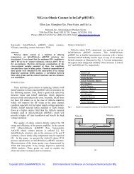
Figure 1. Expected <strong>GaAs</strong> via pr<strong>of</strong>ile as a function <strong>of</strong><br />
resist slope and <strong>GaAs</strong>:resist etch selectivity<br />
<strong>GaAs</strong>:Resist etch selectivity. This approach<br />
allows the initial resist pr<strong>of</strong>ile to be “driven” into<br />
the via. Figure 1 shows a model <strong>of</strong> the<br />
relationship between the initial resist pr<strong>of</strong>ile and<br />
the expected <strong>GaAs</strong> via pr<strong>of</strong>ile as a function <strong>of</strong><br />
<strong>GaAs</strong>:Resist etch selectivity. The base line<br />
process prior to this work used this approach to<br />
achieve a sloped via. In order to minimize any<br />
impact on downstream operations (specifically<br />
metallization), it was important to maintain the<br />
baseline <strong>GaAs</strong>:Resist etch selectivity in order to<br />
maintain the baseline via pr<strong>of</strong>ile.<br />
Both hardware and process changes were<br />
required to achieve the 6 µm/min <strong>GaAs</strong> etch rate<br />
goal. Preliminary experiments showed that the<br />
<strong>GaAs</strong> rate increased with increased Cl 2 flows,<br />
requiring resizing <strong>of</strong> the MFCs. Further etch rate<br />
enhancements were achieved through<br />
modifications to the ICP source.<br />
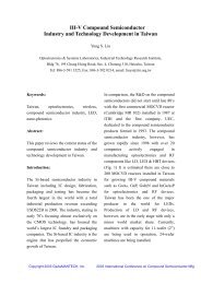
A designed experiment (DOE) was<br />
performed to map out the process space. While<br />
factorial experiments are a reliable way to map<br />
process responses, they quickly become cost<br />
prohibitive for a larger number <strong>of</strong> factors.<br />
Fractional factorial experiments are a convenient<br />
way to map factor responses, balancing time and<br />
material requirements with the quality <strong>of</strong> the<br />
calculated responses.<br />
A four factor half fractional (2 4-1 ) design was<br />
chosen to explore the process window. This<br />
design explores the process space <strong>of</strong> 4 factors in<br />
only 11 experiments (8 + 3 centerpoint repeats)<br />
but is unable to resolve two factor interactions.<br />
If a two factor interaction is indicated in the<br />
statistical analysis, further experiments would be<br />
required to isolate the interaction. No significant<br />
Design Layout<br />
Factor Name Low <strong>High</strong><br />
Pressure mtorr 14 18<br />
ICP W 800 1200<br />
RIE W 115 155<br />
% Cl 2 % 80 90<br />
While an anisotropic etch pr<strong>of</strong>ile <strong>of</strong>fers the<br />
best CD control, practically it is difficult to<br />
metallize. In order to lower the aspect ratio for<br />
ease <strong>of</strong> metallization, a sloped via pr<strong>of</strong>ile is<br />
preferred. One approach to obtain a sloped via<br />
pr<strong>of</strong>ile is through a combination <strong>of</strong> a sloped<br />
initial photoresist pr<strong>of</strong>ile and controllable<br />
Responses<br />
<strong>GaAs</strong> <strong>Rate</strong><br />
Select<br />
PR <strong>Rate</strong><br />
DC Bias<br />
RIE<br />
Composition<br />
Pressure<br />
Low<br />
Figure 2. Summary <strong>of</strong> Designed Experiment. Range <strong>of</strong><br />
factors explored and schematic <strong>of</strong> 2 4-1 design<br />
ICP<br />
RIE<br />
Composition<br />
Pressure<br />
<strong>High</strong><br />
ICP