Characterization of a Manufacturable High Rate GaAs ... - CS Mantech
Characterization of a Manufacturable High Rate GaAs ... - CS Mantech
Characterization of a Manufacturable High Rate GaAs ... - CS Mantech

Create successful ePaper yourself
Turn your PDF publications into a flip-book with our unique Google optimized e-Paper software.
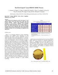
two factor interactions were found during the<br />
analysis <strong>of</strong> these designs.<br />
18<br />
Overlay Plot<br />
The design examined the effects <strong>of</strong> four<br />
factors (pressure, ICP power, bias power, and<br />
reactant gas composition) on three responses<br />
(<strong>GaAs</strong> etch rate, resist etch rate, and <strong>GaAs</strong>:Resist<br />
etch selectivity). Process temperature, total gas<br />
flow, etch time and the hardware configuration<br />
were all held constant throughout the design.<br />
Figure 2 shows the range <strong>of</strong> factors explored<br />
along with a schematic <strong>of</strong> the half fractional<br />
design. A post etch inspection <strong>of</strong> the wafers was<br />
performed using an optical microscope to check<br />
etch morphology. All cells <strong>of</strong> the DOE exhibited<br />
clean, smooth etched surfaces. Following<br />
inspection, the wafers were stripped and<br />
measured. Figure 3 summarizes the DOE<br />
trends. The <strong>GaAs</strong> removal rate appears<br />
chemically driven – the <strong>GaAs</strong> etch rate increases<br />
with pressure, ICP power and increased Cl 2<br />
fraction. Resist removal in a BCl 3 / Cl 2<br />
chemistry appears physically driven – the resist<br />
etch rate increased solely with the RF bias<br />
power.<br />
Factor<br />
<strong>GaAs</strong><br />
<strong>Rate</strong><br />
Response<br />
Resist<br />
<strong>Rate</strong><br />
<strong>GaAs</strong>:Resist<br />
Selectivity<br />
↑ Pressure ↑ ↑<br />
↑ ICP<br />
↑<br />
↑ RF Bias ↑ ↓<br />
↑ % Cl 2<br />
↑<br />
Pressure<br />
17<br />
16<br />
15<br />
<strong>GaAs</strong> <strong>Rate</strong> > 6.0<br />
14<br />
800 900 1000 1100 1200<br />
ICP<br />
Figure 4. Process space as a function <strong>of</strong> process<br />
pressure and ICP power<br />
In order to qualify the process for release to<br />
manufacturing, a 100 wafer etch marathon test<br />
was performed. The 100 wafer sample set was<br />
comprised <strong>of</strong> substrates from four different<br />
vendors. The wafers were metallized, mounted,<br />
thinned and patterned using identical processes.<br />
After patterning, the wafers were etched to full<br />
depth using the centerpoint process from the<br />
designed experiment. Etch end point was<br />
detected by monitoring the 417nm Ga line by<br />
OES. After every 10th mounted wafer was<br />
etched, a mechanical wafer was partially etched<br />
(10 minutes) to monitor etch rate and selectivity.<br />
(Figure 5) The mechanical etch monitors ranged<br />
3<br />
Select > 9.5:1<br />
Figure 3. Response trends from Designed Experiment<br />
The <strong>GaAs</strong>:Resist etch selectivity was found<br />
to be a function <strong>of</strong> both pressure and RF bias<br />
power. It is important to note that while the<br />
<strong>GaAs</strong>:Resist selectivity is a strong function RF<br />
bias power, the <strong>GaAs</strong> etch rate is bias power<br />
independent. Since the final via pr<strong>of</strong>ile is a<br />
strong function <strong>of</strong> <strong>GaAs</strong>:Resist selectivity<br />
(Figure 1), the RF bias power can be used to<br />
adjust the final via pr<strong>of</strong>ile independent <strong>of</strong> the<br />
<strong>GaAs</strong> etch rate. Figure 4 maps the process<br />
space as a function <strong>of</strong> ICP power and pressure<br />
where the <strong>GaAs</strong> rate is greater than 6 µm/min<br />
and the <strong>GaAs</strong>:Resist selectivity is greater than<br />
9.5:1.<br />
<strong>GaAs</strong> Etch <strong>Rate</strong><br />
<br />
8<br />
6<br />
4<br />
2<br />
Etch <strong>Rate</strong> vs Wafer Number<br />
6" Mounted / Thinned <strong>GaAs</strong><br />
0<br />
0 10 20 30 40 50 60 70 80 90 100<br />
Wafer<br />
Figure 5. <strong>GaAs</strong> etch rate from 100 wafer process<br />
marathon. Etch rate measured on partially etched<br />
mechanical <strong>GaAs</strong> wafers