Characterization of a Manufacturable High Rate GaAs ... - CS Mantech
Characterization of a Manufacturable High Rate GaAs ... - CS Mantech
Characterization of a Manufacturable High Rate GaAs ... - CS Mantech

You also want an ePaper? Increase the reach of your titles
YUMPU automatically turns print PDFs into web optimized ePapers that Google loves.
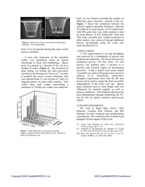
Figure 6. SEM cross section <strong>of</strong> via with and without grass<br />
formation. Note sloped pr<strong>of</strong>ile<br />
from 5.6 to 6.6 µm/min during the course <strong>of</strong> the<br />
process marathon.<br />
A post etch inspection <strong>of</strong> the marathon<br />
wafers was performed using an optical<br />
microscope to check etch morphology. Sparse<br />
grass was present in a fraction <strong>of</strong> the vias on a<br />
number <strong>of</strong> wafers (Figure 6). The formation <strong>of</strong><br />
grass during via etching has been previously<br />
reported in the literature by Nam et al. 3 In order<br />
to quantify the extent <strong>of</strong> grass formation, data<br />
was collected from 15 vias on each <strong>of</strong> 7 sites in a<br />
diagonal pattern on each wafer counted. Four<br />
wafers from each vendor representing a<br />
minimum <strong>of</strong> 3 boules per vendor were analyzed.<br />
Each via was binned according the number <strong>of</strong><br />
pillar-like grass structures present in the via.<br />
Figure 7 shows the correlation between the<br />
material supplier and pillar formation. Material<br />
D exhibited an areal density <strong>of</strong> 0.51 pillars/mm 2<br />
with 80% grass free vias, while material A had<br />
an areal density <strong>of</strong> 6.03 pillars/mm 2 with only<br />
10% <strong>of</strong> the vias pillar free. Further reductions in<br />
pillar density were achieved through additional<br />
process development using the worst case<br />
material (Material A).<br />
CONCLUSIONS<br />
A 75% improvement in via etch throughput<br />
was achieved by a combination <strong>of</strong> process and<br />
hardware developments. The <strong>GaAs</strong> etch rate <strong>of</strong> a<br />
production proven 150 mm <strong>GaAs</strong> via etch<br />
process was doubled from 3 µm/min to 6<br />
µm/min with minimal impact on downstream<br />
processes. Using a sloped resist mask, sloped<br />
via pr<strong>of</strong>iles are achieved through resist erosion at<br />
reduced (11:1) <strong>GaAs</strong>:Resist selectivities.<br />
Designed experiments show that the RF bias<br />
power can be used to control the final via pr<strong>of</strong>ile<br />
independently <strong>of</strong> the <strong>GaAs</strong> etch rate. Sparse<br />
grass formation seen in some design cells was<br />
influenced by material supplier as well as<br />
process conditions. Etch endpoint detection has<br />
been demonstrated through monitoring the 417<br />
nm Ga line by optical emission spectroscopy<br />
(OES).<br />
ACKNOWLEDGEMENTS<br />
We wish to thank Mike DeVre, Dirk<br />
Bottesch, Carolina Rios Wasson, and Bill<br />
Martinez for their technical and manufacturing<br />
contributions. We would also like to thank Scott<br />
Klingbeil for his support <strong>of</strong> this work.<br />
Figure 7. Pillar formation as a function <strong>of</strong> substrate<br />
supplier. Material D shows 80% pillar free vias. Material A<br />
shows 10% pillar free vias.<br />
[1] Adams KM, Klingbeil LS, 2000 <strong>GaAs</strong> MANTECH<br />
Technical Digest, pp. 75–78.<br />
[2] Klingbeil LS, Kirschenbaum KL, Rampley CG, Young<br />
D, 2001 <strong>GaAs</strong> MANTECH Technical Digest, pp. 41-44.<br />
[3] Nam PS, Ferreira LM, Lee TY, Tu KN, J. Vac. Sci.<br />
Technol. B 18(6), pp. 2780-2784 (2000).