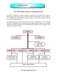
presentation - eufanet
presentation - eufanet
presentation - eufanet

You also want an ePaper? Increase the reach of your titles
YUMPU automatically turns print PDFs into web optimized ePapers that Google loves.
4 October 2006<br />
Addressing the Challenge of Backside<br />
Circuit Edit of Wafer-Level Packages<br />
by T Lundquist, D Di Donato, T Malik<br />
ESREF-EuFANet 2006, Wuppertal, Germany
Motivation:<br />
• Die down PCB attachment is the trend<br />
– Reduces cost (decreases process steps)<br />
– No package—die is the package WL-CSP<br />
– PCB real estate valuable—smaller is better everywhere<br />
• < 40% of WL-CSP die accessible<br />
– FS-CE restricted by 1) balls/pads, 2) redistribution layer<br />
(RDL), 3) protective & passivation layers<br />
– Backside CE<br />
Die Size Balls<br />
(mm) in Array<br />
1 x 1 2 x 2<br />
2 x 2 4 x 4<br />
3 x 3 6 x 6<br />
Wafer Level-Chip Scale Package<br />
from Future Fab website<br />
2 ESREF-EuFANet 2006, Wuppertal, Germany
from 3 Fujiwara Website<br />
ESREF-EuFANet 2006, Wuppertal, Germany
When FS CE not doable then BS CE<br />
• Solder attaches die to PCB<br />
– Die stable to handle PCB warpage, etc<br />
– Strength & thinness of “die” important<br />
• For BS CE, die thinned (100-30μm); standard process<br />
– Mirror-like surface finish needed for trenching<br />
• Use “crystal bond” to mount die<br />
• WL-CSP difficult to handle, not for BS CE but for post edit functionality<br />
– Issue when die to be installed into PCB:<br />
– Remove from mount, die “rolls up”<br />
• Requirement: Structural strength must be re-established<br />
4 ESREF-EuFANet 2006, Wuppertal, Germany
Backside Die Thinning<br />
Die sitting on thinning<br />
puck ready to be<br />
mounted onto puck<br />
Die being mounted with<br />
“crystal bond”<br />
Die thinned & ready to<br />
be glued onto support<br />
Cloudy surface means<br />
not well polished<br />
5 ESREF-EuFANet 2006, Wuppertal, Germany
Re-establish strength of original WL-CSP<br />
• “Glue” silicon plate onto edited die before removing*<br />
– Gluing must not soften crystal bond temperature (66C)<br />
– Glue must not dissolve or deteriorate through acetone wash which<br />
follows crystal bond removal<br />
– Glue must be stable through solder process (260C)<br />
• Re-established die dealt with as original<br />
– Issue: Added silicon to be accurately aligned with original<br />
– Misalignment limits ultimate placement accuracy<br />
– “Glue” propsed is Ultra Copper from Permatex<br />
– Room temperature curing, good for 370C<br />
– “Glue” proposed is Duralco 132 from Cotronics<br />
– Room temperature curing, good for 260C<br />
* Si ideal material: no CTE stresses added to thinned die; bonding “glue” must<br />
be thin so its CTE can be neglected<br />
6 ESREF-EuFANet 2006, Wuppertal, Germany
“Socket” as Die Support<br />
• Address curling by gluing die onto PCB-compatible die socket<br />
– Sacrificed to enable die thinning<br />
• After thinning, die edited & installed onto PCB.<br />
– Socket is the die support<br />
• PCB-compatible die socket does not exist interposer<br />
• Die glued onto interposer, thinned & installed onto PCB<br />
• Structure of Interposer<br />
Ceramic<br />
Metal Via<br />
As requested<br />
Solder Stud Images & information<br />
PCB<br />
Both sides Courtesy of NTK<br />
7 PCB<br />
ESREF-EuFANet 2006, Wuppertal, Germany
PCB as Die Support<br />
• Address curling by installing into its PCB<br />
• If die is globally lapped, PCB components removed<br />
• If die of interest milled, all components can remain<br />
• Purpose of CE to test proposed mask change<br />
and to supply functionality for system level debug<br />
American coin ~size of 1Euro<br />
from Freescale website<br />
8 ESREF-EuFANet 2006, Wuppertal, Germany
Laser Chemical Etching instead of Global Thinning<br />
• Thin die by opening a trench but leaving Si edge sufficiently strong<br />
• Issue: Small die & so much heat special fixture needed for thermal<br />
dissipation & chemistry protection<br />
from Revise, 1999<br />
9 ESREF-EuFANet 2006, Wuppertal, Germany
Summary<br />
•CE of WL-CSP required<br />
•Key to BS-CE of WL-CSP:<br />
Establish structural strength<br />
•Several ways suggested:<br />
– Thin & edit on PCB<br />
– Locally thin with LCE then edit<br />
– Glue to interposer then thin & edit<br />
– Thin & edit then glue to new piece of Si<br />
•Most universal approach seems to be interposer<br />
10 ESREF-EuFANet 2006, Wuppertal, Germany
Acknowledgements<br />
References<br />
• Chun-Cheng Tsao Credence • Jim Colvin, “State of the Art in<br />
• Didier Renard Credence<br />
Backside Sample Prep”, ASM-<br />
• Frank Tsao<br />
AMER<br />
EDFA AO (2002) 2:5.<br />
• Jack Vermeulen Ted Pella<br />
• Jeff Large<br />
TI • Ravi Chilukuri, David Hays, “Wafer<br />
Level Packaging: Yesterday,<br />
• Jim Colvin<br />
FA Instruments<br />
Today and Tomorrow”, (7/1/2006)<br />
• Mariel Stoops NTK<br />
Future Fab Intl. Volume 21.<br />
• Rajesh Jain<br />
Credence<br />
• Scott Silverman Varioscale<br />
• Susan Li, “Chip Scale Packages<br />
• Susan Li<br />
Spansion<br />
and Their Failure Analysis”, ASM-<br />
• Tanh Nguyen Credence<br />
EDFA AO (2003) 1:11.<br />
• Tim Blade<br />
Credence<br />
• Tom Hinton<br />
NTK<br />
11 ESREF-EuFANet 2006, Wuppertal, Germany