L292 - Syntax Taiwan
L292 - Syntax Taiwan
L292 - Syntax Taiwan

Create successful ePaper yourself
Turn your PDF publications into a flip-book with our unique Google optimized e-Paper software.
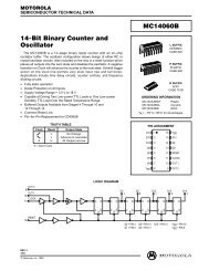
<strong>L292</strong><br />
SWITCH-MODE DRIVER FOR DC MOTORS<br />
DRIVING CAPABILITY : 2 A, 36 V, 30 KHz<br />
2 LOGIC CHIP ENABLE<br />
EXTERNAL LOOP GAIN ADJUSTEMENT<br />
SINGLE POWER SUPPLY (18 TO 36 V)<br />
INPUT SIGNAL SYMMETRIC TO GROUND<br />
THERMAL PROTECTION<br />
Multiwatt 15<br />
DESCRIPTION<br />
The <strong>L292</strong> is a monolithic LSI circuit in 15-lead<br />
Multiwatt ® package. It is intended for use, together<br />
with L290 and L291, as a complete 3-chip motor<br />
positioning system for applications such as carriage/daisy-wheel<br />
position control in type-writes.<br />
The L290/1/2 system can be directly controlled by<br />
a microprocessor.<br />
ORDER CODE : <strong>L292</strong><br />
ABSOLUTE MAXIMUM RATINGS<br />
Symbol Parameter Value Unit<br />
V s Power Supply 36 V<br />
V i Input Voltage - 15 to + Vs V<br />
Vinhibit Inhibit Voltage 0 to Vs V<br />
I o Output Current 2.5 A<br />
Ptot Total Power Dissipation (T case = 75 °C) 25 W<br />
T stg Storage and Junction Temperature - 40 to + 150 °C<br />
TRUTH TABLE<br />
CONNECTION DIAGRAM (top view)<br />
Vinhibit<br />
Pin 12 Pin 13<br />
Output Stage<br />
Condition<br />
L L Disabled<br />
L H Normal Operation<br />
H L Disabled<br />
H H Disabled<br />
March 1993<br />
1/12
<strong>L292</strong><br />
THERMAL DATA<br />
Symbol Parameter Value Unit<br />
Rth-j-case Thermal resistance junction-case Max 3 °C/W<br />
ELECTRICAL CHARACTERISTICS (V s = 36 V, T amb = 25 °C, f osc = 20 KHz unless otherwise specified)<br />
Symbol Parameter Test conditions Min. Typ. Max. Unit<br />
Vs Supply Voltage 18 36 V<br />
I d Quiescent Drain Current V s = 20 V (offset null) 30 50 mA<br />
V os Input Offset Voltage (pin 6) I o = 0 ±350 mV<br />
Vinh Inhibit Low Level (pin 12, 13) 2 V<br />
Inhibit High Level (pin 12, 13) 3.2 V<br />
I inh Low Voltage Condition V inh(L) = 0.4 V - 100 µA<br />
High Voltage Conditions V inh(H) = 3.2 V 10 µA<br />
Ii Input Current (pin 6) Vl = -8.8 V<br />
V l = +8.8 V<br />
V i Input Voltage (pin 6) R s1 = R s2 = 0.2Ω I o = 2A 9.1 V<br />
I o = -2A -9.1 V<br />
Io Output Current V l = ± 9.8 V R s1 = R s2 = 0.2 Ω ± 2 A<br />
V D Total Drop Out Voltage (inluding sensing I o = 2 A 5 V<br />
resistors)<br />
I o = 1 A 3.5 V<br />
V RS<br />
Sensing Rsistor Voltage<br />
Drop<br />
Tj = 150°C I o = 2 A 0.44 V<br />
I o Transconductance Rs1 = Rs2 =0.2Ω 205 220 235 mA/V<br />
V i<br />
Rs1 = Rs2 = 0.4Ω 120 mA/V<br />
f osc Frequency Range (pin 10) 1 30 KHz<br />
-1.8<br />
0.5<br />
mA<br />
mA<br />
BLOCK DIAGRAM AND TEST CIRCUIT<br />
2/12
<strong>L292</strong><br />
SYSTEM DESCRIPTION<br />
The L290, L291 and <strong>L292</strong> are intended to be used<br />
as a 3-chip microprocessor controlled positioning<br />
system. The device may be used separately - particularly<br />
the <strong>L292</strong> motor driver - but since they will<br />
usually be used together, a description of a typical<br />
L290/1/2 system follows.<br />
At the time, the microprocessor orders a switch to<br />
the position mode, (strobe signal at pin 8 of L291)<br />
and within 3 to 4 ms the <strong>L292</strong> drives the motor to<br />
a null position, where it is held by electronic "detenting".<br />
The mechanical/electrical interface consists of an<br />
Figure 1. System Block Diagram<br />
The system operates in two modes to achieve high<br />
speed, high-accurancy positioning.<br />
Speed commands for the system originate in the<br />
microprocessor. It is continuosly updated on the<br />
motor position by means of pulses from the L290<br />
tachometer chip, whitch in tur gets its information<br />
from the optical encoder. From this basic input, the<br />
microprocessor computes a 5-bit control word that<br />
sets the system speed dependent on the distance<br />
to travel.<br />
When the motor is stopped and the microprocessor<br />
orders it to a new positio, the system operates<br />
initially in an open-loop configuration as there is no<br />
feedback from the tachometer generator. A maximum<br />
speed is reached, the tachometer chip output<br />
backs off the processor signal thus reducing accelering<br />
torque. The motor continues to run at rop<br />
speed but under closed-loop control.<br />
As the target position is approached, the microprocessor<br />
lowers the value of the speed-demand word;<br />
this reduces the voltage at the main summing point,<br />
in effect braking the motor. The braking is applied<br />
progressively until the motor is running at minimum<br />
speed.<br />
optical encoder which generates two sinusoidal<br />
signals 90° out of phase (leading according to the<br />
motor direction) and proportional in frequency to the<br />
speed of rotation. The optical encoder also provides<br />
an output at one position on the disk which is used<br />
to set the initial position.<br />
The opto encoder signals, FTA and FTB are filtered<br />
by the networks R2C 2 and R 3 C 3 (referring to Fig.4)<br />
and are supplied to the FTA/FTB inputs on the L290.<br />
The main function on the L290 is to implement the<br />
following expression:<br />
Output signal (TACHO) = dVAB<br />
dt<br />
• FTA<br />
| FTA | − dVAA<br />
• FTB<br />
dt | FTB |<br />
Thus the mean value of TACHO is proportional to<br />
the rotation speed and its polarity indicates the<br />
direction of rotation.<br />
The above function is performed by amplifying the<br />
input signals in A 1 and A 2 to obtain V AA and V AB<br />
(typ.7 V p). From V AA and V AB the external differentiatior<br />
RC networks R 5 C 6 and R 4 C 4 give the signals<br />
V MA and V MB which are fed to the multipliers.<br />
3/12
<strong>L292</strong><br />
The second input to each multipler consists of the<br />
sign of the first input of the other multiplier before<br />
differentiation, these are obtained using the comparators<br />
C s1 and C s2. The multiplier outputs, C SA and<br />
C SB, are summed by A 3 to give the final output<br />
signal TACHO. The peak-topeak ripple signal of the<br />
TACHO can be found from the following expression:<br />
V ripple p − p = π 4 ( √ 2 − 1 ) • V thaco DC<br />
The max value of TACHO is:<br />
V tacho max = π 4<br />
√ 2 • V thaco DC<br />
Using the coparators C 1 and C 2 another two signals<br />
from V AA and V AB are derived - the logic signals STA<br />
and STB.<br />
This signals are used by the microprocessor to<br />
determine the position by counting the pulses.<br />
The L2910 internal reference voltage is also derived<br />
from V AA and V AB:<br />
V ref = | V AA | + | V AB |<br />
This reference is used by the D/A converter in the<br />
L291 to compensate for variations in input levels,<br />
temperature changes and ageing.<br />
The "one pulse per rotation" opto encoder output<br />
is connected to pin 12 of the L290 (FTF) where it is<br />
squared to give the STF logic output for the microprocessor.<br />
The TACHO signal and V ref are sent to the L291 via<br />
filter networks R 8 C 8 R 9 and R 6 C 7 R 7 respectively.<br />
Pin 12 of this chip is the main summing point of the<br />
system where TACHO and the D/A converter output<br />
are compared.<br />
The input to D/A converter consists of 5 bit word<br />
plus a sign bit supplied by the microprocessor. The<br />
sign bit represets the direction of motor rotation.<br />
The (analogue) output of the D/A conveter -<br />
DAC/OUT - is compared with the TACHO signal and<br />
the risulting error signal is amplified by the error<br />
amplifier, and subsequently appears on pin 1.<br />
The ERRV sognal (from pin 1 , L291) is fed to pin<br />
6 of the final chip, the <strong>L292</strong> H-bridge motor-driver.<br />
This input signals is bidirectional so it must be<br />
converted to a positive signal bacause the <strong>L292</strong><br />
uses a single supply voltage. This is accomplished<br />
by the first stage - the level shifter, which uses an<br />
internally generated 8 V reference.<br />
This same reference voltage supplies the triangle<br />
wave oscillator whose frequency is fixed by the<br />
external RC network (R20, C 17 - pins 11 and 10)<br />
where:<br />
1 f osc =<br />
1<br />
2RC<br />
(with R ≥ 8.2 K Ω)<br />
The oscillator determines the switching frequency<br />
of the output stage and should be in the range 1 to<br />
30 KHz.<br />
Motor current is regulated by an internal loop in the<br />
<strong>L292</strong> which is performed by the resistors R 18, R 19<br />
and the differential current sense amplifier, the output<br />
of which is filtered by an external RC network<br />
and fed back to the error amplifier.<br />
The choise of the external components in these RC<br />
network (pins 5, 7, 9) is determined by the motor<br />
type and the bandwidth requirements. The values<br />
shown in the diagram are for a 5Ω, 5 MH motor.<br />
(See <strong>L292</strong> Transfer Function Calculation in Application<br />
Information).<br />
The error signal obtained by the addition of the input<br />
and the current feedback signals (pin 7) is used to<br />
pulse width modulate the oscillator signal by means<br />
of the comparator. The pulse width modulated signal<br />
controls the duty cycle of the Hbridge to give an<br />
output current corresponding to the <strong>L292</strong> input<br />
signal.<br />
The interval between one side of the bridge switching<br />
off and the other switching on, τ, is programmed<br />
by C17 in conjuction with an internal resistor Rτ.<br />
This can be foud from:<br />
τ = Rτ • C pin 10. (C 17 in the diagram)<br />
Since Rτ is approximately 1.5 KΩ and the recommended<br />
τ to avoid simultaneous conduction is 2.5<br />
µs C pin 10 should be around 1.5 nF.<br />
The current sense resistors R 18 and R 19 should be<br />
high precision types (maximum tolerance ± 2 %)<br />
and the recommended value is given by:<br />
R max • I o max ≤ 0.44 V<br />
It is possible to synchronize two <strong>L292</strong> ’s, if desired,<br />
using the network shown in fig. 2.<br />
Finally, two enable inputs are provited on the <strong>L292</strong><br />
(pins 12 and 13-active low and high respectively).<br />
Thus the output stage may be inhibited by taking<br />
pin 12 high or by taking pin 13 low. The output will<br />
also be inhibited if the supply voltage falls below 18<br />
V.<br />
4/12
<strong>L292</strong><br />
The enable inputs were implemented in this way<br />
because they are intended to be driven directly by<br />
a microprocessor. Currently available microprocessors<br />
may generates spikes as high as 1.5 V during<br />
power-up. These inputs may be used for a variety<br />
of applications such as motor inhibit during reset of<br />
the logical system and power-on reset (see fig. 3).<br />
Figure 2. Figure 3.<br />
Figure 4 . Application Circuit.<br />
5/12
<strong>L292</strong><br />
APPLICATION INFORMATION<br />
This section has been added in order to help the designer for the best choise of the values of external<br />
components.<br />
Figure 5. <strong>L292</strong> Block Diagram.<br />
The schematic diagram used for the Laplace analysis of the system is shown in fig. 6.<br />
Figure 6.<br />
RS1 = RS2 = RS (sensing resistors)<br />
1<br />
= 2.5 • 10 -3 Ω (current sensing amplifier transconductance)<br />
R 4<br />
L M = Motor inductance, R M = Motor resistance, I M = Motor current<br />
G mo =<br />
IM<br />
| s = 0 (DC transfer function from the input of the comparator (VTH) to the motor<br />
current (I M)).<br />
6/12
<strong>L292</strong><br />
Neglecting the VCEsat of the bridge transistors and the VBE of the diodes:<br />
G mo =<br />
1<br />
R M<br />
2 Vs<br />
V<br />
where : V S = supply voltage (1)<br />
R<br />
V R = 8 V (reference voltage)<br />
DC TRANSFER FUNCTION<br />
In order to be sure that the current loop is stable the following condition is imposed :<br />
1 + sRC = 1 + s LM<br />
R M<br />
(pole cancellation) (2)<br />
from which RC = LM<br />
R M<br />
(Note that in practice R must greater than 5.6 KΩ)<br />
The transfer function is then,<br />
I M<br />
V I<br />
(s) =<br />
R 2 R 4<br />
R 1 R 3<br />
G mo<br />
1 + s R F C F<br />
G mo R s + s R 4 C + s 2 R F C F R 4 C<br />
(3)<br />
In DC condition, this is reduced to<br />
I M<br />
V I<br />
(o) =<br />
R 2 R 4<br />
R 1 R 3<br />
1<br />
• = 0.044 [ A R s R s V ] (4)<br />
OPEN-LOOP GAIN AND STABILITY CRITERION<br />
For RC = L M / R M, the open loop gain is:<br />
Aβ =<br />
1<br />
sR subF C • G mo R s<br />
R 4<br />
R F<br />
= G mo R s<br />
C<br />
1 + s R F C F R 4<br />
1<br />
s (1 + s R F C F )<br />
(5)<br />
In order to achieve good stability, the phase margin must be greater than 45° when | Aβ | = 1.<br />
1<br />
That means that, at f F =<br />
must be | Aβ | < 1 (see fig. 7), that is :<br />
2 π R F C F<br />
| A β | f =<br />
1<br />
2 π R F C F<br />
= G mo R s<br />
R 4 C<br />
R F C F<br />
√ 2 < 1 (6)<br />
Figure 7. Open Loop Frequency Response<br />
7/12
<strong>L292</strong><br />
CLOSED-LOOP SYSTEM STEP RESPONSE<br />
a) Small - signals analysis.<br />
Figure 8. Small Signal Step Response<br />
0.044<br />
t<br />
I M (t) = (1 − cos e − t<br />
2 R F C F ) Vi<br />
R s 2 R F C F<br />
The transfer function (3) can be written as follows:<br />
(normalized amplitude vs.<br />
t / R FC F).<br />
I M<br />
V I<br />
(s) =<br />
s<br />
1 +<br />
0.044 2 ξ ω o<br />
R s 2 ξs + s<br />
1 +<br />
ω o ω 2 o<br />
(7)<br />
√⎺⎺⎺⎺⎺⎺ Gmo R⎺<br />
s<br />
where wo =<br />
is the cutoff frequency<br />
R 4 C RF CF<br />
√⎺⎺⎺⎺⎺⎺⎺⎺⎺⎺⎺⎺ R 4 C<br />
ξ =<br />
4 R F C F G mo R s<br />
is the dumping factor<br />
By choosing the ξ value, it is possible to determine<br />
the system response to an input step signal.<br />
Examples :<br />
1) ξ = 1 from which<br />
V7 = 200 mV/div.<br />
I M = 100 mA/div.<br />
t = 100 µs/div.<br />
with V I = 1.5 Vp.<br />
I M (t) = 0.044 [ 1 − e − t<br />
2R F C F<br />
t (1 + ) ] • V i<br />
R s 4 R F C F<br />
(where Vi is the amplitude of the input step).<br />
1<br />
2) ξ = from which<br />
√ 2<br />
8/12
<strong>L292</strong><br />
It is possible to verify that the <strong>L292</strong> works in "closedloop"<br />
conditions during the entire motor current<br />
rise-time: the voltage at pin 7 inverting input of the<br />
error amplifier) is locked to the reference voltage<br />
V R, present at the non-inverting input of the same<br />
amplifier.<br />
The previous linear analysis is correct for this example.<br />
Descresing the ξ value, the rise-time of the current<br />
decreases. But for a good stability, from relationship<br />
(6), the maximum value of ξ is:<br />
CLOSED LOOP SYSTEM BANDWIDTH.<br />
A good choice for x is the value 1 / √2. In this case :<br />
I M<br />
V I<br />
(s) = 0.044<br />
R s<br />
The module of the transfer function is :<br />
| IM V I<br />
| = 0.044<br />
R s<br />
2<br />
ξmin =<br />
2 4 √⎺ 2<br />
1 + s R F C F<br />
1 + 2s R F C F + 2s 2 R 2 F C 2 F<br />
√⎺⎺⎺⎺⎺⎺⎺⎺⎺⎺⎺⎺⎺<br />
1 + ω 2 R 2 F C F 2<br />
0.9<br />
2π R F C F<br />
√⎺⎺⎺⎺⎺⎺⎺⎺⎺⎺⎺⎺⎺⎺⎺⎺⎺⎺⎺⎺⎺⎺⎺⎺⎺⎺⎺⎺⎺⎺⎺⎺⎺⎺⎺⎺⎺⎺⎺⎺⎺⎺<br />
[ ( 1 + 2 ω R F C F ) 2 + 1 ] • [ ( 1 − 2 ω R F C F ) 2 + 1 ]<br />
The cutoff frequency is derived by the expression (9) by putting | IM | = 0.707 • 0.044 (−3 dB), from<br />
V I R<br />
which :<br />
s<br />
ω T =<br />
0.9<br />
RF CF<br />
f T =<br />
1<br />
(phase margin = 45°)<br />
b) Large signal reponse<br />
The large step signal response is limited by slewrate<br />
and inductive load.<br />
In this case, during the rise-time of the motor<br />
current, The <strong>L292</strong> works is open-loop condition.<br />
(8)<br />
(9)<br />
9/12
<strong>L292</strong><br />
Example :<br />
a) Data - Motors characteristics: LM = 5 mH<br />
RM = 5 W<br />
L M / R M = 1msec<br />
- Voltage and current characteristics:<br />
V s = 20 V I M = 2 A V I = 9.1 V<br />
- Closed loop bandwidth : 3 kHz<br />
b) Calculation - From relationship (4) :<br />
R s =<br />
0.044<br />
I M<br />
V I = 0.2 Ω<br />
and from (1) :<br />
G mo =<br />
2VS<br />
R M V R<br />
= 1 Ω −1<br />
- RC = 1 msec [from expression (2) ].<br />
- Assuming ξ = 1/ √2 ; from (7) follows :<br />
ξ 2 = 1 2 =<br />
400 C<br />
4R F C F • 0.2<br />
- The cutoff frequency is :<br />
f T =<br />
143 • 10−3<br />
R F C F<br />
= 3 kHz<br />
c) Summarising<br />
- RC = 1.10 -3 sec<br />
- 1000 C = 1<br />
R F C F<br />
- R F C F ≅ 47 µs<br />
⎧<br />
⎨<br />
⎩<br />
C = 47 nF<br />
R = 22 KΩ<br />
For RF = 510 Ω → CF = 92 nF<br />
10/12
<strong>L292</strong><br />
MULTIWATT15 PACKAGE MECHANICAL DATA<br />
DIM.<br />
mm<br />
inch<br />
MIN. TYP. MAX. MIN. TYP. MAX.<br />
A 5 0.197<br />
B 2.65 0.104<br />
C 1.6 0.063<br />
D 1 0.039<br />
E 0.49 0.55 0.019 0.022<br />
F 0.66 0.75 0.026 0.030<br />
G 1.02 1.27 1.52 0.040 0.050 0.060<br />
G1 17.53 17.78 18.03 0.690 0.700 0.710<br />
H1 19.6 0.772<br />
H2 20.2 0.795<br />
L 21.9 22.2 22.5 0.862 0.874 0.886<br />
L1 21.7 22.1 22.5 0.854 0.870 0.886<br />
L2 17.65 18.1 0.695 0.713<br />
L3 17.25 17.5 17.75 0.679 0.689 0.699<br />
L4 10.3 10.7 10.9 0.406 0.421 0.429<br />
L7 2.65 2.9 0.104 0.114<br />
M 4.25 4.55 4.85 0.167 0.179 0.191<br />
M1 4.63 5.08 5.53 0.182 0.200 0.218<br />
S 1.9 2.6 0.075 0.102<br />
S1 1.9 2.6 0.075 0.102<br />
Dia1 3.65 3.85 0.144 0.152<br />
11/12
<strong>L292</strong><br />
Information furnished is believed to be accurate and reliable. However, SGS-THOMSON Microelectronics assumes no responsibility for the<br />
consequences of use of such information nor for any infringement of patents or other rights of third parties which may result from its use. No<br />
license is granted by implication or otherwise under any patent or patent rights of SGS-THOMSON Microelectronics. Specifications mentioned<br />
in this publication are subject to change without notice. This publication supersedes and replaces all information previously supplied.<br />
SGS-THOMSON Microelectronics products are not authorized for use as critical components in life support devices or systems without express<br />
written approval of SGS-THOMSON Microelectronics.<br />
© 1994 SGS-THOMSON Microelectronics - All Rights Reserved<br />
SGS-THOMSON Microelectronics GROUP OF COMPANIES<br />
Australia - Brazil - France - Germany - Hong Kong - Italy - Japan - Korea - Malaysia - Malta - Morocco - The Netherlands - Singapore -<br />
Spain - Sweden - Switzerland - <strong>Taiwan</strong> - Thaliand - United Kingdom - U.S.A.<br />
12/12