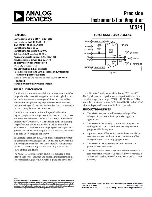
AD524 Precision Instrumentation Amplifier Data ... - Analog Devices
AD524 Precision Instrumentation Amplifier Data ... - Analog Devices
AD524 Precision Instrumentation Amplifier Data ... - Analog Devices

Create successful ePaper yourself
Turn your PDF publications into a flip-book with our unique Google optimized e-Paper software.
<strong>AD524</strong>TABLE OF CONTENTSFeatures .............................................................................................. 1Functional Block Diagram .............................................................. 1General Description ......................................................................... 1Product Highlights ........................................................................... 1Revision History ............................................................................... 2Specifications ..................................................................................... 3Absolute Maximum Ratings ............................................................ 8Connection Diagrams .................................................................. 8ESD Caution .................................................................................. 8Typical Performance Characteristics ............................................. 9Test Circuits ................................................................................. 14Theory of Operation ...................................................................... 15Input Protection .......................................................................... 15Input Offset and Output Offset ................................................ 15Gain .............................................................................................. 16Input Bias Currents .................................................................... 17Common-Mode Rejection ........................................................ 17Grounding ................................................................................... 18Sense Terminal ............................................................................ 18Reference Terminal .................................................................... 18Programmable Gain ................................................................... 20Autozero Circuits ....................................................................... 20Error Budget Analysis ................................................................ 21Outline Dimensions ....................................................................... 24Ordering Guide .......................................................................... 25REVISION HISTORY11/07—Rev. E to Rev. FUpdated Format .................................................................. UniversalChanges to General Description .................................................... 1Changes to Figure 1 .......................................................................... 1Changes to Figure 3 and Figure 4 Captions .................................. 8Changes to Error Budget Analysis Section ................................. 21Changes to Ordering Guide .......................................................... 254/99—Rev. D to Rev. ERev. F | Page 2 of 28
SPECIFICATIONS@ VS = ±15 V, RL = 2 kΩ and TA = +25°C, unless otherwise noted.<strong>AD524</strong>All min and max specifications are guaranteed. Specifications shown in boldface are tested on all production units at the final electricaltest. Results from those tests are used to calculate outgoing quality levels.Table 1.<strong>AD524</strong>A<strong>AD524</strong>BParameter Min Typ Max Min Typ Max UnitGAINGain Equation (External Resistor Gain Programming)⎡ 40,000 ⎤⎡ 40,000 ⎤⎢ + 1⎥± 20% ⎢ + 1⎥± 20%⎣ R G ⎦⎣ R G ⎦Gain Range (Pin Programmable) 1 to 1000 1 to 1000Gain Error 1G = 1 ±0.05 ±0.03 %G = 10 ±0.25 ±0.15 %G = 100 ±0.5 ±0.35 %G = 1000 ±2.0 ±1.0 %NonlinearityG = 1 ±0.01 ±0.005 %G = 10, G = 100 ±0.01 ±0.005 %G = 1000 ±0.01 ±0.01 %Gain vs. TemperatureG = 1 5 5 ppm/°CG = 10 15 10 ppm/°CG = 100 35 25 ppm/°CG = 1000 100 50 ppm/°CVOLTAGE OFFSET (May be Nulled)Input Offset Voltage 250 100 μVvs. Temperature 2 0.75 μV/°COutput Offset Voltage 5 3 mVvs. Temperature 100 50 μVOffset Referred to the Input vs. SupplyG = 1 70 75 dBG = 10 85 95 dBG = 100 95 105 dBG = 1000 100 110 dBINPUT CURRENTInput Bias Current ±50 ±25 nAvs. Temperature ±100 ±100 pA/°CInput Offset Current ±35 ±15 nAvs. Temperature ±100 ±100 pA/°CRev. F | Page 3 of 28
<strong>AD524</strong><strong>AD524</strong>A<strong>AD524</strong>BParameter Min Typ Max Min Typ Max UnitINPUTInput ImpedanceDifferential Resistance 10 9 10 9 ΩDifferential Capacitance 10 10 pFCommon-Mode Resistance 10 9 10 9 ΩCommon-Mode Capacitance 10 10 pFInput Voltage RangeMaximum Differential Input Linear (VDL) 2 ±10 ±10 VMaximum Common-Mode Linear (VCM) 2⎛ G ⎞⎛ G ⎞ V12 V − ⎜ × VD⎟ 12 V − ⎜ × VD⎟⎝ 2 ⎠ ⎝ 2 ⎠Common-Mode Rejection DC to 60 Hz with 1 kΩ Source ImbalanceVG = 1 70 75 dBG = 10 90 95 dBG = 100 100 105 dBG = 1000 110 115 dBOUTPUT RATINGVOUT, RL = 2 kΩ ±10 ±10 VDYNAMIC RESPONSESmall Signal – 3 dBG = 1 1 1 MHzG = 10 400 400 kHzG = 100 150 150 kHzG = 1000 25 25 kHzSlew Rate 5.0 5.0 V/μsSettling Time to 0.01%, 20 V StepG = 1 to 100 15 15 μsG = 1000 75 75 μsNOISEVoltage Noise, 1 kHzRTI 7 7 nV/√HzRTO 90 90 nV√HzRTI, 0.1 Hz to 10 HzG = 1 15 15 μV p-pG = 10 2 2 μV p-pG = 100, 1000 0.3 0.3 μV p-pCurrent Noise0.1 Hz to 10 Hz 60 60 pA p-pSENSE INPUTRIN 20 20 kΩ ± 20%IIN 15 15 μAVoltage Range ±10 ±10 VGain to Output 1 1 %REFERENCE INPUTRIN 40 40 kΩ ± 20%IIN 15 15 μAVoltage Range ±10 ±10 VGain to Output 1 1 %Rev. F | Page 4 of 28
<strong>AD524</strong><strong>AD524</strong>A<strong>AD524</strong>BParameter Min Typ Max Min Typ Max UnitTEMPERATURE RANGESpecified Performance –25 +85 –25 +85 °CStorage –65 +150 –65 +150 °CPOWER SUPPLYPower Supply Range ±6 ±15 ±18 ±6 ±15 ±18 VQuiescent Current 3.5 5.0 3.5 5.0 mA1Does not include effects of external resistor, RG.2VOL is the maximum differential input voltage at G = 1 for specified nonlinearity.VDL at the maximum = 10 V/G.VD = actual differential input voltage.Example: G = 10, VD = 0.50.VCM = 12 V − (10/2 × 0.50 V) = 9.5 V.@ VS = ±15 V, RL = 2 kΩ and TA = +25°C, unless otherwise noted.All min and max specifications are guaranteed. Specifications shown in boldface are tested on all production units at the final electricaltest. Results from those tests are used to calculate outgoing quality levels.Table 2.<strong>AD524</strong>C<strong>AD524</strong>SParameter Min Typ Max Min Typ Max UnitGAINGain Equation (External Resistor Gain Programming)⎡ 40,000 ⎤⎡ 40,000 ⎤⎢ + 1⎥± 20% ⎢ + 1⎥± 20%⎣ R G ⎦⎣ R G ⎦Gain Range (Pin Programmable) 1 to 1000 1 to 1000Gain Error 1G = 1 ±0.02 ±0.05 %G = 10 ±0.1 ±0.25 %G = 100 ±0.25 ±0.5 %G = 1000 ±0.5 ±2.0 %NonlinearityG = 1 ±0.003 ±0.01 %G = 10, G = 100 ±0.003 ±0.01 %G = 1000 ±0.01 ±0.01 %Gain vs. TemperatureG = 1 5 5 ppm/°CG = 10 10 10 ppm/°CG = 100 25 25 ppm/°CG = 1000 50 50 ppm/°CVOLTAGE OFFSET (May be Nulled)Input Offset Voltage 50 100 μVvs. Temperature 0.5 2.0 μV/°COutput Offset Voltage 2.0 3.0 mVvs. Temperature 25 50 μVOffset Referred to the Input vs. SupplyG = 1 80 75 dBG = 10 100 95 dBG = 100 110 105 dBG = 1000 115 110 dBRev. F | Page 5 of 28
<strong>AD524</strong><strong>AD524</strong>C<strong>AD524</strong>SParameter Min Typ Max Min Typ Max UnitINPUT CURRENTInput Bias Current ±15 ±50 nAvs. Temperature ±100 ±100 pA/°CInput Offset Current ±10 ±35 nAvs. Temperature ±100 ±100 pA/°CINPUTInput ImpedanceDifferential Resistance 10 9 10 9 ΩDifferential Capacitance 10 10 pFCommon-Mode Resistance 10 9 10 9 ΩCommon-Mode Capacitance 10 10 pFInput Voltage RangeMaximum Differential Input Linear (VDL) 2 ±10 ±10 VMaximum Common-Mode Linear (VCM) 2⎛ G ⎞⎛ G ⎞ V12 V − ⎜ × VD⎟ 12 V − ⎜ × VD⎟⎝ 2 ⎠ ⎝ 2 ⎠Common-Mode Rejection DC to 60 Hz with 1 kΩ Source ImbalanceVG = 1 80 70 dBG = 10 100 90 dBG = 100 110 100 dBG = 1000 120 110 dBOUTPUT RATINGVOUT, RL = 2 kΩ ±10 ±10 VDYNAMIC RESPONSESmall Signal – 3 dBG = 1 1 1 MHzG = 10 400 400 kHzG = 100 150 150 kHzG = 1000 25 25 kHzSlew Rate 5.0 5.0 V/μsSettling Time to 0.01%, 20 V StepG = 1 to 100 15 15 μsG = 1000 75 75 μsNOISEVoltage Noise, 1 kHzRTI 7 7 nV/√HzRTO 90 90 nV√HzRTI, 0.1 Hz to 10 HzG = 1 15 15 μV p-pG = 10 2 2 μV p-pG = 100, 1000 0.3 0.3 μV p-pCurrent Noise0.1 Hz to 10 Hz 60 60 pA p-pSENSE INPUTRIN 20 20 kΩ ± 20%IIN 15 15 μAVoltage Range ±10 ±10 VGain to Output 1 1 %Rev. F | Page 6 of 28
<strong>AD524</strong><strong>AD524</strong>C<strong>AD524</strong>SParameter Min Typ Max Min Typ Max UnitREFERENCE INPUTRIN 40 40 kΩ ± 20%IIN 15 15 μAVoltage Range 10 10 VGain to Output 1 1 %TEMPERATURE RANGESpecified Performance –25 +85 –55 +85 °CStorage –65 +150 –65 +150 °CPOWER SUPPLYPower Supply Range ±6 ±15 ±18 ±6 ±15 ±18 VQuiescent Current 3.5 5.0 3.5 5.0 mA1Does not include effects of external resistor RG.2VOL is the maximum differential input voltage at G = 1 for specified nonlinearity.VDL at the maximum = 10 V/G.VD = actual differential input voltage.Example: G = 10, VD = 0.50.VCM = 12 V − (10/2 × 0.50 V) = 9.5 V.Rev. F | Page 7 of 28
<strong>AD524</strong>ABSOLUTE MAXIMUM RATINGSTable 3.ParameterSupply VoltageInternal Power DissipationInput Voltage 1(Either Input Simultaneously) |VIN| + |VS|Output Short-Circuit DurationStorage Temperature Range(R)(D, E)Operating Temperature Range<strong>AD524</strong>A/<strong>AD524</strong>B/<strong>AD524</strong>C<strong>AD524</strong>SLead Temperature (Soldering, 60 sec)Rating±18 V450 mW
<strong>AD524</strong>TYPICAL PERFORMANCE CHARACTERISTICS208INPUT VOLTAGE (±V)15105+25°CQUIESCENT CURRENT (mA)64200 5 10 15 20SUPPLY VOLTAGE (±V)Figure 5. Input Voltage Range vs. Supply Voltage, G = 100500-00500 5 10 15 20SUPPLY VOLTAGE (±V)Figure 8. Quiescent Current vs. Supply Voltage00500-008201614OUTPUT VOLTAGE SWING (±V)15105INPUT BIAS CURRENT (±nA)121086400500-006200500-00900 5 10 15 2000 5 10 15 20SUPPLY VOLTAGE (±V)SUPPLY VOLTAGE (±V)Figure 6. Output Voltage Swing vs. Supply VoltageFigure 9. Input Bias Current vs. Supply Voltage304030OUTPUT VOLTAGE SWING (V p-p)2010INPUT BIAS CURRENT (nA)20100–10–20010 100 1k 10kLOAD RESISTANCE (Ω)00500-007–30–40–75 –25 25 75 125TEMPERATURE (°C)00500-010Figure 7. Output Voltage Swing vs. Load ResistanceFigure 10. Input Bias Current vs. TemperatureRev. F | Page 9 of 28
<strong>AD524</strong>1614–140–120G = 1000G = 100INPUT BIAS CURRENT (±nA)1210864CMRR (dB)–100–80–60–40G = 10G = 1200 5 10 15 20INPUT VOLTAGE (±V)Figure 11. Input Bias Current vs. Input Voltage00500-011–2000 10 100 1k 10k 100k 1M 10MFREQUENCY (Hz)Figure 14. CMRR vs. Frequency, RTI, Zero to 1000 Source Imbalance00500-014300ΔV OS FROM FINAL VALUE (µV)12345600500-012FULL POWER RESPONSE (V p-p)2010G = 1, 10, 100BANDWIDTH LIMITEDG = 1000 G = 100 G = 1000500-0150 1 2 3 4 5 6 7WARM-UP TIME (Minutes)Figure 12. Offset Voltage, RTI, Turn-On Drift801k 10k 100k 1MFREQUENCY (Hz)Figure 15. Large Signal Frequency Response1081000GAIN (V/V)100101SLEW RATE (V/µs)64G = 100020 10 100 1k 10k 100k 1M 10MFREQUENCY (Hz)Figure 13. Gain vs. Frequency00500-01301 10 100 1000GAIN (V/V)Figure 16. Slew Rate vs. Gain00500-016Rev. F | Page 10 of 28
<strong>AD524</strong>POWER SUPPLY REJECTION RATIO (dB)16014012010080604020010 100 1k 10k100kFREQUENCY (Hz)+V S = 15V DC +1V p-p SINEWAVEG = 1000G = 100G = 10G = 1Figure 17. Positive PSRR vs. Frequency00500-017CURRENT NOISE SPECTRAL DENSITY (fA/ Hz)100k10k1k1000 1 10 100 1k 10kFREQUENCY (Hz)Figure 20. Input Current Noise vs. Frequency00500-020POWER SUPPLY REJECTION RATIO (dB)16014012010080604020010 100 1k 10k100kFREQUENCY (Hz)G = 1000G = 100G = 10G = 1Figure 18. Negative PSRR vs. Frequency–V S = –15V DC +1V p-p SINEWAVE00500-0180.1Hz TO 10Hz5mV1sVERTICAL SCALE; 1 DIVISION = 5µVFigure 21. Low Frequency Noise, G = 1 (System Gain = 1000)00500-02110000.1Hz TO 10Hz100G = 110mV1sVOLT NSD (nV/ Hz)10G = 10G = 100, 1000G = 100010.11 10 100 1k 10k 100kFREQUENCY (Hz)Figure 19. RTI Noise Spectral Density vs. Gain00500-019VERTICAL SCALE; 1 DIVISION = 0.1µVFigure 22. Low Frequency Noise, G = 1000 (System Gain = 100,000)00500-022Rev. F | Page 11 of 28
<strong>AD524</strong>–12 TO +12–8 TO +8–4 TO +4OUTPUTSTEP (V)+4 TO –41% 0.1% 0.01%1mV 10V 10µs+8 TO –81% 0.1% 0.01%+12 TO –120 5 10 15 20SETTLING TIME (µs)Figure 23. Settling Time, Gain = 100500-023Figure 26. Large Signal Pulse Response and Settling Time, Gain = 1000500-0261mV10V 10µs–12 TO +12–8 TO +81%0.1%0.01%–4 TO +4OUTPUTSTEP (V)+4 TO –4Figure 24. Large Signal Pulse Response and Settling Time, Gain =100500-024+8 TO –81% 0.01%+12 TO –120.1%0 5 10 15 20SETTLING TIME (µs)Figure 27. Settling Time, Gain = 10000500-027–12 TO +12–8 TO +81%0.1%0.01%1mV 10V 10µs–4 TO +4OUTPUTSTEP (V)+4 TO –4+8 TO –81% 0.1% 0.01%+12 TO –120 5 10 15 20SETTLING TIME (µs)Figure 25. Settling Time, Gain = 1000500-025Figure 28. Large Signal Pulse Response and Settling Time, Gain = 10000500-028Rev. F | Page 12 of 28
<strong>AD524</strong>–12 TO +12–8 TO +8–4 TO +4OUTPUTSTEP (V)+4 TO –41% 0.1% 0.01%5mV 10V 20µs+8 TO –81% 0.1% 0.01%+12 TO –120 10 20 30 40 50 60 70 80SETTLING TIME (µs)Figure 29. Settling Time, Gain = 100000500-029Figure 30. Large Signal Pulse Response and Settling Time, Gain = 100000500-030Rev. F | Page 13 of 28
<strong>AD524</strong>TEST CIRCUITSINPUT20V p-p100kΩ0.1%11kΩ 1kΩ 100Ω0.1% 0.1% 0.1%10kΩ0.01% 1kΩ10T10kΩ0.1%+V S1 –RG 1816G = 101310G = 10012 <strong>AD524</strong>9G = 1000116RG 2372 +–V SFigure 31. Settling Time Test CircuitV OUT00500-031+V SI 150µAV BI 250µAA1 A2+C3+C4R5320kΩR5220kΩSENSE–INCH 2 ,CH 3 , CH 4CH 1I 350µAR5720kΩR56Q1, Q3 20kΩ Q2, Q44.44kΩRG 1 404ΩRG 2G = 10040ΩG = 1000I 450µAR5420kΩCH 2 , CH 3 ,CH 4A3R5520kΩCH 1V OREFERENCE+IN–V SFigure 32. Simplified Circuit of <strong>Amplifier</strong>; Gain Is Defined as((R56 + R57)/(RG)) +1; For a Gain of 1, RG Is an Open Circuit00500-032Rev. F | Page 14 of 28
<strong>AD524</strong>THEORY OF OPERATIONThe <strong>AD524</strong> is a monolithic instrumentation amplifier basedon the classic 3-op amp circuit. The advantage of monolithicconstruction is the closely matched components that enhancethe performance of the input preamplifier. The preamplifiersection develops the programmed gain by the use of feedbackconcepts. The programmed gain is developed by varying thevalue of RG (smaller values increase the gain) while the feedbackforces the collector currents (Q1, Q2, Q3, and Q4) to be constant,which impresses the input voltage across RG.As RG is reduced to increase the programmed gain, thetransconductance of the input preamplifier increases to thetransconductance of the input transistors. This has threeimportant advantages. First, this approach allows the circuitto achieve a very high open-loop gain of 3 × 10 8 at a programmedgain of 1000, thus reducing gain-related errors to a negligible30 ppm. Second, the gain bandwidth product, which is determinedby C3 or C4 and the input transconductance, reaches25 MHz. Third, the input voltage noise reduces to a valuedetermined by the collector current of the input transistorsfor an RTI noise of 7 nV/√Hz at G = 1000.INPUT PROTECTIONAs interface amplifiers for data acquisition systems, instrumentationamplifiers are often subjected to input overloads,that is, voltage levels in excess of the full scale for the selectedgain range. At low gains (10 or less), the gain resistor acts as acurrent limiting element in series with the inputs. At high gains,the lower value of RG does not adequately protect the inputsfrom excessive currents. Standard practice is to place serieslimiting resistors in each input, but to limit input current tobelow 5 mA with a full differential overload (36 V) requiresover 7kΩ of resistance, which adds 10 nV√Hz of noise. Toprovide both input protection and low noise, a special seriesprotection FET is used.A unique FET design was used to provide a bidirectionalcurrent limit, thereby protecting against both positive andnegative overloads. Under nonoverload conditions, threechannels (CH2, CH3, CH4) act as a resistance (≈1 kΩ) in serieswith the input as before. During an overload in the positivedirection, a fourth channel, CH1, acts as a small resistance(≈3 kΩ) in series with the gate, which draws only the leakagecurrent, and the FET limits IDSS. When the FET enhances undera negative overload, the gate current must go through the smallFET formed by CH1 and when this FET goes into saturation,the gate current is limited and the main FET goes into controlledenhancement. The bidirectional limiting holds the maximuminput current to 3 mA over the 36 V range.INPUT OFFSET AND OUTPUT OFFSETVoltage offset specifications are often considered a figure ofmerit for instrumentation amplifiers. While initial offset maybe adjusted to zero, shifts in offset voltage due to temperaturevariations causes errors. Intelligent systems can often correctthis factor with an autozero cycle, but there are many smallsignalhigh-gain applications that do not have this capability.+V S1 –816AD71210+V s131010016.2kΩ12 <strong>AD524</strong>93 + 8 1µF10001161/2 1 5 +RG 29.09kΩ 1/231µF2 –776 – 42 +1µFG = 1, 10, 100–V SG = 1000–V S1kΩ100Ω1.62MΩFigure 33. Noise Test Circuit16.2kΩ1.82kΩ00500-033Rev. F | Page 15 of 28
<strong>AD524</strong>Voltage offset and drift comprise two components each; inputand output offset and offset drift. Input offset is the componentof offset that is directly proportional to gain, that is, input offsetas measured at the output at G = 100 is 100 times greater than atG = 1. Output offset is independent of gain. At low gains, outputoffset drift is dominant, at high gains, input offset drift dominates.Therefore, the output offset voltage drift is normally specified asdrift at G = 1 (where input effects are insignificant), whereasinput offset voltage drift is given by drift specification at a highgain (where output offset effects are negligible). All inputrelated numbers are referred to the input (RTI) that is the effecton the output is G times larger. Voltage offset vs. power supplyis also specified at one or more gain settings and is also RTI.By separating these errors, one can evaluate the total errorindependent of the gain setting used. In a given gain configuration,both errors can be combined to give a total error referredto the input (RTI) or output (RTO) by the following formulas:Total error RTI = input error + (output error/gain)Total error RTO = (gain × input error) + output errorAs an illustration, a typical <strong>AD524</strong> might have a +250 μVoutput offset and a −50 μV input offset. In a unity gainconfiguration, the total output offset would be 200 μV orthe sum of the two. At a gain of 100, the output offset wouldbe −4.75 mV or: +250 μV + 100(−50 μV) = −4.75 mV.The <strong>AD524</strong> provides for both input and output offset adjustment.This simplifies very high precision applications and minimizesoffset voltage changes in switched gain applications. In suchapplications, the input offset is adjusted first at the highestprogrammed gain, then the output offset is adjusted at G = 1.GAINThe <strong>AD524</strong> has internal high accuracy pretrimmed resistorsfor pin programmable gains of 1, 10, 100, and 1000. One of thepreset gains can be selected by pin strapping the appropriategain terminal and RG2 together (for G = 1, RG2 is not connected).INPUTOFFSETNULL8–INPUT10kΩRG 2 374RG 1 16G = 10 13510G = 100 12 <strong>AD524</strong>96G = 100011+INPUT2Figure 34. Operating Connections for G = 100V OUTOUTPUTSIGNALCOMMON00500-034The <strong>AD524</strong> can be configured for gains other than those thatare internally preset; there are two methods to do this. The firstmethod uses just an external resistor connected betweenPin 3 and Pin 16 (see Figure 35), which programs the gainaccording to the following formula:R G40 kΩ= G = −1For best results, RG should be a precision resistor with a lowtemperature coefficient. An external RG affects both gainaccuracy and gain drift due to the mismatch between it andthe internal thin-film resistors. Gain accuracy is determinedby the tolerance of the external RG and the absolute accuracyof the internal resistors (±20%). Gain drift is determined by themismatch of the temperature coefficient of RG and the temperaturecoefficient of the internal resistors (−50 ppm/°C typical).–INPUT1.5kΩ1kΩ+INPUT1RG 1 16132.105kΩ1211RG 2 32+V S8<strong>AD524</strong>7–V S1069V OUTREFERENCE40,000G = + 1 = 20 ±20%2.105Figure 35. Operating Connections for G = 20The second method uses the internal resistors in parallel withan external resistor (see Figure 36). This technique minimizesthe gain adjustment range and reduces the effects of temperaturecoefficient sensitivity.–INPUT1RG 116G = 10 134kΩ1211RG 2 3+INPUT2*R| G = 10 = 4444.44Ω*R| G = 100 = 404.04Ω*R| G = 1000 = 40.04Ω*NOMINAL (±20%)+V S8<strong>AD524</strong>7–V S106V OUTREFERENCE40,000G =+ 1 = 20 ±17%4000||4444.44Figure 36. Operating Connections for G = 20, Low GainTemperature Coefficient Technique900500-03600500-035Rev. F | Page 16 of 28
<strong>AD524</strong>The <strong>AD524</strong> can also be configured to provide gain in the outputstage. Figure 37 shows an H pad attenuator connectedto the reference and sense lines of the <strong>AD524</strong>. R1, R2, and R3should be made as low as possible to minimize the gain variationand reduction of CMRR. Varying R2 precisely sets the gainwithout affecting CMRR. CMRR is determined by the matchof R1 and R3.–INPUT+INPUTG =1RG 1 16G = 10 13G = 100 12G = 1000 11RG 232(R2||40kΩ) + R1 + R3(R2||40kΩ)+V S8<strong>AD524</strong>71069R12.26kΩR25kΩR32.26kΩR L–V S(R1 + R2 + R3)||R L ≥ 2kΩFigure 37. Gain of 2000V OUTTable 4. Output Gain Resistor ValuesOutput Gain R2 R1, R3 Nominal Gain2 5 kΩ 2.26 kΩ 2.025 1.05 kΩ 2.05 kΩ 5.0110 1 kΩ 4.42 kΩ 10.1INPUT BIAS CURRENTSInput bias currents are those currents necessary to bias theinput transistors of a dc amplifier. Bias currents are anadditional source of input error and must be considered ina total error budget. The bias currents, when multiplied bythe source resistance, appear as an offset voltage. What is ofconcern in calculating bias current errors is the change in biascurrent with respect to signal voltage and temperature. Inputoffset current is the difference between the two input biascurrents. The effect of offset current is an input offset voltagewhose magnitude is the offset current times the sourceimpedance imbalance.23111213161+–+V S8<strong>AD524</strong>7–V S1069LOADTO POWERSUPPLYGROUNDFigure 38. Indirect Ground Returns for Bias Currents—Transformer Coupled00500-03800500-03723111213161+–+V S8<strong>AD524</strong>71069LOAD–V S TO POWERSUPPLYGROUNDFigure 40. Indirect Ground Returns for Bias Currents–AC-CoupledAlthough instrumentation amplifiers have differential inputs,there must be a return path for the bias currents. If this is notprovided, those currents charge stray capacitances, causing theoutput to drift uncontrollably or to saturate. Therefore, whenamplifying floating input sources such as transformers andthermocouples, as well as ac-coupled sources, there must stillbe a dc path from each input to ground.COMMON-MODE REJECTIONCommon-mode rejection is a measure of the change in outputvoltage when both inputs are changed equal amounts. Thesespecifications are usually given for a full-range input voltagechange and a specified source imbalance. Common-moderejection ratio (CMRR) is a ratio expression whereas commonmoderejection (CMR) is the logarithm of that ratio. Forexample, a CMRR of 10,000 corresponds to a CMR of 80 dB.In an instrumentation amplifier, ac common-mode rejection isonly as good as the differential phase shift. Degradation of accommon-mode rejection is caused by unequal drops acrossdiffering track resistances and a differential phase shift dueto varied stray capacitances or cable capacitances. In manyapplications, shielded cables are used to minimize noise. Thistechnique can create common-mode rejection errors unless theshield is properly driven. Figure 41 and Figure 42 show activedata guards that are configured to improve ac common-moderejection by bootstrapping the capacitances of the input cabling,thus minimizing differential phase shift.100ΩAD711+V S–INPUT1 –8G = 10012RG 2<strong>AD524</strong>3+INPUT2+–V S10Figure 41. Shield Driver, G ≥ 100769V OUT00500-040REFERENCE00500-04123111213161+–+V S8<strong>AD524</strong>71069LOAD–V STO POWERSUPPLYGROUNDFigure 39. Indirect Ground Returns for Bias Currents—Thermocouple00500-039100Ω100Ω+V S–INPUT1 –AD712 RG 18161012 <strong>AD524</strong>6–V S3RG 272 ++INPUT–V SFigure 42. Differential Shield Driver9V OUTREFERENCE00500-042Rev. F | Page 17 of 28
<strong>AD524</strong>GROUNDINGMany data acquisition components have two or more groundpins that are not connected together within the device. Thesegrounds must be tied together at one point, usually at the systempower-supply ground. Ideally, a single solid ground would bedesirable. However, because current flows through the groundwires and etch stripes of the circuit cards, and because thesepaths have resistance and inductance, hundreds of millivolts canbe generated between the system ground point and the dataacquisition components. Separate ground returns should beprovided to minimize the current flow in the path from thesensitive points to the system ground point. In this way, supplycurrents and logic-gate return currents are not summed into thesame return path as analog signals where they would causemeasurement errors.Because the output voltage is developed with respect to thepotential on the reference terminal, an instrumentationamplifier can solve many grounding problems.218<strong>AD524</strong>OUTPUTREFERENCE0.1µF670.1µF109ANALOG P.S.+15V C –15V0.1µFDIGCOMAD583SAMPLEAND HOLDANALOGGROUND*0.1µFDIGITAL P.S.+5VC1µF 1µFSIGNALGROUNDAD574A1µF7 9 11 15 1DIGITALDATAOUTPUT*IF INDEPENDENT; OTHERWISE, RETURN AMPLIFIER REFERENCETO MECCA AT ANALOG P.S. COMMON.Figure 43. Basic Grounding Practice00500-043SENSE TERMINALThe sense terminal is the feedback point for the instrumentamplifier’s output amplifier. Normally, it is connected to theinstrument amplifier output. If heavy load currents are to bedrawn through long leads, voltage drops due to current flowingthrough lead resistance can cause errors. The sense terminal canbe wired to the instrument amplifier at the load, thus puttingthe IxR drops inside the loop and virtually eliminating thiserror source.V IN +V IN –V+(SENSE)2 8OUTPUTCURRENTBOOSTER310<strong>AD524</strong> 9 X112617 (REF)V–Figure 44. <strong>AD524</strong> <strong>Instrumentation</strong> <strong>Amplifier</strong> with Output Current BoosterTypically, IC instrumentation amplifiers are rated for a full±10 volt output swing into 2 kΩ. In some applications, however,the need exists to drive more current into heavier loads.Figure 44 shows how a high current booster may be connectedinside the loop of an instrumentation amplifier to provide therequired current boost without significantly degrading overallperformance. Nonlinearities and offset and gain inaccuracies ofthe buffer are minimized by the loop gain of the <strong>AD524</strong> outputamplifier. Offset drift of the buffer is similarly reduced.REFERENCE TERMINALThe reference terminal can be used to offset the output by up to±10 V. This is useful when the load is floating or does not sharea ground with the rest of the system. It also provides a directmeans of injecting a precise offset. It must be remembered thatthe total output swing is ±10 V to be shared between signal andreference offset.When the <strong>AD524</strong> is of the 3-amplifier configuration itis necessary that nearly zero impedance be presented to thereference terminal.Any significant resistance from the reference terminal toground increases the gain of the noninverting signal path,thereby upsetting the common-mode rejection of the <strong>AD524</strong>.In the <strong>AD524</strong>, a reference source resistance unbalances the CMRtrim by the ratio of 20 kΩ/RREF. For example, if the referencesource impedance is 1 Ω, CMR is reduced to 86 dB (20 kΩ/1 Ω= 86 dB). An operational amplifier can be used to provide thatlow impedance reference point, as shown in Figure 45. Theinput offset voltage characteristics of that amplifier adds directlyto the output offset voltage performance of the instrumentationamplifier.R L00500-044Rev. F | Page 18 of 28
<strong>AD524</strong>V IN +V IN –+V S2 83121<strong>AD524</strong>7–V S10SENSE96REFAD711LOADV OFFSETFigure 45. Use of Reference Terminal to Provide Output OffsetAn instrumentation amplifier can be turned into a voltageto-currentconverter by taking advantage of the sense andreference terminals, as shown in Figure 46.00500-045+INPUT–INPUT23131+–<strong>AD524</strong>SENSE10REFAD711V X V IN 40,000I L = = = (1 + )R1 R1 R G69A2R1V XLOADFigure 46. Voltage-to-Current ConverterBy establishing a reference at the low side of a current settingresistor, an output current may be defined as a function of inputvoltage, gain, and the value of that resistor. Because only a smallcurrent is demanded at the input of the buffer amplifier (A2)the forced current, IL, largely flows through the load. Offset anddrift specifications of A2 must be added to the output offset anddrift specifications of the <strong>AD524</strong>.I L00500-046–IN+ININPUTOFFSETTRIMR110kΩ123456PROTECTIONPROTECTION15R2+V S 10kΩ1420kΩ20kΩ20kΩ20kΩ20kΩ4.44kΩ13404Ω1240Ω1611OUTPUTOFFSETTRIMNCRELAYSHIELDSG = 10K1G = 100K2G = 1000K3–V S78A1<strong>AD524</strong>20kΩ109OUTK1 D1 K2 D2 K3 D3+5VANALOGCOMMON1µF35V+V SK1 – K3 =C1C2GAIN TABLEA B GAIN001101011010001001THERMOSEN DM2C4.5V COILD1 – D3 = IN4148INPUTS AGAINRANGE B+5V1 1623456774LS138DECODERNC = NO CONNECTFigure 47. Three-Decade Gain Programmable <strong>Amplifier</strong>151413Y0Y1Y21 162345677407NBUFFERDRIVER10µFLOGICCOMMON00500-047Rev. F | Page 19 of 28
<strong>AD524</strong>PROGRAMMABLE GAINFigure 47 shows the <strong>AD524</strong> being used as a software programmablegain amplifier. Gain switching can be accomplished withmechanical switches such as DIP switches or reed relays. It shouldbe noted that the on resistance of the switch in series with theinternal gain resistor becomes part of the gain equation and hasan effect on gain accuracy.The <strong>AD524</strong> can also be connected for gain in the output stage.Figure 48 shows an AD711 used as an active attenuator in theoutput amplifier’s feedback loop. The active attenuation presentsvery low impedance to the feedback resistors, thereforeminimizing the common-mode rejection ratio degradation.–IN+IN–V S+V S1µF35V(+INPUT)(–INPUT)INPUTOFFSETNULL123410kΩ5678PROTECTION16OUTPUTOFFSETPROTECTION15 NULL+V TO –VS14 R210kΩ4.44kΩ1320kΩ20kΩ20kΩ+ –<strong>AD524</strong>20kΩ20kΩ20kΩ20kΩAD7590404Ω1240Ω10pFV SS V DD GND+V S1 8 16–152+1314AD7111112–V SV DD93 4 5 6 7A2 A3 A4 WRFigure 48. Programmable Output Gain111091039.2kΩ28.7kΩ316kΩV OUT1kΩ1kΩ1kΩ00500-048+INPUT(–INPUT)1G = 10 13G = 100 12G = 1000 11RG 1 16RG 2–INPUT(+INPUT)32DATAINPUTSCSWRDAC A/DAC BPROTECTION4.44kΩ404Ω40ΩPROTECTION414 DB071516618DB7V b20kΩ+V S17 3DAC ADAC B20kΩAD75285<strong>AD524</strong>20kΩ20kΩ21192020kΩ20kΩ10961/2AD712256:11/2AD712Figure 49. Programmable Output Gain Using a DACAnother method for developing the switching scheme is touse a DAC. The AD7528 dual DAC, which acts essentially asa pair of switched resistive attenuators having high analoglinearity and symmetrical bipolar transmission, is ideal in thisapplication. The multiplying DAC’s advantage is that it canhandle inputs of either polarity or zero without affecting theprogrammed gain. The circuit shown uses an AD7528 to setthe gain (DAC A) and to perform a fine adjustment (DAC B).V OUTAUTOZERO CIRCUITSIn many applications, it is necessary to provide very accuratedata in high gain configurations. At room temperature, theoffset effects can be nulled by the use of offset trim potentiometers.Over the operating temperature range, however,offset nulling becomes a problem. The circuit of Figure 50shows a CMOS DAC operating in bipolar mode and connectedto the reference terminal to provide software controllable offsetadjustments.00500-049Rev. F | Page 20 of 28
<strong>AD524</strong>++V+INPUT2RG 1 168–V SRG 23–INPUT1 –7G = 10 1310G = 100 12 <strong>AD524</strong>9G = 1000 11639kΩVREF–V SR3AD589 +V S 20kΩ R520kΩMSB15 14 16 C1S41/2DATAOUT1R4INPUTS LSB12 – 8 10kΩ AD71211 AD752416 –OUT2CS 1223 +7WR 131/25 + 4AD712 R635kΩ–V SGND+V SFigure 50. Software Controllable OffsetIn many applications, complex software algorithms for autozeroapplications are not available. For those applications, Figure 51provides a hardware solution.15 1614132RG 1 16131211RG 231+–+V S810V OUT<strong>AD524</strong>99 106 0.1µF LOWCHLEAKAGE71kΩ–V –S12 11+AD71100500-050350Ω350Ω+10V350Ω350Ω+810kΩ24RG 23RG 1 16513G = 10012 <strong>AD524</strong>C111 – 7+V S–V SFigure 52. Typical Bridge Application106914-BITADC0V TO 2VF.S.ERROR BUDGET ANALYSISTo illustrate how instrumentation amplifier specifications areapplied, review a typical case where an <strong>AD524</strong> is required toamplify the output of an unbalanced transducer. Figure 52shows a differential transducer, unbalanced by 100 Ω, supplyinga 0 mV to 20 mV signal to an <strong>AD524</strong>C. The output of the IAfeeds a 14-bit ADC with a 0 V to 2 V input voltage range. Theoperating temperature range is −25°C to +85°C. Therefore, thelargest change in temperature, ΔT, within the operating range isfrom ambient to +85°C (85°C − 25°C = 60°C).In many applications, differential linearity and resolution are ofprime importance in cases where the absolute value of a variable isless important than changes in value. In these applications, onlythe irreducible errors (45 ppm = 0.004%) are significant. Furthermore,if a system has an intelligent processor monitoring theanalog-to-digital output, the addition of an autogain/autozerocycle removes all reducible errors and may eliminate the requirementfor initial calibration. This also reduces errors to 0.004%.00500-052V DD 8V SS 1GND 2200µsZERO PULSEA1 A2 A3 A4Figure 51. Autozero CircuitAD7510KD00500-051Rev. F | Page 21 of 28
<strong>AD524</strong>Table 5. Error Budget AnalysisError Source<strong>AD524</strong>CSpecificationsCalculationEffect onAbsoluteAccuracyat TA = 25°CEffect onAbsoluteAccuracyat TA = 85°CEffectonResolutionGain Error ±0.25% ±0.25% = 2500 ppm 2500 ppm 2500 ppm –Gain Instability 25 ppm (25 ppm/°C)(60°C) = 1500 ppm – 1500 ppm –Gain Nonlinearity ±0.003% ±0.003% = 30 ppm – – 30 ppmInput Offset Voltage ±50 μV, RTI ±50 μV/20 mV = ±2500 ppm 2500 ppm 2500 ppm –Input Offset Voltage Drift±0.5 μV/°C–(±0.5 μV/°C)(60°C) = 30 μV30 μV/20 mV = 1500 ppm– 1500 ppm –Output Offset Voltage 1 ±2.0 mV ±2.0 mV/20 mV = 1000 ppm 1000 ppm 1000 ppm –Output Offset Voltage Drift 1 ±25 μV/°C (±25 μV/°C)(60°C)= 1500 μV– 750 ppm –1500 μV/20 mV = 750 ppmBias Current-SourceImbalance Error±15 nA (±15 nA)(100 Ω ) = 1.5 μV1.5 μV/20 mV = 75 ppm75 ppm 75 ppm –Bias Current-SourceImbalance DriftOffset Current-SourceImbalance ErrorOffset Current-SourceImbalance DriftOffset Current-SourceResistance-ErrorOffset Current-SourceResistance-Drift±100 pA/°C (±100 pA/°C)(100 Ω )(60°C) = 0.6 μV0.6 μV/20 mV = 30 ppm±10 nA (±10 nA)(100 Ω ) = 1 μV1 μV/20 mV = 50 ppm±100 pA/°C (100 pA/°C)(100 Ω )(60°C) = 0.6 μV0.6 μV/20 mV = 30 ppm±10 nA (10 nA)(175 Ω ) = 3.5 μV3.5 μV/20 mV = 87.5 ppm±100 pA/°C (100 pA/°C)(175 Ω )(60°C) = 1 μV1 μV/20 mV = 50 ppm– 30 ppm –50 ppm 50 ppm –– 30 ppm –87.5 ppm 87.5 ppm –– 50 ppm –Common Mode Rejection 5 V DC 115 dB 115 dB = 1.8 ppm × 5 V = 8.8 μV 444 ppm 444 ppm –8.8 μV/20 mV = 444 ppmNoise, RTI (0.1 Hz to 10 Hz) 0.3 μV p-p 0.3 μV p-p/20 mV = 15 ppm – – 15 ppmTotal Error 6656.5 ppm 10516.5 ppm 45 ppm1Output offset voltage and output offset voltage drift are given as RTI figures.Rev. F | Page 22 of 28
<strong>AD524</strong>Figure 53 shows a simple application in which the variationof the cold-junction voltage of a Type J thermocouple-iron ±constantan is compensated for by a voltage developed in seriesby the temperature-sensitive output current of an AD590semiconductor temperature sensor.TYPEJKETS, RR ANOMINALVALUE52.3Ω41.2Ω61.4Ω40.2Ω5.76ΩMEASURINGJUNCTIONREFERENCEJUNCTION+15°C < T A < +35°CV AIRONV T CONSTANTANTA+V SI AAD5902.5V7.5VR ACU 52.3ΩE O = V T – V A + 52.3ΩI A + 2.5V– 2.5V1 + 52.3ΩR~ = V TR TAD580G = 100+V S<strong>AD524</strong>+E O–8.66kΩ1kΩNOMINAL VALUE9135ΩFigure 53. Cold-Junction Compensation–V SOUTPUTAMPLIFIEROR METERThe circuit is calibrated by adjusting RT for proper outputvoltage with the measuring junction at a known referencetemperature and the circuit near 25°C. If resistors with lowtemperature coefficients are used, compensation accuracy isto within ±0.5°C, for temperatures between +15°C and +35°C.00500-053Other thermocouple types may be accommodated with thestandard resistance values shown in Table 5. For other rangesof ambient temperature, the equation in Figure 53 may besolved for the optimum values of RT and RA.The microprocessor controlled data acquisition system shownin Figure 54 includes both autozero and autogain capability. Bydedicating two of the differential inputs, one to ground and oneto the A/D reference, the proper program calibration cycles caneliminate both initial accuracy errors and accuracy errors overtemperature. The autozero cycle, in this application, converts anumber that appears to be ground and then writes that samenumber (8-bit) to the AD7524, which eliminates the zero error.Because its output has an inverted scale, the autogain cycleconverts the A/D reference and compares it with full scale. Amultiplicative correction factor is then computed and appliedto subsequent readings.For a comprehensive study of instrumentation amplifierdesign and applications, refer to the Designer’s Guide to<strong>Instrumentation</strong> <strong>Amplifier</strong>s (3 rd Edition), available free from<strong>Analog</strong> <strong>Devices</strong>, Inc.AD7507A0, A2,EN, A12RG 216131211RG 1 3120kΩ+<strong>AD524</strong>–106AD5839AGND–V REF20kΩAD574ALATCH–+1/2AD71210kΩ –+1/25kΩ AD712AD7524DECODEV INV REFMICRO-CONTROLPROCESSORADDRESS BUSFigure 54. Microprocessor Controlled <strong>Data</strong> Acquisition System00500-054Rev. F | Page 23 of 28
<strong>AD524</strong>OUTLINE DIMENSIONS0.005 (0.13) MIN0.080 (2.03) MAXPIN 10.200 (5.08)MAX0.200 (5.08)0.125 (3.18)160.023 (0.58)0.014 (0.36)91 80.840 (21.34) MAX0.310 (7.87)0.220 (5.59)0.060 (1.52)0.015 (0.38)0.150(3.81)MIN0.100 0.070 (1.78) SEATING(2.54)PLANE0.030 (0.76)BSC0.320 (8.13)0.290 (7.37)0.015 (0.38)0.008 (0.20)CONTROLLING DIMENSIONS ARE IN INCHES; MILLIMETER DIMENSIONS(IN PARENTHESES) ARE ROUNDED-OFF INCH EQUIVALENTS FORREFERENCE ONLY AND ARE NOT APPROPRIATE FOR USE IN DESIGN.Figure 55. 16-Lead Side-Brazed Ceramic Dual In-Line [SBDIP](D-16)Dimensions shown in inches and (millimeters)0.358 (9.09)0.342 (8.69)SQ0.100 (2.54)0.064 (1.63)0.358(9.09)MAXSQ0.088 (2.24)0.054 (1.37)0.075 (1.91)REF0.095 (2.41)0.075 (1.90)0.011 (0.28)0.007 (0.18)R TYP0.075 (1.91)REF0.055 (1.40)0.045 (1.14)19318 20 41BOTTOMVIEW14130.200 (5.08)REF0.100 (2.54) REF890.150 (3.81)BSC0.015 (0.38)MIN0.028 (0.71)0.022 (0.56)0.050 (1.27)BSC45° TYPCONTROLLING DIMENSIONS ARE IN INCHES; MILLIMETER DIMENSIONS(IN PARENTHESES) ARE ROUNDED-OFF INCH EQUIVALENTS FORREFERENCE ONLY AND ARE NOT APPROPRIATE FOR USE IN DESIGN.Figure 56. 20-Terminal Ceramic Leadless Chip Carrier [LCC](E-20)Dimensions shown in inches and (millimeters)022106-A10.50 (0.4134)10.10 (0.3976)16 97.60 (0.2992)7.40 (0.2913)1810.65 (0.4193)10.00 (0.3937)0.30 (0.0118)0.10 (0.0039)COPLANARITY1.27 (0.0500)BSC2.65 (0.1043)2.35 (0.0925)0.10 0.51 (0.0201) SEATINGPLANE 0.33 (0.0130)0.31 (0.0122)0.20 (0.0079)8°0°0.75 (0.0295)0.25 (0.0098)45°1.27 (0.0500)0.40 (0.0157)COMPLIANT TO JEDEC STANDARDS MS-013- AACONTROLLING DIMENSIONS ARE IN MILLIMETERS; INCH DIMENSIONS(IN PARENTHESES) ARE ROUNDED-OFF MILLIMETER EQUIVALENTS FORREFERENCE ONLY AND ARE NOT APPROPRIATE FOR USE IN DESIGN.Figure 57. 16-Lead Standard Small Outline Package [SOIC_W]Wide Body (RW-16)Dimensions shown in millimeters and (inches)032707-BRev. F | Page 24 of 28
<strong>AD524</strong>ORDERING GUIDEModel Temperature Range Package Description Package Option<strong>AD524</strong>AD −40°C to +85°C 16-Lead SBDIP D-16<strong>AD524</strong>ADZ 1 −40°C to +85°C 16-Lead SBDIP D-16<strong>AD524</strong>AE −40°C to +85°C 20-Terminal LCC E-20<strong>AD524</strong>AR-16 −40°C to +85°C 16-Lead SOIC_W RW-16<strong>AD524</strong>AR-16-REEL −40°C to +85°C 16-Lead SOIC_W, 13" Tape and Reel RW-16<strong>AD524</strong>AR-16-REEL7 −40°C to +85°C 16-Lead SOIC_W, 7" Tape and Reel RW-16<strong>AD524</strong>ARZ-16 1 −40°C to +85°C 16-Lead SOIC_W RW-16<strong>AD524</strong>ARZ-16-REEL7 1 −40°C to +85°C 16-Lead SOIC_W, 7”Tape and Reel RW-16<strong>AD524</strong>BD −40°C to +85°C 16-Lead SBDIP D-16<strong>AD524</strong>BDZ 1 −40°C to +85°C 16-Lead SBDIP D-16<strong>AD524</strong>BE −40°C to +85°C 20-Terminal LCC E-20<strong>AD524</strong>CD −40°C to +85°C 16-Lead SBDIP D-16<strong>AD524</strong>CDZ 1 −40°C to +85°C 16-Lead SBDIP D-16<strong>AD524</strong>SD −55°C to +125°C 16-Lead SBDIP D-16<strong>AD524</strong>SD/883B −55°C to +125°C 16-Lead SBDIP D-165962-8853901EA 2 −55°C to +125°C 16-Lead SBDIP D-16<strong>AD524</strong>SE/883B −55°C to +125°C 20-Terminal LCC E-20<strong>AD524</strong>SCHIPS −55°C to +125°C Die1Z = RoHS Compliant Part.2Refer to the official DESC drawing for tested specifications.Rev. F | Page 25 of 28
<strong>AD524</strong>NOTESRev. F | Page 26 of 28
<strong>AD524</strong>NOTESRev. F | Page 27 of 28
<strong>AD524</strong>NOTES©2007 <strong>Analog</strong> <strong>Devices</strong>, Inc. All rights reserved. Trademarks andregistered trademarks are the property of their respective owners.D00500-0-11/07(F)Rev. F | Page 28 of 28