CD4027BM CD4027BC Dual JK Master Slave Flip-Flop with Set and ...
CD4027BM CD4027BC Dual JK Master Slave Flip-Flop with Set and ...
CD4027BM CD4027BC Dual JK Master Slave Flip-Flop with Set and ...

You also want an ePaper? Increase the reach of your titles
YUMPU automatically turns print PDFs into web optimized ePapers that Google loves.
<strong>CD4027BM</strong><strong>CD4027BC</strong> <strong>Dual</strong> J-K <strong>Master</strong><strong>Slave</strong><br />
<strong>Flip</strong>-<strong>Flop</strong> <strong>with</strong> <strong>Set</strong> <strong>and</strong> Reset<br />
General Description<br />
These dual J-K flip-flops are monolithic complementary<br />
MOS (CMOS) integrated circuits constructed <strong>with</strong> N- <strong>and</strong> P-<br />
channel enhancement mode transistors Each flip-flop has<br />
independent J K set reset <strong>and</strong> clock inputs <strong>and</strong> buffered<br />
Q <strong>and</strong> Q outputs These flip-flops are edge sensitive to the<br />
clock input <strong>and</strong> change state on the positive-going transition<br />
of the clock pulses <strong>Set</strong> or reset is independent of the clock<br />
<strong>and</strong> is accomplished by a high level on the respective input<br />
All inputs are protected against damage due to static discharge<br />
by diode clamps to V DD <strong>and</strong> V SS <br />
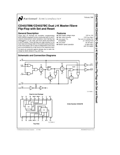
Schematic <strong>and</strong> Connection Diagrams<br />
<strong>Dual</strong>-In-Line Package<br />
Features<br />
February 1988<br />
Y Wide supply voltage range 30V to 15V<br />
Y High noise immunity 045 VDD (typ)<br />
Y Low power TTL Fan out of 2 driving 74L<br />
compatibility<br />
or 1 driving 74LS<br />
Y Low power 50 nW (typ)<br />
Y Medium speed operation 12 MHz (typ)<br />
<strong>with</strong> 10V supply<br />
Order Number CD4027B<br />
TLF5958–1<br />
<strong>CD4027BM</strong><strong>CD4027BC</strong> <strong>Dual</strong> J-K <strong>Master</strong><strong>Slave</strong> <strong>Flip</strong>-<strong>Flop</strong> <strong>with</strong> <strong>Set</strong> <strong>and</strong> Reset<br />
Top View<br />
TLF5958–2<br />
C1995 National Semiconductor Corporation<br />
TLF5958<br />
RRD-B30M105Printed in U S A
Absolute Maximum Ratings (Note 1 <strong>and</strong> 2)<br />
If MilitaryAerospace specified devices are required<br />
please contact the National Semiconductor Sales<br />
OfficeDistributors for availability <strong>and</strong> specifications<br />
DC Supply Voltage (V DD )<br />
b05 V DC to a18 V DC<br />
Input Voltage (V IN )<br />
b05V to V DD a05 V DC<br />
Storage Temperature Range (T S ) b65Ctoa150C<br />
Power Dissipation (P D )<br />
<strong>Dual</strong>-In-Line<br />
700 mW<br />
Small Outline<br />
500 mW<br />
Lead Temperature (T L )<br />
(Soldering 10 seconds)<br />
260C<br />
Recommended Operating<br />
Conditions (Note 2)<br />
DC Supply Voltage (V DD )<br />
Input Voltage (V IN )<br />
Operating Temperature Range (T A )<br />
<strong>CD4027BM</strong><br />
<strong>CD4027BC</strong><br />
3Vto15V DC<br />
0VtoV DD V DC<br />
b55Ctoa125C<br />
b40Ctoa85C<br />
DC Electrical Characteristics <strong>CD4027BM</strong> (Note 2)<br />
Symbol Parameter Conditions<br />
b55C a25C a125C<br />
Min Max Min Typ Max Min Max<br />
I DD Quiescent Device Current V DD e 5V V IN e V DD or V SS 1 1 30 mA<br />
V DD e 10V V IN e V DD or V SS 2 2 60 mA<br />
V DD e 15V V IN e V DD or V SS 4 4 120 mA<br />
V OL Low Level lI Ol k 1 mA<br />
Output Voltage V DD e 5V 005 0 005 005 V<br />
V DD e 10V 005 0 005 005 V<br />
V DD e 15V 005 0 005 005 V<br />
V OH High Level lI Ol k 1 mA<br />
Output Voltage V DD e 5V 495 495 5 495 V<br />
V DD e 10V 995 995 10 995 V<br />
V DD e 15V 1495 1495 15 1495 V<br />
V IL Low Level V DD e 5V V O e 05V or 45V 15 15 15 V<br />
Input Voltage V DD e 10V V O e 1V or 9V 30 30 30 V<br />
V DD e 15V V O e 15V or 135V 40 40 40 V<br />
V IH High Level V DD e 5V V O e 05V or 45V 35 35 35 V<br />
Input Voltage V DD e 10V V O e 1V or 9V 70 70 70 V<br />
V DD e 15V V O e 15V or 135V 110 110 110 V<br />
I OL Low Level Output V DD e 5V V O e 04V 064 051 088 036 mA<br />
Current (Note 3) V DD e 10V V O e 05V 16 13 225 09 mA<br />
V DD e 15V V O e 15V 42 34 88 24 mA<br />
I OH High Level Output V DD e 5V V O e 46V b064 b051 b088 b036 mA<br />
Current (Note 3) V DD e 10V V O e 95V b16 b13 b225 b09 mA<br />
V DD e 15V V O e 135V b42 b34 b88 b24 mA<br />
I IN Input Current V DD e 15V V IN e 0V b01 b10b5 b01 b10 mA<br />
V DD e 15V V IN e 15V 01 10 b5 01 10 mA<br />
Note 1 ‘‘Absolute Maximum Ratings’’ are those values beyond which the safety of the device cannot be guaranteed They are not meant to imply that the devices<br />
should be operated at these limits The table of ‘‘Recommended Operating Conditions’’ <strong>and</strong> ‘‘Electrical Characteristics’’ provides conditions for actual device<br />
operation<br />
Note 2 V SS e 0V unless otherwise specified<br />
Note 3 I OH <strong>and</strong> I OL are tested one output at a time<br />
Units<br />
2
DC Electrical Characteristics <strong>CD4027BC</strong> (Note 2)<br />
Symbol Parameter Conditions<br />
b40C a25C a85C<br />
Min Max Min Typ Max Min Max<br />
I DD Quiescent Device Current V DD e 5V V IN e V DD or V SS 4 4 30 mA<br />
V DD e 10V V IN e V DD or V SS 8 8 60 mA<br />
V DD e 15V V IN e V DD or V SS 16 16 120 mA<br />
V OL Low Level lI Ol k 1 mA<br />
Output Voltage V DD e 5V 005 0 005 005 V<br />
V DD e 10V 005 0 005 005 V<br />
V DD e 15V 005 0 005 005 V<br />
V OH High Level lI Ol k 1 mA<br />
Output Voltage V DD e 5V 495 495 5 495 V<br />
V DD e 10V 995 995 10 995 V<br />
V DD e 15V 1495 1495 15 1495 V<br />
V IL Low Level V DD e 5V V O e 05V or 45V 15 15 15 V<br />
Input Voltage V DD e 10V V O e 1V or 9V 30 30 30 V<br />
V DD e 15V V O e 15V or 135V 40 40 40 V<br />
V IH High Level V DD e 5V V O e 05V or 45V 35 35 35 V<br />
Input Voltage V DD e 10V V O e 1V or 9V 70 70 70 V<br />
V DD e 15V V O e 15V or 135V 110 110 110 V<br />
I OL Low Level Output V DD e 5V V O e 04V 052 044 088 036 mA<br />
Current (Note 3) V DD e 10V V O e 05V 13 11 225 09 mA<br />
V DD e 15V V O e 15V 36 30 88 24 mA<br />
I OH High Level Output V DD e 5V V O e 46V b052 b044 b088 b036 mA<br />
Current (Note 3) V DD e 10V V O e 95V b13 b11 b225 b09 mA<br />
V DD e 15V V O e 135V b36 b30 b88 b24 mA<br />
I IN Input Current V DD e 15V V IN e 0V b03 b10b5 b03 b10 mA<br />
V DD e 15V V IN e 15V 03 10 b5 03 10 mA<br />
Note 1 ‘‘Absolute Maximum Ratings’’ are those values beyond which the safety of the device cannot be guaranteed They are not meant to imply that the devices<br />
should be operated at these limits The table of ‘‘Recommended Operating Conditions’’ <strong>and</strong> ‘‘Electrical Characteristics’’ provides conditions for actual device<br />
operation<br />
Note 2 V SS e 0V unless otherwise specified<br />
Note 3 I OH <strong>and</strong> I OL are tested one output at a time<br />
Units<br />
3
AC Electrical Characteristics T A e 25C C L e 50 pF t rCL e t fCL e 20 ns unless otherwise specified<br />
Symbol Parameter Conditions Min Typ Max Units<br />
t PHL or t PLH Propagation Delay Time V DD e 5V 200 400 ns<br />
from Clock to Q or Q V DD e 10V 80 160 ns<br />
V DD e 15V 65 130 ns<br />
t PHL or t PLH Propagation Delay Time V DD e 5V 170 340 ns<br />
from <strong>Set</strong> to Q or Reset to Q V DD e 10V 70 140 ns<br />
V DD e 15V 55 110 ns<br />
t PHL or t PLH Propagation Delay Time V DD e 5V 110 220 ns<br />
from <strong>Set</strong> to Q or V DD e 10V 50 100 ns<br />
Reset to Q V DD e 15V 40 80 ns<br />
t S Minimum Data <strong>Set</strong>up Time V DD e 5V 135 270 ns<br />
V DD e 10V 55 110 ns<br />
V DD e 15V 45 90 ns<br />
t THL or t TLH Transition Time V DD e 5V 100 200 ns<br />
V DD e 10V 50 100 ns<br />
V DD e 15V 40 80 ns<br />
f CL Maximum Clock Frequency V DD e 5V 25 5 MHz<br />
(Toggle Mode) V DD e 10V 62 125 MHz<br />
V DD e 15V 76 155 MHz<br />
t rCL or t fCL Maximum Clock Rise V DD e 5V 15 ms<br />
<strong>and</strong> Fall Time V DD e 10V 10 ms<br />
V DD e 15V 5 ms<br />
t W Minimum Clock Pulse V DD e 5V 100 200 ns<br />
Width (t WH e t WL ) V DD e 10V 40 80 ns<br />
V DD e 15V 32 65 ns<br />
t WH Minimum <strong>Set</strong> <strong>and</strong> V DD e 5V 80 160 ns<br />
Reset Pulse Width V DD e 10V 30 60 ns<br />
V DD e 15V 25 50 ns<br />
C IN Average Input Capacitance Any Input 5 75 pF<br />
C PD Power Dissipation Capacity Per <strong>Flip</strong>-<strong>Flop</strong><br />
(Note 4)<br />
35 pF<br />
AC Parameters are guaranteed by DC correlated testing<br />
Note 1 ‘‘Absolute Maximum Ratings’’ are those values beyond which the safety of the device cannot be guaranteed They are not meant to imply that the<br />
devices should be operated at these limits The table of ‘‘Recommended Operating Conditions’’ <strong>and</strong> ‘‘Electrical Characteristics’’ provides conditions for actual<br />
device operation<br />
Note 2 V SS e 0V unless otherwise specified<br />
Note 3 I OH <strong>and</strong> I OL are tested one output at a time<br />
Note 4 C PD determines the no load AC power consumption of any CMOS device For complete explanation see 54C74C Family Characteristics application<br />
note AN-90<br />
4
Typical Applications<br />
Ripple Binary Counters<br />
TLF5958–3<br />
Shift Registers<br />
TLF5958–4<br />
Truth Table<br />
tnb1 Inputs<br />
X tn Outputs<br />
Where<br />
CLU J K S R Q Q Q<br />
L I X O O O I O<br />
L X O O O I I O<br />
L O X O O O O I<br />
L X I O O I O I<br />
K X X O O X (No Change)<br />
X X X I O X I O<br />
X X X O I X O I<br />
X X X I I X I I<br />
I e High Level<br />
O e Low Level<br />
U e Level Change<br />
X e Don’t Care<br />
e t nb1 refers to the time interval prior to the positive clock pulse transition<br />
X e t n refers to the time intervals after the positive clock pulse transition<br />
5
<strong>CD4027BM</strong><strong>CD4027BC</strong> <strong>Dual</strong> J-K <strong>Master</strong><strong>Slave</strong> <strong>Flip</strong>-<strong>Flop</strong> <strong>with</strong> <strong>Set</strong> <strong>and</strong> Reset<br />
Physical Dimensions inches (millimeters)<br />
LIFE SUPPORT POLICY<br />
Ceramic <strong>Dual</strong>-In-Line Package (J)<br />
Order Number <strong>CD4027BM</strong>J or <strong>CD4027BC</strong>J<br />
NS Package Number J16A<br />
Molded <strong>Dual</strong>-In-Line Package (N)<br />
Order Number <strong>CD4027BM</strong>N or <strong>CD4027BC</strong>N<br />
NS Package Number N16E<br />
NATIONAL’S PRODUCTS ARE NOT AUTHORIZED FOR USE AS CRITICAL COMPONENTS IN LIFE SUPPORT<br />
DEVICES OR SYSTEMS WITHOUT THE EXPRESS WRITTEN APPROVAL OF THE PRESIDENT OF NATIONAL<br />
SEMICONDUCTOR CORPORATION As used herein<br />
1 Life support devices or systems are devices or 2 A critical component is any component of a life<br />
systems which (a) are intended for surgical implant support device or system whose failure to perform can<br />
into the body or (b) support or sustain life <strong>and</strong> whose be reasonably expected to cause the failure of the life<br />
failure to perform when properly used in accordance support device or system or to affect its safety or<br />
<strong>with</strong> instructions for use provided in the labeling can effectiveness<br />
be reasonably expected to result in a significant injury<br />
to the user<br />
National Semiconductor National Semiconductor National Semiconductor National Semiconductor<br />
Corporation Europe Hong Kong Ltd Japan Ltd<br />
1111 West Bardin Road Fax (a49) 0-180-530 85 86 13th Floor Straight Block Tel 81-043-299-2309<br />
Arlington TX 76017 Email cnjwge tevm2nsccom Ocean Centre 5 Canton Rd Fax 81-043-299-2408<br />
Tel 1(800) 272-9959 Deutsch Tel (a49) 0-180-530 85 85 Tsimshatsui Kowloon<br />
Fax 1(800) 737-7018 English Tel (a49) 0-180-532 78 32 Hong Kong<br />
Franais Tel (a49) 0-180-532 93 58 Tel (852) 2737-1600<br />
Italiano Tel (a49) 0-180-534 16 80 Fax (852) 2736-9960<br />
National does not assume any responsibility for use of any circuitry described no circuit patent licenses are implied <strong>and</strong> National reserves the right at any time <strong>with</strong>out notice to change said circuitry <strong>and</strong> specifications
This datasheet has been downloaded from:<br />
www.DatasheetCatalog.com<br />
Datasheets for electronic components.